Controllers: How Five Consoles Read a Button
A controller has one job that is harder than it looks: get a dozen independent button states from the player’s hands into the CPU, over a cable thin enough to be comfortable, cheaply enough that two of them ship in the box. Twelve buttons cannot each have a wire. So every console in this era picked a way to squeeze them down to a handful of conductors, and the four different answers on this page are the reason a dead NES pad costs you fifty cents and a dead SNES pad costs you a whole donor controller.
I have the NES, Famicom, SNES, Genesis, N64 and GameCube documented separately, each with its own pin tables. This page is the cross-section: one axis, six machines, and what the answer predicts before you have the shell open.
The problem all of them are solving
Take twelve buttons at 5 V logic. The obvious approach (one wire per button) needs fourteen conductors with power and ground, and a cable that thick is miserable to hold and expensive to make. Every console here instead puts silicon inside the pad and sends the button states over serially, in time rather than in parallel. What differs is what that silicon is, and that turns out to be the whole story for repair.
Two families of answer show up:
- Shift register. Load all the buttons into a register in parallel on a strobe, then clock them out one bit at a time down a single data line. The NES and SNES both work this way.
- Multiplexer. Put two buttons on each data line and let the console pick which half it is looking at by toggling a select line. No storage, no clock. This is the Genesis.
Then by the N64 the pad stopped being logic at all and became a small computer that answers questions.
NES: an off-the-shelf part, and that is the point
The NES-004 pad is the most repairable controller of its generation, and the reason is one part number. Its shift register is a CD4021B, an ordinary 8-bit parallel-in / serial-out CMOS jellybean, sixteen pins, in production continuously since the 1970s and buyable today from any distributor for pocket change.
Eight buttons sit on eight parallel inputs and shift out of Q8. The inputs are held high by a 45 kΩ × 8 resistor network and pulled to ground by the carbon contact pads, so a button reading permanently pressed points at a contact or a pull-up before it points at the chip. Five conductors do the work: ground, +5 V, the latch strobe, the clock, and the data coming back.
The console side carries two extra data lines beyond that, which is how the Zapper, the Power Pad and the Arkanoid controller get their own path back without a different port.
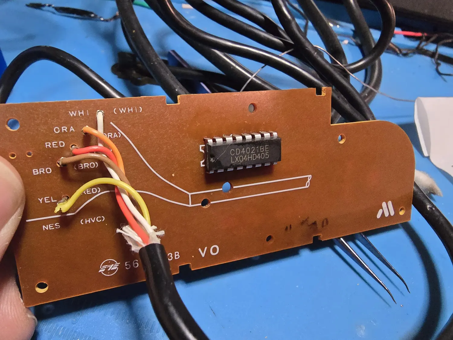
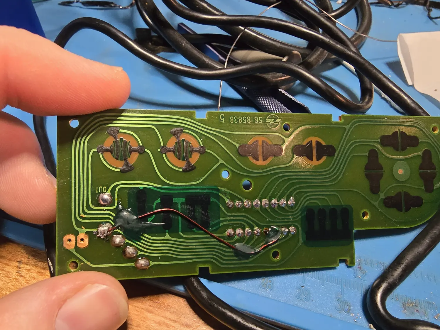
One detail catches people mid-repair: some pads fit a 3.6 kΩ resistor on the OUT0 latch line and some do not. The OEM drawing annotates it “not present in all models”, so its absence is not a fault to correct.
Pin tables for the CD4021 and the in-shell header are on the NES reference. The port numbering there is tagged single-source and I mean it: the signal set is not in doubt, but GameSX and NESdev disagree on the physical ordering, and I have not metered a port myself yet.
The Famicom keeps the chip and throws away the port
Same CD4021 inside, completely different repair. An original HVC-001 Famicom has no controller ports at all: both pads are hardwired, running back through the shell to a 5-conductor header for pad 1 and a 6-conductor header for pad 2. So the failure that on an NES means “swap the pad” is, on a Famicom, opening the console.
The two harnesses are not interchangeable, and this is where a rushed repair goes wrong: the pin order differs, and the wire colours differ. Red is ground on the pad-2 harness and nowhere else in the family. Trust the header legend, never the colour.
Pad 2’s extra conductor is a microphone, read as a single bit at $4016 bit 2 and also bled into the console’s audio mix, amplified by a 4069UB inverter inside the pad. It costs pad 2 its Select and Start buttons, which are physically absent and always read as not-pressed. The AV Famicom drops the mic entirely and moves to detachable 7-pin ports.
SNES: fourteen bits Nintendo would not sell you
The SNES pad is the same idea as the NES pad executed with parts nobody else can supply, and that single decision is why these are the pads I hoard donors for.
Nintendo built it two ways, and both are house silicon:
- Single-IC pads use one 56V520, a 14-bit parallel-in / serial-out shift register in a 20-pin package. Twelve inputs go to the carbon pads; two are spare.
- Dual-IC pads use two 56W545 8-bit shift registers cascaded: IC-B’s serial output feeds IC-A’s data input, and IC-A drives the console.
There is no logic-family substitute for either. A 4021 is 8-bit, and nothing common gives you fourteen stages in one package. A dead SNES shift register is a donor controller, not a parts order. Which variant you have is invisible from outside the shell.
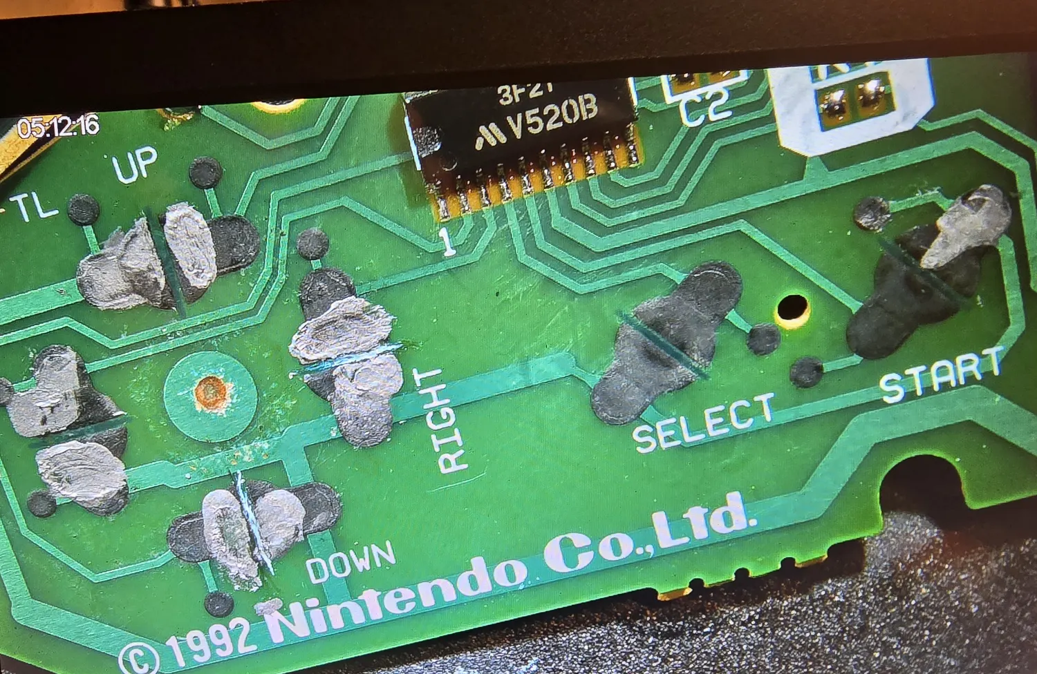
The dual-IC map shows the protocol directly. Data shifts toward Q8, so the highest-numbered input leaves first. IC-A carries Right, Left, Down, Up, Start, Select, Y, B on PI 1 through PI 8; IC-B carries R, L, X, A on PI 5 through PI 8. Shift from PI 8 downward and you get B, Y, Select, Start, Up, Down, Left, Right, A, X, L, R, which is exactly the twelve-bit order the software expects.
The port keeps the NES’s trick of extra lines for peripherals. Data2 is unused by a standard pad and carries splitters and multitaps. IOBit runs to the console’s I/O port at $4201/$4213, and on port 2 that bit is tied to the PPU counter latch, so anything plugged into port 2 can latch the H and V counters by pulling its IOBit low. The two published tables disagree here, and both are right from their own end: ConsoleMods lists pins 5 and 6 as no-connect because a standard pad has no wires on them, while the superfamicom wiki names them from the console side. The console-side names are the ones you want on a bench.
The pad has no regulator. VDD and VSS come straight from the console, so everything inside swings 0 to 5 V. A healthy console measures roughly 4.75 to 5.1 V at the pad; meaningfully lower is the console’s regulator talking, not the controller. Interfacing one to a 3.3 V microcontroller means level-shifting the data line coming back.
Genesis: no shift register at all
Sega solved the same problem with no storage and no clock. A 3-button pad is a 74HC157 quad 2-to-1 multiplexer (DIP on early boards, SOIC on later ones, and another genuine jellybean) steered by the SELECT (TH) line that the console drives on pin 7 of the DE-9.
The console sets TH, reads the port, flips TH, reads again. Each data pin therefore carries two different buttons depending on the state of TH: pin 6 is B or A, pin 9 is C or Start, and pins 3 and 4 report Left and Right with TH high but sit pulled to ground with TH low. Everything idles high on pull-ups until a game starts polling.
Two consequences follow on the bench.
Repairs are cheap. A 74HC157 costs pennies and the pull-ups are ordinary 10 kΩ resistors. Nothing in a 3-button pad is unobtainable.
Cable faults lie to you. Some lines are actively driven through the mux and others run passively to the cable. A short between the two classes lets a driven line overpower a passive one and report a direction nobody is pressing, which looks exactly like a stuck D-pad contact and is not.
6-button pads add their own controller IC, and what it does is watch the timing. It detects rapid SELECT toggling (under 12 ms between edges) and on the third low pulse returns all four directions low as an ID handshake, then exposes X, Y, Z and Mode on the next high. A pad that has to recognise a handshake needs real silicon, so 6-button pads land back in donor territory. That handshake is also why a handful of games misbehave with one, and why those pads have a Mode button at all: hold it at power-on and the pad presents itself as a 3-button.
That SELECT line has a second use with nothing to do with controllers. It is game-driven, so scoping pin 7 tells you whether a game is actually running. It idles high through the SEGA logo and starts pulsing once the game takes over: Sonic pulses low roughly every 20 ms, Mortal Kombat II does the inverse. Pulses with a black screen means the CPU and cartridge are fine and the fault is in the video chain. It is the fastest split I know between a video fault and a dead CPU.
N64 and GameCube: the pad becomes a computer
By 1996 the pad stopped being logic. The N64 controller port has three pins: 3.3 V, ground, and one bidirectional open-drain data line. There is no clock and no latch, because there is nothing to clock. The console’s PIF-NUS polls the pad over the Joybus protocol and the pad’s own NUS-CNT controller chip answers.
That buys a lot. The same three wires carry the analog stick, the rumble pak, the memory card and the Transfer Pak, because they are all just different answers to a query. The accessory port inside the pad is a plain 8-bit SRAM-style bus (sixteen address lines, eight data lines, the usual enables) which is precisely why a Controller Pak is a battery-backed SRAM cartridge.
It also means the repair story inverts. Nothing in an N64 pad is a jellybean, so the chip is donor-only. But the part that actually wears out is not the chip: it is the analog stick, and Nintendo made that a self-contained module on a 6-pin lead. Every replacement on the market (hall-effect, TMR, optical rebuild) drops into that same connector without a soldering iron. The stick is a pair of optical quadrature encoders reporting relative movement that the controller chip integrates into an absolute position, which is why a worn stick that is not centred at power-on stays wrong until it is re-centred.
The GameCube continues the idea on a 7-pin port: one bidirectional data line riding the SI block inside Flipper, a 3.43 V logic supply, and a separate 5 V rail purely for the rumble motor. Both rails leave through one shared front-panel PPTC fuse, which produces the diagnosis worth knowing on that machine: all four ports dead at once, console otherwise fine, is the fuse before it is Flipper. One port dead is not.
At a glance
| NES / Famicom | SNES | Genesis 3-button | Genesis 6-button | N64 | |
|---|---|---|---|---|---|
| Silicon in the pad | CD4021B | 56V520, or 2× 56W545 | 74HC157 | custom controller IC | NUS-CNT |
| Method | 8-bit shift register | 14 bits of shift register | 2-to-1 multiplex | multiplex + protocol | serial bus |
| Console drives | latch + clock | latch + clock | SELECT (TH) only | TH, extra cycles | polled queries |
| Data lines back | 1 (+2 for peripherals) | 1 (+Data2, IOBit) | 4, doubled by TH | 4, doubled by TH | 1, bidirectional |
| Port | 7-pin | 7-pin | DE-9 | DE-9 | 3-pin |
| Logic level | 5 V | 5 V | 5 V | 5 V | 3.3 V |
| Dead chip means | order a part | find a donor | order a part | find a donor | find a donor |
What this predicts before you open anything
Sort the same six machines by whether the silicon is obtainable and you get a clean split that has nothing to do with age or manufacturer:
Fixable from a parts order. NES, Famicom, Genesis 3-button. The active part is a jellybean still in production. Add a cable, a resistor network and some contact cleaner and there is no failure in these pads you cannot repair indefinitely.
Donor-only. SNES, Genesis 6-button, N64, GameCube. The active part was made for exactly one product and never sold across the counter. Everything around the chip is still fixable (cables, contacts, membranes, and on the N64 the stick module), but a failed controller IC ends the pad.
That is why my donor pile is shaped the way it is. Broken-shell SNES and 6-button Genesis pads with live boards are worth keeping; a broken-shell NES pad is worth keeping only for the cable and the plug.
The fault that is almost never the chip
Across all six machines, the controller ICs themselves are reliable. They sit in a warm dry shell doing almost nothing. Nearly everything that presents as a dead or erratic pad is one of three things, and they are the same three regardless of architecture.
The cable, at the strain relief. This is the overwhelming majority. Repeated flexing at the point where the cable enters the shell breaks a conductor inside intact-looking insulation. Every pad here lands its cable on an internal header or a row of solder pads, and that is where a replacement cable goes. Check this before suspecting anything electronic. On a Genesis pad, note which revision you have: the later boards use a white crimped connector block instead of direct-soldered wires, and I solder fresh wires to the underside of the block’s pins rather than fighting the block.
The carbon contact pads. The black pucks under the rubber membrane wear through, and a button that needs a hard press or reports intermittently is almost always this. Clean first, with isopropyl only. Never use an abrasive and never use a fibreglass pen: both strip the carbon permanently and turn a dirty pad into a worn one. Where replacement pad sets or silicone membranes exist, they are the tidier fix.
Conductive paint, as a last resort. When a pad has genuinely worn through, it works. Keep it thin and off the surrounding traces; a blob that bridges to a neighbour creates a stuck input, which on a Genesis pad is indistinguishable at first from the driven-versus-passive cable short described above.
Where the pin tables live
Each machine’s controller ICs, ports and internal headers are tabled on its own reference page, with the confidence tag on every entry:
- NES front-loader: CD4021, the 5-way internal header, the 7-pin port
- Famicom family: both hardwired harnesses, the pad-2 mic circuit, the AV Famicom’s 7-pin port
- SNES: 56V520, 56W545, the in-shell cable connector, the 7-pin port
- Genesis / Mega Drive: the DE-9 port with the full TH multiplex
- N64: the 3-pin port, the 32-pin accessory bus, PIF-NUS
- GameCube: the 7-pin port and its two fused rails