Sega Genesis / Mega Drive Repair Reference
The Sega Genesis, sold as the Mega Drive outside North America, is one of the more satisfying 16-bit machines to work on, because most of what fails on it is understood and fixable, and because the platform rewards knowing exactly which board is in front of you before you touch anything. That last part is the whole game here. Sega re-laid this board out roughly once a year for a decade, almost always to fold more discrete logic into a custom gate array, and those revisions change the audio circuit, the video encoder, the mod paths, and even the number of voltage regulators. A fix that is right for one revision is wrong or impossible on another. So this page leads with board identification and comes back to it constantly.
This is a reference for the standalone consoles: Model 1 revisions VA0 through VA7, and Model 2 revisions VA0 through VA2.3, NTSC and PAL. The Model 2 short boards (VA3, VA4 with its all-in-one GOAC die) and the Genesis 3 show up for lineage and the occasional bench visit, but they are not my core range and I flag them as context when they appear. The Sega CD and the 32X are separate devices with their own repair story, and they get their own page later. They intrude here in exactly one place that matters: the power connector, because the 32X shares the Model 2 supply and polarity, which is the opposite of the Model 1, while the Sega CD add-ons, confusingly, take the Model 1 type instead. More on that below, because it is the single most damaging mistake you can make on this platform.
Where the source material is thin or the community disagrees, I say so rather than papering over it. A few specific numbers on this platform rest on a single source, and I have called those out in plain language instead of pretending they are settled.
Know your board first
Because a bare Genesis PCB swaps between shells trivially, the case only narrows it down. The board confirms it. Here is the shape of the two families and then the per-revision detail.
The line splits into two case families with materially different A/V, audio, and power hardware:
| Model 1 (Genesis / Mega Drive) | Model 2 (Genesis II / Mega Drive II) | |
|---|---|---|
| Shape | Rectangular, ring around the cart port | Square, centered cart port |
| A/V out | Full-size 8-pin DIN (shared with the Master System) | 9-pin mini-DIN |
| Stereo audio | Front headphone jack only; the DIN carries mono | Stereo on the 9-pin port; no headphone jack |
| DC input | ~9 V NA / ~10 V PAL, center NEGATIVE, 5.5 x 2.1 mm barrel | ~10 V, center POSITIVE, EIAJ-03 4.75 x 1.7 mm |
| EXT port | Present VA0 through VA6 and all JP models; gone from VA6.5 on | None (expansion port for Sega CD only) |
Model 1 revisions (VA0 through VA7)
Revisions are silkscreened VAn on the board, with a few exceptions: “VA0” was never marked and is a retro-name, and “VA6.5” and “VA6.8” come from Sega service docs (VA6.8 is marked “V6.8”). The trend across the whole line is consolidation of discrete logic into Sega gate arrays.
- VA0 (837-6656, 1988, Japan only). Uses an EDCLK-fix daughterboard plus discrete 74LS00 glue. Overdriven preamp, the worst rainbow banding of any revision.
- VA1 (837-6832, 1989, Japan). The daughterboard and 74LS00 fold into the 315-5339 gate array.
- VA2 (837-6955 JP / 837-6992 NA, 1989, first North American board). 315-5339 becomes 315-5345, fixing a DMA-refresh glitch. The NA layout adds an internal RF modulator.
- VA3 (837-7071, 1989 to 1991, NA and first Brazil). The bus arbiter and clock generator merge into the 315-5364. Sega fixes the overdriven preamp and adds a gentle low-pass filter. This is the audio baseline enthusiasts prize. Some 1991 boards get the die-shrunk 315-5313A VDP.
- VA4 (837-7138 JP/KR / 171-5872-20 Asia/PAL, first Asia/PAL/Korea). Roughly a VA3 with the video encoder flipped and the circuit rearranged. Most PAL “High Definition Graphics, Stereo Sound” units are VA4.
- VA5 (171-5963, 1990 to 1991, Japan). The I/O and arbiter merge into the big 315-5402 gate array. Carries factory JP5/6/7 jumper wires, which are not a mod. Some 315-5402 boards show TMSS only in export mode.
- VA6 (171-5963-xx, 1991 to 1993, most regions). Same as VA5 but the I/O chip is the 315-5433, which brings the first TMSS (the “Produced by or under license” license screen). Last revision with the EXT port in most markets.
- VA6.5 (171-5963-10/-30, 1992 to 1993). A VA6 with the EXT port and line filters deleted, leaving a blank rear panel. Many use the 315-5313A VDP. The most common PAL Model 1.
- VA6.8 (171-5963-40, 1993, PAL only). Like VA6.5 but an SMD Fujitsu MB3514 encoder replaces the DIP Sony CXA1145P. Community documentation (ConsoleMods) reports that the factory omitted C30 on this board, so there is no mono audio in stock form and you get sound only from the headphone jack. I have not been able to corroborate the C30 detail against a second independent source, so treat it as a lead to verify on the board rather than a settled fact. Final PAL Model 1, and often confused with VA6.5.
- VA7 (171-6217-xx, 1992 to 1993, NA/JP/Brazil/Taiwan). A total redesign. The first standalone unit built on the Yamaha FC1004 ASIC (315-5487), which puts the VDP, the I/O, and a modified YM3438 FM core on one die. Single 7805 instead of two, SMD RAM, SMD CXA1145 encoder, PLCC 68000. On non-Japanese units the rear ports shift toward center, which is the fastest visual tell. The 315-5487 has a broken 50 Hz mode; some Brazilian VA7s use the fixed 315-5660.
A couple of oddities: VA7 is essentially a Genesis 2 board in a Genesis 1 case, and it even shares the PC PCB prefix. A Korean Samsung variant (SPC-200/201R Rev.A) is a VA4 derivative with no EXT port, making it the only board with neither TMSS nor EXT. Brazilian VA3 units output PAL-M via a 53.634 MHz oscillator and encoder pin 7 tied to ground.
Model 2 revisions (VA0 through VA2.3, plus VA3/VA4 for context)
- VA0 (1993, all regions). A condensed VA7 with the Z80 in a QFP. The worst-sounding Model 2. The encoder varies (Samsung KA2195D is blurry, Sony CXA1145M and Fujitsu MB3514 are cleaner).
- VA1 (171-6534A, 1993 to 1994, last Japanese board). Uses the 315-5660 ASIC (YM3438 core). Single main-RAM and single VRAM chip. Audio resistors tweaked to fight distortion.
- VA1.8 (171-6534A/B, 1994 to 1996). No real electrical change from VA1; some add power-jack reinforcement wires.
- VA2 (171-6535F, 1994, NA only). Reverts to a discrete YM2612 (the 315-5786 ASIC has no FM core), and FM comes out too loud versus PSG. Carries a bodge PCB with a 74HC14 that fixes /ASEL for Virtua Racing and the 32X. Bad RGB jailbars baked into the trace routing.
- VA2.3 (171-7039x, 1995 to 1996, NA only). Discrete YM2612 again, Schmitt trigger integrated so no bodge board, cleaner RGB. Watch the model number: an
MK-1631Alabel means this board carries the flawed 315-5685 VDP (broken shadow/highlight, glitched rasters); a plainMK-1631gets the good 315-5786.
Beyond my core scope but worth recognizing: VA3 (first short board, RF shield stops partway) and VA4, which uses the 315-5960 GOAC die (Yamaha FJ3002). GOAC stands for Genesis-on-a-chip: the 68000, Z80, VDP, YM3438, I/O, and Z80 RAM all live on one die, leaving only main RAM, VRAM, the encoder, and the amp as discrete parts. VA4 short boards have two square RF-shield cutouts and glitch on 32X titles. The Genesis 3 takes this even further with a different GOAC and merged RAM.
How to identify it, and why it decides the repair
On a Model 1 without opening the case:
- FCC ID on the bottom label.
FJ846EUSASEGAis an early non-TMSS board (VA2/VA3);FJ8USASEGAis a TMSS board (VA6, VA6.5, VA7). TMSS units also carry a patent-number block. - Silkscreen slogan. “High Definition Graphics” is NA 1989 to 1992; “High Definition Graphics, Stereo Sound” is almost always a PAL VA4.
- Rear ports. A power jack that is not hard right, or an A/V connector shifted toward center with a gap on the right, means VA7. Ports in stock positions with an EXT-port blank means VA6.5.
- Cart-port trace tell. VA2 has thick traces near the slot; VA3 and PAL VA4 have a small circle in the same spot.
On a Model 2 without opening:
- Board width through the bottom vents. A full-width board is VA0 through VA2.3; a 3/4-width short board is VA3 or VA4. This is the quickest “will this sound good” check.
- Short board with rectangular RF-shield cutouts is VA4; short board with no cutouts is VA3.
- Model number.
MK-1631Ameans VA2.3 with the buggy 315-5685; plainMK-1631means the good 315-5786.MK-1451with a white label is a Majesco VA4.
Three things ride on getting this right:
- Audio quality. The FM chip and the amp circuit both change across the line, and the difference is real and audible (next section).
- Mod compatibility. The subcarrier pin for a jailbar fix, whether a 50/60 Hz switch will even work, and which RGB-bypass tap points apply are all board-specific. Selling a “50/60 Hz switch” on a 315-5487 board is selling a mod that does not function.
- Region and lockout. TMSS arrives at VA6, and the region jumper method differs sharply by revision.
The audio boundary, stated precisely
People talk about “the good early Genesis audio” and usually get the reason wrong, so here is the actual delta. It splits along the chip-integration boundary, not neatly at any one revision:
- Model 1 VA0 through VA6.8, and Model 2 VA2/VA2.3, use a discrete YM2612. Its 9-bit DAC has an undocumented quantization flaw, the “ladder effect,” where the top and bottom halves of the waveform stick. It is most audible on quiet passages and fades, and composers exploited it (Ecco soft-panning, After Burner II drums). This grit on quiet sounds is original and expected. Do not recap or mod it away as if it were a fault.
- Model 1 VA7 and Model 2 VA0 through VA1.8 use a YM3438 core inside the FC1004 ASIC. The core itself is fine, but Sega paired it with a cheap LM324-class op-amp and a too-high-Q Sallen-Key low-pass filter. These are the muffled, distorted, worst-sounding Genesis units, and the fault is the circuit, not the chip.
- “Louder early audio” is mostly the amp, not the chip. VA0 through VA2 run a slightly overdriven preamp: louder, but it distorts on some games. VA3 fixed the overdrive and added mild low-pass, which is the enthusiast baseline. So a healthy VA6 should sound like a clean VA3, not overdriven. A loud or distorted VA6 is a cap fault, not “how it is supposed to sound.”
The practical upshot: a bad-sounding VA7 or early Model 2 that survives a recap is a design limit you fix with a mod, while a bad-sounding VA6 is a repair.
The power trap: polarity runs opposite between models
Read this before you plug anything in. This is the most damaging bench mistake on the platform, and it is not intuitive.
| Model 1 (and both Sega CD add-ons) | Model 2 (and 32X, Nomad) | |
|---|---|---|
| Nominal voltage | ~9 V DC (NA), ~10 V DC (PAL) | ~9 to 10 V DC |
| Current | 1.2 A | ~850 mA |
| Barrel | 5.5 x 2.1 mm | EIAJ-03, 4.75 x 1.7 mm |
| Polarity | center / tip NEGATIVE | center / tip POSITIVE |
The Model 1 is center-negative and the Model 2 is center-positive. Two independent sources agree on the polarity flip and the connector sizes, so the polarity is the hard fact to trust. The sources differ slightly on the Model 2 nominal voltage (one says 10 V / 850 mA, the other calls it the same voltage as the Model 1 with lower current), so I treat 9 to 10 V as the healthy window and do not hang anything on the exact figure. The PAL Model 1 OEM block diagram labels its adapter 10 V / 1.2 A, so a “9 V” and a “10 V” center-negative barrel are both correct depending on region.
Why it bites:
- Wrong polarity damages the console. This input is not the polarity-agnostic bridge-rectifier front end an American NES has. Feeding reverse polarity drives current the wrong way into the input protection and downstream.
- The Model 1 barrel is physically identical to the NES barrel but wants the opposite polarity from most center-positive adapters. That is an easy and destructive mismatch.
- The Model 2 shares its supply and polarity with the 32X and the Nomad, but NOT with the Sega CD. This one catches people, including me when I first wrote this page. Both Sega CD add-ons, Model 1 and Model 2 alike, have their own supply and it is centre-negative on the larger 5.5 x 2.1 mm barrel, the Genesis Model 1 type, drawing up to 1.2 A. A Sega CD Model 2 sitting under a Genesis Model 2 does not take the Genesis Model 2’s brick. The all-in-one CDX / Multi-Mega is the exception that sows the confusion: being a combo machine it really is centre-positive, 9.5 V on the EIAJ-03. Sources: the OEM Mega CD II service manual, junkerhq’s power-supply bible, ConsoleMods, and the SEGA Hardware DB reading of the MK-4102A’s own label. Meter your own jack before you trust any of us.
- The Model 1 tolerates a bit over 9 V (10 to 12 V works but runs hotter; avoid 12 V). Voltage headroom is not the hazard here. Polarity is.
The bench rule, the same one I use on the Game Gear with its own region-dependent polarity trap: meter the barrel of any unknown adapter for voltage AND polarity before the first power-on, every time. Do not trust a label, a bin, or my table alone. After any reverse-polarity event, check the input protection diodes and the regulators before recommissioning.
Common problems and fixes
Ordered by how often it actually shows up on a refurb bench, not by severity. The healthy signal baselines every one of these diverges from (clock frequencies, rail voltages, pin numbers) are summarized in the last section.
Glitchy graphics, crashes, or a dead slot (most common)
Garbled or checkerboard graphics, freezes, colored static, a black screen, or a game that runs only with sideways pressure on the cart. This reads as a dead console but it is almost always the connector.
The 64-pin (2x32) card-edge slot exposes the raw 68000 bus: full address, 16-bit data, control, +5 V, and ground. Any intermittent contact on an address or data line corrupts fetches into garbage or a lockup; a bad +5 V or control contact gives no boot at all. The cause is tarnished contacts, splayed fingers, or a cracked solder joint at the slot. This affects every revision.
Prove the contact before suspecting a chip. Try a known-good, freshly cleaned cart and a second title. Wiggle-test: if the fault tracks pressure, it is the connector. On the bench you can probe +5 V at cart pins A2/A31 and the 68000 clock (~7.67 MHz NTSC) at cart pin B19 to confirm the bus is live at the slot. Fix by cleaning both the cart edge and the slot with high-purity isopropyl alcohol, re-tensioning splayed fingers, and reflowing the slot’s through-hole pins if a joint is cracked. This is the highest-yield first move on any “won’t play” Genesis.
Buzzing, hum, weak or distorted audio
The classic aging Genesis. Buzz, hum, or crackle in the audio, volume that fades or distorts, and sometimes worsened jailbars or dim video. It is progressive, not sudden.
The cause is aging through-hole electrolytics losing capacitance, going high-ESR, or leaking. Unlike the Game Gear, the Genesis uses through-hole radial electrolytics, not surface-mount, so leakage-under-cap board rot is far less of an issue and a recap here is usually preventative rather than a board-saving emergency. The load-bearing offenders are the audio-coupling caps, the main power filter (a 220 uF on most boards), and on VA3 a 220 uF / 6.3 V VRAM VCC cap that sits on the board underside where it is easy to miss on a top-side recap.
A buzz that changes with the Model 1 volume slider points at the slider or the coupling path; a buzz present at every slider position points upstream. Scope ripple on +5 V and on the amp output, and ESR-test the electrolytics in circuit. Because the Model 1 rear A/V audio is mono and stereo lives only on the front headphone jack, a “no rear audio, fine on headphones” split is the mono coupling path, not a chip. Fix with a full recap from the correct per-revision value list. It does not fix the design-limited muffled audio on VA7 and early Model 2 (below) or jailbars, which are circuit topology, not tired caps.
Completely dead: no LED, no video
Work outward from the DC input, and start with the polarity trap above. Meter the barrel for correct voltage and polarity first. Then walk the path: is voltage present at the jack, is there continuity through the input fuse or ferrite, and is +5.0 V present on the 7805 output? A dead output with good input is a bad regulator or a downstream short pulling it down.
The specific suspects: a wrong or reverse-polarity supply; a cracked-solder or bent-pin DC jack (very common on the board-mounted Model 1 jack); a blown input fuse or protection diode, often from a reverse-polarity event; and the 7805 itself. Remember the regulator count is revision-dependent: Model 1 VA0 through VA6.8 use two 7805s; VA7 and most Model 2 use one. One more gotcha worth knowing: a shorted RGB or SCART cable can crowbar the +5 V pin on the A/V connector, so test the “boots without cable, dies with cable” case by unplugging the A/V.
Powers but won’t boot, or won’t release reset (the VA6 trap)
LED on, +5 V present, but a black screen and no boot, sometimes with no video at all and the CPU held. On a VA6 this is a known trap.
The Genesis reset is not a plain RC on a CPU pin. It is a comparator-based supervisor, which is exactly why a marginal cap or reference here holds the whole board off. A power-on RC (about 47 kohm and 10 uF) generates MRES#, and an LM358 comparator produces the CPU reset by comparing that charging cap against a reference borrowed from the CXA1145 video encoder’s Vref pin. The comparator sits at 0 V, holding reset, until the cap charges past the reference. The exact reference voltage (about 2.0 V) and the exact power-on timing come from a single deep forum source and I treat those specific numbers as unconfirmed, though the topology itself is corroborated by the schematic.
This bites on VA6 restores because the reset now depends on three things being healthy: the 10 uF timing cap, the LM358, and the CXA1145’s Vref being present. A leaky reset cap, a sick LM358, or a missing encoder Vref all produce a board that has 5 V but never releases reset. So on this symptom, confirm +5 V and then check reset before chasing the CPU or ASIC: verify the 10 uF reset cap is in spec and measure the comparator reference. Scoping the controller SELECT line (pin 7) helps: if it never leaves reset, chase the supervisor first. Only then move on to the master clock and CPU. A caution that matters on VA7 and early Model 2: one section of the audio quad op-amp is reused as the reset comparator on those boards, so a botched audio op-amp swap can also kill boot.
Non-reset causes of the same symptom are a dead master clock, which takes out the 68000, Z80, VDP, and PSG at once, or bad main/Z80 RAM or a dead CPU.
Stuck, non-latching, or intermittent reset (mechanical)
Distinct from the trap above: this is the physical switch, not the supervisor. A worn or oxidized reset switch either asserts reset continuously (won’t run) or does it intermittently (random resets, often tracking case flex). Continuity-test the switch off-board and scope MRES# while pressing. Clean or replace the switch.
Controller: stuck direction, missing buttons, dead port
A direction permanently held, buttons dead or wrong, one port dead while the other works, or 6-button pads misreading. The cause is a worn or cracked DE-9 port, or a blown input buffer in the I/O path. The console drives pin 7 (SELECT) to multiplex which buttons appear on the data pins, and a shorted pin or stuck SELECT collapses the mux (a permanent “down plus left” is the classic short signature). Six-button pads need clean, rapid SELECT toggles, so a marginal port breaks the ID handshake and the pad misreads.
Swap in a known-good 3-button pad first; if a direction stays stuck, it is the port, not the pad. Reflow the DE-9 pins, verify +5 V on pin 5 and ground on pin 8, and scope SELECT pulsing when a game polls. Verify the fix with both a 3-button and a 6-button pad.
Scratchy volume or cutting-out audio (Model 1 only)
The Model 1 front slide-potentiometer wears and oxidizes, giving scratchy or intermittent audio that changes as you move the slider. Model 2 has no volume control, so this is a Model 1 fault. If the noise tracks slider movement it is the pot; if the same buzz is present at every position, look upstream at the coupling caps. Clean the slide-pot with contact cleaner and exercise it, replace if worn, and test the headphone jack independently.
Vertical “jailbars” over the picture (inherent, a mod not a repair)
Fine vertical bars, worst on blue, most visible once you take clean RGB. This is crosstalk from the VDP’s color-subcarrier clock coupling into the RGB or sync traces on the way to the encoder. It is a board-layout artifact, not a failed part. A board can be electrically perfect and still show jailbars, so do not “repair” toward removing them.
Confirm it is the fine, regular jailbar pattern (layout) rather than irregular hum bars (a power-filter cap) or snow (the video chain). Severity runs by revision: Model 1 VA0 through VA6.8 show composite rainbow banding plus blue jailbars, VA7 and early Model 2 clean the composite up with minor blue bars, and VA2 Model 2 has severe jailbars its trace routing makes unremovable even by a Triple Bypass. Removing them is a mod (subcarrier lift or a full RGB bypass), covered below.
No video with working audio, garbage video, or wrong colors
Audio playing while the screen is wrong is a useful split: it proves the CPU, cart contact, and 5 V rail, and corners the fault into the video path. Candidates: a marginal master clock (usually a fully dead board, but a sick oscillator can give unstable video), the 220 uF VRAM VCC cap undervolting VRAM into sparkle and corrupted tiles, a bad video encoder or its output caps (no composite while RGB may still be fine), or a dead VDP (garbage tiles with audio alive). Check RGB at the VDP and composite sync, and if RGB is good at the VDP but composite is dead, the encoder or its caps are the fault. Recap the VRAM and encoder caps; a dead encoder or VDP is a donor-board job.
Muffled or low audio that survives a recap (design, not fault)
Specifically on VA7 Model 1 and Model 2 VA0, VA1, and VA1.8. This is not a fault. Sega paired an adequate YM3438 core with an inadequate circuit: LM324-class op-amps and a too-high-Q Sallen-Key filter, plus under-valued resistors that overload the op-amp inputs on a single +5 V supply. Confirm the revision, and if a VA7 or early Model 2 sounds bad after a good recap, stop chasing electrolytics. The fix is a mod: either the stock-circuit component swap or a full audio bypass (below).
One channel dead, or FM without PSG (or the reverse)
Two independent sources are mixed: FM from the YM2612 (analog MOL/MOR out, about 1 Vpp) and PSG from inside the VDP. FM requires the full 68000-to-Z80 path alive; PSG rides the VDP. So the split localizes: FM dead with PSG OK points at the YM2612 or the Z80/arbiter/IO path feeding it; PSG dead with FM OK points at the VDP PSG output or its mix resistor; one channel only points at that channel’s coupling cap or one op-amp section. You can probe the YM2612 analog-out pins directly and quietly hear whether FM is being generated. Do not “fix” the ladder-effect grit on a discrete-YM2612 board, since that is original behavior.
License screen then hang, or some carts won’t run (TMSS and region)
The “Produced by or under license by Sega” screen appears and the game hangs, or one import or unlicensed cart won’t run on a console that plays everything else. This is a software lockout, not a hardware fault. TMSS, introduced on Model 1 VA6 via the 315-5433 I/O chip, checks for the ASCII string “SEGA” at two cartridge locations at boot and shows the license screen; if neither matches, the game does not run. Pre-VA6 boards go straight to the game with no license screen, and that absence is not a fault. A working license screen is actually a positive boot milestone: it proves the 68000, VDP, video, and reset are all healthy enough to render text. Reproduce with multiple carts; if licensed carts play and only an import hangs, it is TMSS or region, and region-free handling is a mod, not a repair.
Crashy or heat-related lockups after warmup
Boots and plays, then freezes or resets after minutes, sometimes recovering when cool. The cause is a marginal +5 V under thermal load: a high-ESR 7805, ripple from a tired input filter cap, or a cracked joint that opens as the board heats. Note that the 7805 dropout from a 9 to 10 V input is large, so the regulators run genuinely hot as normal. A single-regulator VA7 or Model 2 has less thermal margin than a dual-7805 early Model 1. Scope +5 V for droop as the board warms, freeze-spray the regulator, RAM, and ASIC to see if the fault clears, and reflow suspect joints. Distinguish “runs hot but stable,” which is normal, from “hot then crashes.”
Inside the Genesis
A short tour of what the hardware is doing, which makes the faults above make sense.
- It is a dual-CPU machine. A Motorola 68000 runs the game; a Zilog Z80 (from the Master System) runs as the sound co-processor, provides Master System backward compatibility, and helps with controller I/O. Around them sit Sega custom ASICs whose integration level is the main thing that changed revision to revision.
- The integration trend predicts the board. VA0 and VA1 start with an EDCLK daughterboard; VA3 merges the arbiter and clock generator into the 315-5364; VA5 and VA6 merge again into the 315-5402 and 315-5433 (the 5433 adds the TMSS ROM); VA7 folds the VDP, I/O, and a YM3438 into the FC1004 ASIC; Model 2 continues that line and then VA2/VA2.3 drop back to a discrete YM2612; Model 2 VA4 goes fully GOAC. That one sentence predicts most of the per-revision audio and video behavior.
- One master oscillator runs everything. There is no separate CPU crystal. The master clock is 53.693175 MHz on NTSC and 53.203424 MHz on PAL; the 68000 is that divided by 7 (~7.67 MHz NTSC, exposed conveniently on cart pin B19), and the Z80 is divided by 15 (~3.58 MHz). A dead master clock kills the 68000, Z80, VDP, and PSG at once, so scope the oscillator first on a fully dead board. The odd exact frequencies are the NTSC and PAL color subcarriers multiplied up, which is why a true composite-accurate region conversion (not just a 50/60 Hz flag) wants the matching crystal.
- Power is two split +5 V rails on the dual-regulator boards. On Model 1 up through VA6.8, one 7805 feeds the main logic and the other feeds secondary loads, each with its own filter cap. There is no second voltage level; both are 5.0 V. VA7 and Model 2 consolidate to a single rail.
- The video chain is VDP to encoder to A/V. The VDP outputs analog RGB and composite sync directly, the encoder (CXA1145 or a later substitute) turns that into composite plus buffered RGB, and later boards swap encoders (CXA1645, KA2195D, MB3514, BH7236), which is why composite quality varies by revision even when the digital side is identical.
- The A/V connector differs by model, and the Model 1 pin numbering is genuinely contested. The Model 1 8-pin DIN carries the same signal set everyone agrees on (composite, ground, mono audio, RGB, +5 V, sync), but the two community text sources disagree on the pin numbers and the OEM schematic uses a third numbering entirely. The Model 2 9-pin mini-DIN pinout is triple-confirmed and solid. So before you wire a Model 1 RGB cable, verify by continuity on the actual board rather than trusting a published Model 1 pin table.
Mods worth knowing
I do not reproduce anyone’s install guide here. This is an orientation to what is worth doing and where to get the real instructions. Two facts frame every A/V decision: the Genesis already outputs RGB natively, so no mod is needed to add RGB, and a full A/V bypass almost always sacrifices composite video and is irreversible on many revisions. For a preservation-grade unit, a recap plus the correct cable plus an external scaler often beats cutting the board.
- RGB is a cable, not a mod. Every model already puts analog RGB on the multi-out; you only need the right cable. Model 1 is 8-pin DIN with mono on the port, so its RGB cables carry a 3.5 mm tail to grab stereo from the headphone jack. Model 2, 3, Nomad, and CDX are 9-pin mini-DIN with stereo on the port. A common no-cut value-add is fitting a Model 2 9-pin multi-out into a Model 1 so it takes cheaper, more available Gen 2 cables. Buyers pay for “RGB modded” units, but a stock console plus the right cable already does RGB.
- Subcarrier-pin lift. The cheap partial jailbar fix: lift and trace-cut the VDP chroma-subcarrier pin so it stops crosstalking into the RGB and sync lines. Big RGB cleanup for near-zero cost, but it disables composite. The target pin depends on the ASIC (315-5313/5313A is pin 50, the FC1004 family is pin 131, and the later families differ again). Two independent wikis and the OEM schematics agree on the first two families; meter against the board before lifting.
- Full RGB bypass (discrete). Tap raw RGB straight off the VDP, isolate the multi-out from the stock amp, and drive it through a better external amp. High effort, irreversible, kills composite. One hard rule: on Model 1 you solder to the VDP sync pin but do not lift it, because some revisions need it for the Z80. Most people now just install a bypass board instead of doing this by hand. The Model 2 die-pin tap numbers for the 315-5660 are single-sourced, so confirm on your board before cutting.
- Triple Bypass (3BP). The standard open-source full A/V bypass board (audio plus video plus the Model 1 DIN). One board fits every revision via jumpers. It outputs 75-ohm CSYNC on the composite pin, so true composite cables will not work but any sync-on-composite cable will. On Model 1 the win is mostly video (audio is already good); on Model 2 and Genesis 3 it is the big fix for the notoriously bad audio. Current KiCad files live on GitHub (tianfeng33’s v2, Zaxour’s remix, db-electronics’ original); assembled boards come from Insurrection Industries, RetroGamerStuff, and Zaxour.
- Mega-AV. The current-best full bypass and the 3BP successor. Marginally better RGB and audio, but its headline is the best composite video seen from a Genesis, better than stock. Choose it over a 3BP when composite matters. Open-source files are on GitHub (RIP-Felix/MEGA-AV-main).
- Mega Amp 2.0 / 2.0 Pro. An audio-only bypass (no video) that restores Model-1-grade sound on any model and gives every model real headphone drive. Choose it when you want the audio cleanup but to keep stock composite and RGB untouched, which makes it a natural fit for a Genesis 3 (mono to stereo) or a bad Model 2 where you do not want to bypass video. Boards are orderable on OSHPark.
- Model 2 VA0/1/1.8 and Model 1 VA7 audio component swap. Instead of a bypass board, fix the stock circuit on the worst-sounding revisions by swapping the LM324-class op-amps for better single-supply quads and correcting the Sallen-Key filter’s passive values. It cleans up the muffled sound without cutting traces, which some buyers prefer as more original-looking. The critical caution: one of the four op-amp sections is the reset comparator, so do not fit an op-amp with output phase reversal (for example a TL074) or you will break boot. Good choices are the TL974I, MC34074, MC33204, TS924, TLV9104, and the pricier OPA4171.
- Region and 50/60 Hz. Most Model 1 boards expose four jumper pads: JP1/JP2 for language and JP3/JP4 for TV system. The region half is corroborated by two sources; the 50/60 Hz-jumper half is single-sourced, so meter against your board’s schematic before committing a switch. A hard warning: VA7 Model 1 and early VA0 Model 2 have no working 50 Hz mode. The 315-5487 ASIC does not implement 50 Hz properly (games lose sound or crash), and the Japanese 315-5487-10 has no 50 Hz mode at all. Only the revised 315-5660 runs both cleanly. Do not sell a “50/60 Hz switch” on a 315-5487 board. Model 2 modding difficulty is board-specific: VA0/VA1/VA1.8 hardwire the ASIC pins (hard), VA2/VA2.3 put jumpers on the underside (easy), VA3 exposes a pad for a single cut, and VA4 uses 0-ohm jumpers.
- Overclock. Raises the 68000 clock to reduce in-game slowdown. It does not speed up gameplay or raise audio pitch; it only cuts lag in games that have it. Stock is master-clock-divided-by-7; divided-by-5 gives about 10.74 MHz NTSC, which most games tolerate with occasional mild glitching. It is out of spec for the 8 MHz-rated 68000, so per-game glitches are expected. A keeper mod, not resale prep.
- Open Heart. A cheap Raspberry Pi Pico board that bundles TMSS bypass, a dual-frequency oscillator (region and 50/60 Hz without a crystal swap), in-game reset, and overclock into one module driven by controller combos. Much easier than doing region plus overclock discretely, and attractive as a single “region-free plus 60 Hz plus no license screen” package on an import-oriented listing.
- HDMI. The MegaSwitchHD is an internal FPGA mod that taps the VDP and generates 1080p HDMI from the console’s own chips while leaving analog video working, compatible with Model 1 revisions using the 315-5313 VDP (VA0 through VA6.5). It is install-service territory. The RAD2x is an external, no-solder, plug-and-play line-doubler on the multi-out and the sensible path for most setups. FPGA clones (Analogue Mega Sg) and MiSTer are the no-mod digital route.
- Genesis 3 compatibility restore. Out of core scope but it still comes up. The Genesis 3 drops pins that break the 32X, Sega CD, SMS, Game Genie, and Virtua Racing, and outputs mono. You can restore much of it by wiring the missing GOAC pins back to the cart port (the pin lists are per-source and board-swap risky, so verify against the cart pinout before wiring). Neither Genesis 3 revision can talk to a Sega CD.
- Flash carts. Not a console mod, but a Mega EverDrive or Terraonion Mega SD is invaluable as a known-good test cart during repair (rules out a dirty game cart in one move), and a flash cart bundled with a refurbished console is a strong listing.
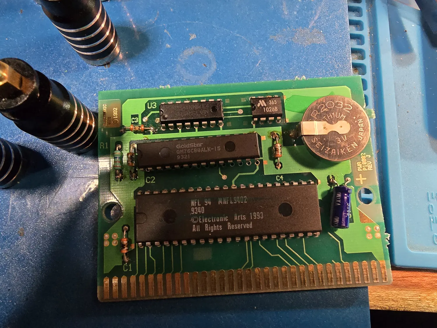
Cartridge save batteries
Not a console fault, but it lands on the same bench. Any Genesis cartridge with battery-backed saves carries a coin cell that is now three decades past its shelf life, and when it dies the game boots normally and simply forgets everything. Check how the cell is actually held before you reach for an iron. On some carts it is soldered; on others a metal tab retains it by friction even though the assembly does not look like a socket, and those come out without heat.
Recap and parts
The one rule to carry away: every in-scope Genesis and Mega Drive electrolytic is a through-hole radial, not surface-mount. Through-hole caps age far more gracefully than the surface-mount cans on a Game Gear, they rarely vent onto the board, and there is no SMD-corrosion trap on either console here. So a Genesis recap is usually preventative or symptom-driven, not the board-saving emergency it is on a Game Gear. Recap when you see audio buzz or weak sound, flickering power, or dim or rolling video, or when you are warrantying a resale unit. Do not sell a recap as a jailbar cure, since jailbars are a layout issue.
The one thing that will bite you: the caps are board-specific. Sega re-laid the board out every revision, so the designators and value splits do not carry across. Match the cap map or schematic for the exact board in hand.
- Buy the revision-matched kit for one-off work. Console5 sells a pre-matched kit for the exact board: an “IC series” kit covers Model 1 VA0 through VA6, and a “PC series” kit covers VA7 and Model 2 VA0/VA1/VA1.8. Right count, right values, name-brand parts, one SKU. A couple of per-revision gotchas: VA3 has the easy-to-miss 220 uF / 6.3 V VRAM cap on the underside; Model 2 VA1/VA1.8 have an encoder-dependent cap (CE14 is 220 uF on MB3514 boards but 10 uF on CXA1145/KA2195D boards, so check the encoder before ordering); and VA2/VA2.3 add two small odd values (2.2 uF and 22 uF at 50 V) that a VA0/VA1 kit will be missing.
- For à-la-carte, use Panasonic FR or Nichicon UPW. Both are low-ESR 105 C parts stocked at DigiKey and Mouser and a clear upgrade over the OEM caps. You can safely uprate voltage to standardize a kit (higher working voltage is always fine); never downrate. The two Model 1 audio-coupling caps (C61/C62, 1 uF / 50 V) are best as bipolar/non-polar types, though I will note that recommendation is single-sourced and the OEM schematic draws them polarized, so a polarized part there also works.
- 7805 regulators. Model 1 VA0 through VA6.8 carry two; VA7 and most Model 2 carry one. They run genuinely hot from the 9 to 10 V input, which is normal. A direct replacement is the STMicro L7805CV (keep the heatsink). A cool-running upgrade is the Recom R-78E5.0-1.0 switching module in the same TO-220 footprint, good on single-regulator boards and inside tight Model 2 shells, but keep it away from the analog audio and video section on an audiophile build (it is a switcher), and verify at least 1 A of headroom.
- A/V socket. The Model 1 8-pin DIN and Model 2 9-pin mini-DIN are non-standard Sega footprints, so DigiKey and Mouser do not stock a drop-in. Failures are almost always cold or cracked joints, so reflow first; replace only with a salvage socket or a specialty repro.
- Controller ports. The Sega port is a female DE-9. A generic right-angle PCB-mount DE-9 is electrically correct but the mounting footprint differs from Sega’s, so dry-fit before committing or pull a salvage port from a donor. Most “dead controller” faults are joints, so reflow the existing port before replacing.
- Cart slot, reset switch, volume slider. The cart slot is a cleaning job, not a replacement (IPA and light burnishing; no distributor equivalent). The Model 1 reset tact switch and volume slide-pot are common mechanical wear items with standard substitutes.
A sourcing note for a US bench: price DigiKey and Mouser first. After the current US import tariffs, LCSC usually loses on landed cost for small distributor-stocked parts (caps, 7805s, DE-9s) even where the unit price looks lower; it only wins on bulk reels you would import anyway.
If you would rather buy a console that has already had this work done, everything I restore is in the shop, and my general restoration and bench-testing method lives in the guides. I will link specific Genesis and Mega Drive service and mod listings here as those pages firm up.
Everything below this point is the same material as structured data: the per-revision cap maps, the parts I actually order, the pinouts I meter against, and the one-line numbers I look up. Each row carries its source and a confidence tag, so you can see where a figure came from and how hard it is. Expand any row for the detail.
Capacitor lists
The electrolytic map for each board revision, with the substitutes I fit. Two things to carry in: the designators do not survive a revision change, and a few revisions have no published list of their own. VA5, VA6.5 and VA6.8 are in that group. VA6.5 is a VA6 with the EXT port and line filters deleted, so the VA6 list is the right starting point minus the parts that went with those sections, but confirm against the board rather than trusting the count.
M1-VA0 Model 1 VA0: Japan launch, EDCLK on a daughterboard
Board p/n: 837-6656 (IC BD M5)
Main board 837-6656 — electrolytics
| Desig | Value | V | OEM p/n | Substitute | Note |
|---|---|---|---|---|---|
| C1 | 220µF | 16V | 220µF ≥16V: Panasonic EEU-FR1C221 (DigiKey 2433527) | main power filter ✓c5-m1,rs-caps | |
| C4 | 100µF | 10V | 100µF ≥16V: Panasonic EEU-FR1C101 (DigiKey 2433525) | ✓c5-m1,rs-caps | |
| C5 | 10µF | 16V | 10µF ≥16V: Panasonic EEU-FR1C100 or Nichicon UPW | ✓c5-m1,rs-caps | |
| C6 | 47µF | 10V | 47µF ≥25V: Panasonic EEU-FR1E470 covers every 47µF position uprated | ✓c5-m1,rs-caps | |
| C13 | 10µF | 16V | 10µF ≥16V: Panasonic EEU-FR1C100 or Nichicon UPW | ✓c5-m1,rs-caps | |
| C24 | 100µF | 10V | 100µF ≥16V: Panasonic EEU-FR1C101 (DigiKey 2433525) | ✓c5-m1,rs-caps | |
| C30 | 10µF | 16V | 10µF ≥16V: Panasonic EEU-FR1C100 or Nichicon UPW | ✓c5-m1,rs-caps | |
| C31 | 10µF | 16V | 10µF ≥16V: Panasonic EEU-FR1C100 or Nichicon UPW | ✓c5-m1,rs-caps | |
| C32 | 100µF | 10V | 100µF ≥16V: Panasonic EEU-FR1C101 (DigiKey 2433525) | ✓c5-m1,rs-caps | |
| C38 | 10µF | 16V | 10µF ≥16V: Panasonic EEU-FR1C100 or Nichicon UPW | ✓c5-m1,rs-caps | |
| C40 | 1µF | 50V | 1µF ≥50V; C61/C62 are the audio-coupling pair: sources say use bipolar/non-polar | ✓c5-m1,rs-caps | |
| C41 | 10µF | 10V | 10µF ≥16V: Panasonic EEU-FR1C100 or Nichicon UPW | ✓c5-m1,rs-caps | |
| C42 | 1µF | 50V | 1µF ≥50V; C61/C62 are the audio-coupling pair: sources say use bipolar/non-polar | ✓c5-m1,rs-caps | |
| C43 | 10µF | 16V | 10µF ≥16V: Panasonic EEU-FR1C100 or Nichicon UPW | ✓c5-m1,rs-caps | |
| C44 | 1µF | 50V | 1µF ≥50V; C61/C62 are the audio-coupling pair: sources say use bipolar/non-polar | ✓c5-m1,rs-caps | |
| C49 | 100µF | 10V | 100µF ≥16V: Panasonic EEU-FR1C101 (DigiKey 2433525) | ✓c5-m1,rs-caps | |
| C50 | 220µF | 10V | 220µF ≥16V: Panasonic EEU-FR1C221 (DigiKey 2433527) | ✓c5-m1,rs-caps | |
| C51 | 220µF | 10V | 220µF ≥16V: Panasonic EEU-FR1C221 (DigiKey 2433527) | ✓c5-m1,rs-caps | |
| C52 | 100µF | 10V | 100µF ≥16V: Panasonic EEU-FR1C101 (DigiKey 2433525) | ✓c5-m1,rs-caps | |
| C53 | 100µF | 10V | 100µF ≥16V: Panasonic EEU-FR1C101 (DigiKey 2433525) | ✓c5-m1,rs-caps | |
| C55 | 10µF | 16V | 10µF ≥16V: Panasonic EEU-FR1C100 or Nichicon UPW | ✓c5-m1,rs-caps | |
| C57 | 10µF | 16V | 10µF ≥16V: Panasonic EEU-FR1C100 or Nichicon UPW | ✓c5-m1,rs-caps | |
| C58 | 1µF | 50V | 1µF ≥50V; C61/C62 are the audio-coupling pair: sources say use bipolar/non-polar | ✓c5-m1,rs-caps | |
| C59 | 47µF | 10V | 47µF ≥25V: Panasonic EEU-FR1E470 covers every 47µF position uprated | ✓c5-m1,rs-caps | |
| C60 | 47µF | 10V | 47µF ≥25V: Panasonic EEU-FR1E470 covers every 47µF position uprated | ✓c5-m1,rs-caps | |
| C61 | 1µF | 50V | 1µF ≥50V; C61/C62 are the audio-coupling pair: sources say use bipolar/non-polar | audio-coupling pair: sources call for a bipolar/non-polar part here, single-sourced and the OEM sheet draws them polarized ✓c5-m1,rs-caps | |
| C62 | 1µF | 50V | 1µF ≥50V; C61/C62 are the audio-coupling pair: sources say use bipolar/non-polar | audio-coupling pair: sources call for a bipolar/non-polar part here, single-sourced and the OEM sheet draws them polarized ✓c5-m1,rs-caps | |
| C63 | 47µF | 10V | 47µF ≥25V: Panasonic EEU-FR1E470 covers every 47µF position uprated | ✓c5-m1,rs-caps | |
| C64 | 10µF | 16V | 10µF ≥16V: Panasonic EEU-FR1C100 or Nichicon UPW | ✓c5-m1,rs-caps | |
| C65 | 47µF | 10V | 47µF ≥25V: Panasonic EEU-FR1E470 covers every 47µF position uprated | ✓c5-m1,rs-caps | |
| C66 | 47µF | 10V | 47µF ≥25V: Panasonic EEU-FR1E470 covers every 47µF position uprated | ✓c5-m1,rs-caps | |
| C67 | 47µF | 10V | 47µF ≥25V: Panasonic EEU-FR1E470 covers every 47µF position uprated | ✓c5-m1,rs-caps | |
| C68 | 47µF | 10V | 47µF ≥25V: Panasonic EEU-FR1E470 covers every 47µF position uprated | ✓c5-m1,rs-caps | |
| C71 | 10µF | 16V | 10µF ≥16V: Panasonic EEU-FR1C100 or Nichicon UPW | ✓c5-m1,rs-caps | |
| C72 | 10µF | 16V | 10µF ≥16V: Panasonic EEU-FR1C100 or Nichicon UPW | ✓c5-m1,rs-caps | |
| C74 | 100µF | 10V | 100µF ≥16V: Panasonic EEU-FR1C101 (DigiKey 2433525) | ✓c5-m1,rs-caps |
EDCLK daughterboard 839-0231 — electrolytics
M1-VA1 Model 1 VA1: daughterboard folded into the 315-5339
Board p/n: 837-6832 (IC BD M5)
Main board 837-6832 — electrolytics
| Desig | Value | V | OEM p/n | Substitute | Note |
|---|---|---|---|---|---|
| C1 | 220µF | 16V | 220µF ≥16V: Panasonic EEU-FR1C221 (DigiKey 2433527) | main power filter ✓c5-m1,rs-caps | |
| C4 | 100µF | 10V | 100µF ≥16V: Panasonic EEU-FR1C101 (DigiKey 2433525) | ✓c5-m1,rs-caps | |
| C5 | 10µF | 16V | 10µF ≥16V: Panasonic EEU-FR1C100 or Nichicon UPW | ✓c5-m1,rs-caps | |
| C13 | 10µF | 16V | 10µF ≥16V: Panasonic EEU-FR1C100 or Nichicon UPW | ✓c5-m1,rs-caps | |
| C23 | 100µF | 10V | 100µF ≥16V: Panasonic EEU-FR1C101 (DigiKey 2433525) | ✓c5-m1,rs-caps | |
| C24 | 100µF | 10V | 100µF ≥16V: Panasonic EEU-FR1C101 (DigiKey 2433525) | ✓c5-m1,rs-caps | |
| C30 | 10µF | 16V | 10µF ≥16V: Panasonic EEU-FR1C100 or Nichicon UPW | ✓c5-m1,rs-caps | |
| C31 | 10µF | 16V | 10µF ≥16V: Panasonic EEU-FR1C100 or Nichicon UPW | ✓c5-m1,rs-caps | |
| C32 | 100µF | 10V | 100µF ≥16V: Panasonic EEU-FR1C101 (DigiKey 2433525) | ✓c5-m1,rs-caps | |
| C38 | 10µF | 16V | 10µF ≥16V: Panasonic EEU-FR1C100 or Nichicon UPW | ✓c5-m1,rs-caps | |
| C40 | 1µF | 50V | 1µF ≥50V; C61/C62 are the audio-coupling pair: sources say use bipolar/non-polar | ✓c5-m1,rs-caps | |
| C41 | 10µF | 10V | 10µF ≥16V: Panasonic EEU-FR1C100 or Nichicon UPW | ✓c5-m1,rs-caps | |
| C42 | 1µF | 50V | 1µF ≥50V; C61/C62 are the audio-coupling pair: sources say use bipolar/non-polar | ✓c5-m1,rs-caps | |
| C43 | 10µF | 16V | 10µF ≥16V: Panasonic EEU-FR1C100 or Nichicon UPW | ✓c5-m1,rs-caps | |
| C44 | 1µF | 50V | 1µF ≥50V; C61/C62 are the audio-coupling pair: sources say use bipolar/non-polar | ✓c5-m1,rs-caps | |
| C49 | 100µF | 10V | 100µF ≥16V: Panasonic EEU-FR1C101 (DigiKey 2433525) | ✓c5-m1,rs-caps | |
| C50 | 220µF | 10V | 220µF ≥16V: Panasonic EEU-FR1C221 (DigiKey 2433527) | ✓c5-m1,rs-caps | |
| C51 | 220µF | 10V | 220µF ≥16V: Panasonic EEU-FR1C221 (DigiKey 2433527) | ✓c5-m1,rs-caps | |
| C52 | 100µF | 10V | 100µF ≥16V: Panasonic EEU-FR1C101 (DigiKey 2433525) | ✓c5-m1,rs-caps | |
| C53 | 100µF | 10V | 100µF ≥16V: Panasonic EEU-FR1C101 (DigiKey 2433525) | ✓c5-m1,rs-caps | |
| C55 | 10µF | 16V | 10µF ≥16V: Panasonic EEU-FR1C100 or Nichicon UPW | ✓c5-m1,rs-caps | |
| C57 | 10µF | 16V | 10µF ≥16V: Panasonic EEU-FR1C100 or Nichicon UPW | ✓c5-m1,rs-caps | |
| C58 | 1µF | 50V | 1µF ≥50V; C61/C62 are the audio-coupling pair: sources say use bipolar/non-polar | ✓c5-m1,rs-caps | |
| C59 | 47µF | 16V | 47µF ≥25V: Panasonic EEU-FR1E470 covers every 47µF position uprated | ✓c5-m1,rs-caps | |
| C60 | 47µF | 16V | 47µF ≥25V: Panasonic EEU-FR1E470 covers every 47µF position uprated | ✓c5-m1,rs-caps | |
| C61 | 1µF | 50V | 1µF ≥50V; C61/C62 are the audio-coupling pair: sources say use bipolar/non-polar | audio-coupling pair: sources call for a bipolar/non-polar part here, single-sourced and the OEM sheet draws them polarized ✓c5-m1,rs-caps | |
| C62 | 1µF | 50V | 1µF ≥50V; C61/C62 are the audio-coupling pair: sources say use bipolar/non-polar | audio-coupling pair: sources call for a bipolar/non-polar part here, single-sourced and the OEM sheet draws them polarized ✓c5-m1,rs-caps | |
| C63 | 47µF | 16V | 47µF ≥25V: Panasonic EEU-FR1E470 covers every 47µF position uprated | ✓c5-m1,rs-caps | |
| C64 | 10µF | 16V | 10µF ≥16V: Panasonic EEU-FR1C100 or Nichicon UPW | ✓c5-m1,rs-caps | |
| C65 | 47µF | 16V | 47µF ≥25V: Panasonic EEU-FR1E470 covers every 47µF position uprated | ✓c5-m1,rs-caps | |
| C66 | 47µF | 16V | 47µF ≥25V: Panasonic EEU-FR1E470 covers every 47µF position uprated | ✓c5-m1,rs-caps | |
| C67 | 47µF | 16V | 47µF ≥25V: Panasonic EEU-FR1E470 covers every 47µF position uprated | ✓c5-m1,rs-caps | |
| C68 | 47µF | 16V | 47µF ≥25V: Panasonic EEU-FR1E470 covers every 47µF position uprated | ✓c5-m1,rs-caps | |
| C71 | 10µF | 16V | 10µF ≥16V: Panasonic EEU-FR1C100 or Nichicon UPW | ✓c5-m1,rs-caps | |
| C72 | 10µF | 16V | 10µF ≥16V: Panasonic EEU-FR1C100 or Nichicon UPW | ✓c5-m1,rs-caps | |
| C74 | 100µF | 10V | 100µF ≥16V: Panasonic EEU-FR1C101 (DigiKey 2433525) | ✓c5-m1,rs-caps | |
| C79 | 100µF | 16V | 100µF ≥16V: Panasonic EEU-FR1C101 (DigiKey 2433525) | ✓c5-m1,rs-caps | |
| JPx | 47µF | 16V | 47µF ≥25V: Panasonic EEU-FR1E470 covers every 47µF position uprated | sits at the factory jumper block ✓c5-m1,rs-caps |
M1-VA2 Model 1 VA2: first North American board; 315-5345 fixes the DMA-refresh glitch
Board p/n: 837-6955 (JP) · 837-6992 (NA)
JP board 837-6955 — electrolytics
| Desig | Value | V | OEM p/n | Substitute | Note |
|---|---|---|---|---|---|
| C1 | 220µF | 16V | 220µF ≥16V: Panasonic EEU-FR1C221 (DigiKey 2433527) | main power filter ✓c5-m1,rs-caps | |
| C4 | 100µF | 10V | 100µF ≥16V: Panasonic EEU-FR1C101 (DigiKey 2433525) | ✓c5-m1,rs-caps | |
| C5 | 10µF | 25V | 10µF ≥16V: Panasonic EEU-FR1C100 or Nichicon UPW | ✓c5-m1,rs-caps | |
| C13 | 10µF | 25V | 10µF ≥16V: Panasonic EEU-FR1C100 or Nichicon UPW | ✓c5-m1,rs-caps | |
| C23 | 100µF | 10V | 100µF ≥16V: Panasonic EEU-FR1C101 (DigiKey 2433525) | ✓c5-m1,rs-caps | |
| C24 | 100µF | 10V | 100µF ≥16V: Panasonic EEU-FR1C101 (DigiKey 2433525) | ✓c5-m1,rs-caps | |
| C30 | 10µF | 25V | 10µF ≥16V: Panasonic EEU-FR1C100 or Nichicon UPW | ✓c5-m1,rs-caps | |
| C31 | 10µF | 25V | 10µF ≥16V: Panasonic EEU-FR1C100 or Nichicon UPW | ✓c5-m1,rs-caps | |
| C32 | 220µF | 10V | 220µF ≥16V: Panasonic EEU-FR1C221 (DigiKey 2433527) | ✓c5-m1,rs-caps | |
| C38 | 10µF | 25V | 10µF ≥16V: Panasonic EEU-FR1C100 or Nichicon UPW | ✓c5-m1,rs-caps | |
| C40 | 1µF | 50V | 1µF ≥50V; C61/C62 are the audio-coupling pair: sources say use bipolar/non-polar | ✓c5-m1,rs-caps | |
| C41 | 10µF | 25V | 10µF ≥16V: Panasonic EEU-FR1C100 or Nichicon UPW | ✓c5-m1,rs-caps | |
| C42 | 1µF | 50V | 1µF ≥50V; C61/C62 are the audio-coupling pair: sources say use bipolar/non-polar | ✓c5-m1,rs-caps | |
| C43 | 10µF | 25V | 10µF ≥16V: Panasonic EEU-FR1C100 or Nichicon UPW | ✓c5-m1,rs-caps | |
| C44 | 1µF | 50V | 1µF ≥50V; C61/C62 are the audio-coupling pair: sources say use bipolar/non-polar | ✓c5-m1,rs-caps | |
| C49 | 100µF | 10V | 100µF ≥16V: Panasonic EEU-FR1C101 (DigiKey 2433525) | ✓c5-m1,rs-caps | |
| C50 | 220µF | 10V | 220µF ≥16V: Panasonic EEU-FR1C221 (DigiKey 2433527) | ✓c5-m1,rs-caps | |
| C51 | 220µF | 10V | 220µF ≥16V: Panasonic EEU-FR1C221 (DigiKey 2433527) | ✓c5-m1,rs-caps | |
| C52 | 100µF | 10V | 100µF ≥16V: Panasonic EEU-FR1C101 (DigiKey 2433525) | ✓c5-m1,rs-caps | |
| C53 | 100µF | 10V | 100µF ≥16V: Panasonic EEU-FR1C101 (DigiKey 2433525) | ✓c5-m1,rs-caps | |
| C55 | 10µF | 25V | 10µF ≥16V: Panasonic EEU-FR1C100 or Nichicon UPW | ✓c5-m1,rs-caps | |
| C57 | 10µF | 25V | 10µF ≥16V: Panasonic EEU-FR1C100 or Nichicon UPW | ✓c5-m1,rs-caps | |
| C58 | 1µF | 50V | 1µF ≥50V; C61/C62 are the audio-coupling pair: sources say use bipolar/non-polar | ✓c5-m1,rs-caps | |
| C59 | 47µF | 16V | 47µF ≥25V: Panasonic EEU-FR1E470 covers every 47µF position uprated | ✓c5-m1,rs-caps | |
| C60 | 47µF | 16V | 47µF ≥25V: Panasonic EEU-FR1E470 covers every 47µF position uprated | ✓c5-m1,rs-caps | |
| C61 | 1µF | 50V | 1µF ≥50V; C61/C62 are the audio-coupling pair: sources say use bipolar/non-polar | audio-coupling pair: sources call for a bipolar/non-polar part here, single-sourced and the OEM sheet draws them polarized ✓c5-m1,rs-caps | |
| C62 | 1µF | 50V | 1µF ≥50V; C61/C62 are the audio-coupling pair: sources say use bipolar/non-polar | audio-coupling pair: sources call for a bipolar/non-polar part here, single-sourced and the OEM sheet draws them polarized ✓c5-m1,rs-caps | |
| C63 | 47µF | 16V | 47µF ≥25V: Panasonic EEU-FR1E470 covers every 47µF position uprated | ✓c5-m1,rs-caps | |
| C64 | 10µF | 25V | 10µF ≥16V: Panasonic EEU-FR1C100 or Nichicon UPW | ✓c5-m1,rs-caps | |
| C65 | 47µF | 16V | 47µF ≥25V: Panasonic EEU-FR1E470 covers every 47µF position uprated | ✓c5-m1,rs-caps | |
| C66 | 47µF | 16V | 47µF ≥25V: Panasonic EEU-FR1E470 covers every 47µF position uprated | ✓c5-m1,rs-caps | |
| C67 | 47µF | 16V | 47µF ≥25V: Panasonic EEU-FR1E470 covers every 47µF position uprated | ✓c5-m1,rs-caps | |
| C68 | 47µF | 16V | 47µF ≥25V: Panasonic EEU-FR1E470 covers every 47µF position uprated | ✓c5-m1,rs-caps | |
| C71 | 10µF | 25V | 10µF ≥16V: Panasonic EEU-FR1C100 or Nichicon UPW | ✓c5-m1,rs-caps | |
| C72 | 10µF | 25V | 10µF ≥16V: Panasonic EEU-FR1C100 or Nichicon UPW | ✓c5-m1,rs-caps | |
| C74 | 100µF | 10V | 100µF ≥16V: Panasonic EEU-FR1C101 (DigiKey 2433525) | ✓c5-m1,rs-caps | |
| C79 | 100µF | 16V | 100µF ≥16V: Panasonic EEU-FR1C101 (DigiKey 2433525) | ✓c5-m1,rs-caps |
NA board 837-6992 (adds the internal RF modulator) — electrolytics
| Desig | Value | V | OEM p/n | Substitute | Note |
|---|---|---|---|---|---|
| C1 | 220µF | 16V | 220µF ≥16V: Panasonic EEU-FR1C221 (DigiKey 2433527) | main power filter ✓c5-m1,rs-caps | |
| C4 | 100µF | 10V | 100µF ≥16V: Panasonic EEU-FR1C101 (DigiKey 2433525) | ✓c5-m1,rs-caps | |
| C5 | 10µF | 16V | 10µF ≥16V: Panasonic EEU-FR1C100 or Nichicon UPW | ✓c5-m1,rs-caps | |
| C13 | 10µF | 16V | 10µF ≥16V: Panasonic EEU-FR1C100 or Nichicon UPW | ✓c5-m1,rs-caps | |
| C23 | 100µF | 10V | 100µF ≥16V: Panasonic EEU-FR1C101 (DigiKey 2433525) | ✓c5-m1,rs-caps | |
| C24 | 100µF | 10V | 100µF ≥16V: Panasonic EEU-FR1C101 (DigiKey 2433525) | ✓c5-m1,rs-caps | |
| C30 | 10µF | 16V | 10µF ≥16V: Panasonic EEU-FR1C100 or Nichicon UPW | console5 has one report of C30/C60 swapped at the factory: fit the listed value, not what came out ✓c5-m1,rs-caps | |
| C31 | 10µF | 16V | 10µF ≥16V: Panasonic EEU-FR1C100 or Nichicon UPW | ✓c5-m1,rs-caps | |
| C32 | 220µF | 10V | 220µF ≥16V: Panasonic EEU-FR1C221 (DigiKey 2433527) | ✓c5-m1,rs-caps | |
| C38 | 10µF | 16V | 10µF ≥16V: Panasonic EEU-FR1C100 or Nichicon UPW | ✓c5-m1,rs-caps | |
| C40 | 1µF | 50V | 1µF ≥50V; C61/C62 are the audio-coupling pair: sources say use bipolar/non-polar | ✓c5-m1,rs-caps | |
| C41 | 10µF | 10V | 10µF ≥16V: Panasonic EEU-FR1C100 or Nichicon UPW | ✓c5-m1,rs-caps | |
| C42 | 1µF | 50V | 1µF ≥50V; C61/C62 are the audio-coupling pair: sources say use bipolar/non-polar | ✓c5-m1,rs-caps | |
| C43 | 10µF | 16V | 10µF ≥16V: Panasonic EEU-FR1C100 or Nichicon UPW | ✓c5-m1,rs-caps | |
| C44 | 1µF | 50V | 1µF ≥50V; C61/C62 are the audio-coupling pair: sources say use bipolar/non-polar | ✓c5-m1,rs-caps | |
| C49 | 100µF | 10V | 100µF ≥16V: Panasonic EEU-FR1C101 (DigiKey 2433525) | ✓c5-m1,rs-caps | |
| C50 | 220µF | 10V | 220µF ≥16V: Panasonic EEU-FR1C221 (DigiKey 2433527) | ✓c5-m1,rs-caps | |
| C51 | 220µF | 10V | 220µF ≥16V: Panasonic EEU-FR1C221 (DigiKey 2433527) | ✓c5-m1,rs-caps | |
| C52 | 100µF | 10V | 100µF ≥16V: Panasonic EEU-FR1C101 (DigiKey 2433525) | ✓c5-m1,rs-caps | |
| C53 | 100µF | 10V | 100µF ≥16V: Panasonic EEU-FR1C101 (DigiKey 2433525) | ✓c5-m1,rs-caps | |
| C55 | 10µF | 16V | 10µF ≥16V: Panasonic EEU-FR1C100 or Nichicon UPW | ✓c5-m1,rs-caps | |
| C57 | 10µF | 16V | 10µF ≥16V: Panasonic EEU-FR1C100 or Nichicon UPW | ✓c5-m1,rs-caps | |
| C58 | 1µF | 50V | 1µF ≥50V; C61/C62 are the audio-coupling pair: sources say use bipolar/non-polar | ✓c5-m1,rs-caps | |
| C59 | 47µF | 16V | 47µF ≥25V: Panasonic EEU-FR1E470 covers every 47µF position uprated | ✓c5-m1,rs-caps | |
| C60 | 47µF | 16V | 47µF ≥25V: Panasonic EEU-FR1E470 covers every 47µF position uprated | see the C30 note: one reported factory swap ✓c5-m1,rs-caps | |
| C61 | 1µF | 50V | 1µF ≥50V; C61/C62 are the audio-coupling pair: sources say use bipolar/non-polar | audio-coupling pair: sources call for a bipolar/non-polar part here, single-sourced and the OEM sheet draws them polarized ✓c5-m1,rs-caps | |
| C62 | 1µF | 50V | 1µF ≥50V; C61/C62 are the audio-coupling pair: sources say use bipolar/non-polar | audio-coupling pair: sources call for a bipolar/non-polar part here, single-sourced and the OEM sheet draws them polarized ✓c5-m1,rs-caps | |
| C63 | 47µF | 16V | 47µF ≥25V: Panasonic EEU-FR1E470 covers every 47µF position uprated | ✓c5-m1,rs-caps | |
| C64 | 10µF | 16V | 10µF ≥16V: Panasonic EEU-FR1C100 or Nichicon UPW | ✓c5-m1,rs-caps | |
| C65 | 47µF | 10V | 47µF ≥25V: Panasonic EEU-FR1E470 covers every 47µF position uprated | ✓c5-m1,rs-caps | |
| C66 | 47µF | 10V | 47µF ≥25V: Panasonic EEU-FR1E470 covers every 47µF position uprated | ✓c5-m1,rs-caps | |
| C67 | 47µF | 10V | 47µF ≥25V: Panasonic EEU-FR1E470 covers every 47µF position uprated | ✓c5-m1,rs-caps | |
| C68 | 47µF | 10V | 47µF ≥25V: Panasonic EEU-FR1E470 covers every 47µF position uprated | ✓c5-m1,rs-caps | |
| C71 | 10µF | 16V | 10µF ≥16V: Panasonic EEU-FR1C100 or Nichicon UPW | ✓c5-m1,rs-caps | |
| C72 | 10µF | 16V | 10µF ≥16V: Panasonic EEU-FR1C100 or Nichicon UPW | ✓c5-m1,rs-caps | |
| C74 | 100µF | 10V | 100µF ≥16V: Panasonic EEU-FR1C101 (DigiKey 2433525) | ✓c5-m1,rs-caps | |
| C79 | 100µF | 16V | 100µF ≥16V: Panasonic EEU-FR1C101 (DigiKey 2433525) | ✓c5-m1,rs-caps | |
| C86 | 100µF | 10V | 100µF ≥16V: Panasonic EEU-FR1C101 (DigiKey 2433525) | ✓c5-m1,rs-caps | |
| JPx | 47µF | 10V | 47µF ≥25V: Panasonic EEU-FR1E470 covers every 47µF position uprated | sits at the factory jumper block ✓c5-m1,rs-caps |
M1-VA3 Model 1 VA3: arbiter and clock generator merge; the audio baseline
Board p/n: 837-7071 (IC BD M5 USA)
Main board 837-7071 — electrolytics
| Desig | Value | V | OEM p/n | Substitute | Note |
|---|---|---|---|---|---|
| C1 | 220µF | 16V | 220µF ≥16V: Panasonic EEU-FR1C221 (DigiKey 2433527) | main power filter ✓c5-m1,rs-caps | |
| C4 | 100µF | 10V | 100µF ≥16V: Panasonic EEU-FR1C101 (DigiKey 2433525) | ✓c5-m1,rs-caps | |
| C5 | 10µF | 16V | 10µF ≥16V: Panasonic EEU-FR1C100 or Nichicon UPW | ✓c5-m1,rs-caps | |
| C13 | 10µF | 16V | 10µF ≥16V: Panasonic EEU-FR1C100 or Nichicon UPW | ✓c5-m1,rs-caps | |
| C23 | 100µF | 10V | 100µF ≥16V: Panasonic EEU-FR1C101 (DigiKey 2433525) | ✓c5-m1,rs-caps | |
| C24 | 100µF | 10V | 100µF ≥16V: Panasonic EEU-FR1C101 (DigiKey 2433525) | ✓c5-m1,rs-caps | |
| C30 | 10µF | 16V | 10µF ≥16V: Panasonic EEU-FR1C100 or Nichicon UPW | ✓c5-m1,rs-caps | |
| C31 | 10µF | 16V | 10µF ≥16V: Panasonic EEU-FR1C100 or Nichicon UPW | ✓c5-m1,rs-caps | |
| C32 | 220µF | 10V | 220µF ≥16V: Panasonic EEU-FR1C221 (DigiKey 2433527) | ✓c5-m1,rs-caps | |
| C38 | 10µF | 16V | 10µF ≥16V: Panasonic EEU-FR1C100 or Nichicon UPW | ✓c5-m1,rs-caps | |
| C40 | 1µF | 50V | 1µF ≥50V; C61/C62 are the audio-coupling pair: sources say use bipolar/non-polar | ✓c5-m1,rs-caps | |
| C41 | 10µF | 25V | 10µF ≥16V: Panasonic EEU-FR1C100 or Nichicon UPW | ✓c5-m1,rs-caps | |
| C42 | 1µF | 50V | 1µF ≥50V; C61/C62 are the audio-coupling pair: sources say use bipolar/non-polar | ✓c5-m1,rs-caps | |
| C43 | 10µF | 25V | 10µF ≥16V: Panasonic EEU-FR1C100 or Nichicon UPW | ✓c5-m1,rs-caps | |
| C44 | 1µF | 50V | 1µF ≥50V; C61/C62 are the audio-coupling pair: sources say use bipolar/non-polar | ✓c5-m1,rs-caps | |
| C49 | 100µF | 10V | 100µF ≥16V: Panasonic EEU-FR1C101 (DigiKey 2433525) | ✓c5-m1,rs-caps | |
| C50 | 220µF | 10V | 220µF ≥16V: Panasonic EEU-FR1C221 (DigiKey 2433527) | ✓c5-m1,rs-caps | |
| C51 | 220µF | 10V | 220µF ≥16V: Panasonic EEU-FR1C221 (DigiKey 2433527) | ✓c5-m1,rs-caps | |
| C52 | 100µF | 10V | 100µF ≥16V: Panasonic EEU-FR1C101 (DigiKey 2433525) | ✓c5-m1,rs-caps | |
| C53 | 100µF | 10V | 100µF ≥16V: Panasonic EEU-FR1C101 (DigiKey 2433525) | ✓c5-m1,rs-caps | |
| C55 | 10µF | 25V | 10µF ≥16V: Panasonic EEU-FR1C100 or Nichicon UPW | ✓c5-m1,rs-caps | |
| C57 | 10µF | 16V | 10µF ≥16V: Panasonic EEU-FR1C100 or Nichicon UPW | ✓c5-m1,rs-caps | |
| C58 | 1µF | 50V | 1µF ≥50V; C61/C62 are the audio-coupling pair: sources say use bipolar/non-polar | ✓c5-m1,rs-caps | |
| C59 | 47µF | 16V | 47µF ≥25V: Panasonic EEU-FR1E470 covers every 47µF position uprated | ✓c5-m1,rs-caps | |
| C60 | 47µF | 16V | 47µF ≥25V: Panasonic EEU-FR1E470 covers every 47µF position uprated | ✓c5-m1,rs-caps | |
| C61 | 1µF | 50V | 1µF ≥50V; C61/C62 are the audio-coupling pair: sources say use bipolar/non-polar | audio-coupling pair: sources call for a bipolar/non-polar part here, single-sourced and the OEM sheet draws them polarized ✓c5-m1,rs-caps | |
| C62 | 1µF | 50V | 1µF ≥50V; C61/C62 are the audio-coupling pair: sources say use bipolar/non-polar | audio-coupling pair: sources call for a bipolar/non-polar part here, single-sourced and the OEM sheet draws them polarized ✓c5-m1,rs-caps | |
| C63 | 47µF | 16V | 47µF ≥25V: Panasonic EEU-FR1E470 covers every 47µF position uprated | ✓c5-m1,rs-caps | |
| C64 | 10µF | 25V | 10µF ≥16V: Panasonic EEU-FR1C100 or Nichicon UPW | ✓c5-m1,rs-caps | |
| C65 | 47µF | 16V | 47µF ≥25V: Panasonic EEU-FR1E470 covers every 47µF position uprated | ✓c5-m1,rs-caps | |
| C66 | 47µF | 16V | 47µF ≥25V: Panasonic EEU-FR1E470 covers every 47µF position uprated | ✓c5-m1,rs-caps | |
| C67 | 47µF | 16V | 47µF ≥25V: Panasonic EEU-FR1E470 covers every 47µF position uprated | ✓c5-m1,rs-caps | |
| C68 | 47µF | 16V | 47µF ≥25V: Panasonic EEU-FR1E470 covers every 47µF position uprated | ✓c5-m1,rs-caps | |
| C71 | 10µF | 16V | 10µF ≥16V: Panasonic EEU-FR1C100 or Nichicon UPW | ✓c5-m1,rs-caps | |
| C72 | 10µF | 16V | 10µF ≥16V: Panasonic EEU-FR1C100 or Nichicon UPW | ✓c5-m1,rs-caps | |
| C74 | 100µF | 10V | 100µF ≥16V: Panasonic EEU-FR1C101 (DigiKey 2433525) | ✓c5-m1,rs-caps | |
| C79 | 100µF | 16V | 100µF ≥16V: Panasonic EEU-FR1C101 (DigiKey 2433525) | ✓c5-m1,rs-caps | |
| C86 | 100µF | 10V | 100µF ≥16V: Panasonic EEU-FR1C101 (DigiKey 2433525) | ✓c5-m1,rs-caps | |
| JPx | 47µF | 16V | 47µF ≥25V: Panasonic EEU-FR1E470 covers every 47µF position uprated | sits at the factory jumper block ✓c5-m1,rs-caps | |
| BOT | 220µF | 6.3V | 220µF ≥16V: Panasonic EEU-FR1C221 (DigiKey 2433527) | UNDERSIDE: sits on the board bottom on the VRAM VCC pin; the one I have watched people miss on a top-side recap ✓c5-m1,rs-caps |
M1-VA4 Model 1 VA4: first Asia/PAL/Korea board; video circuit rearranged
Board p/n: 171-5872-20 (PAL/Asia) · 837-7138 (JP/KR)
Main board 171-5872-20 (PAL VA4) — electrolytics
| Desig | Value | V | OEM p/n | Substitute | Note |
|---|---|---|---|---|---|
| C1 | 220µF | 16V | 220µF ≥16V: Panasonic EEU-FR1C221 (DigiKey 2433527) | main power filter ✓c5-m1,rs-caps | |
| C4 | 100µF | 10V | 100µF ≥16V: Panasonic EEU-FR1C101 (DigiKey 2433525) | ✓c5-m1,rs-caps | |
| C5 | 10µF | 16V | 10µF ≥16V: Panasonic EEU-FR1C100 or Nichicon UPW | ✓c5-m1,rs-caps | |
| C13 | 10µF | 16V | 10µF ≥16V: Panasonic EEU-FR1C100 or Nichicon UPW | ✓c5-m1,rs-caps | |
| C23 | 100µF | 10V | 100µF ≥16V: Panasonic EEU-FR1C101 (DigiKey 2433525) | ✓c5-m1,rs-caps | |
| C24 | 100µF | 10V | 100µF ≥16V: Panasonic EEU-FR1C101 (DigiKey 2433525) | ✓c5-m1,rs-caps | |
| C30 | 10µF | 16V | 10µF ≥16V: Panasonic EEU-FR1C100 or Nichicon UPW | ✓c5-m1,rs-caps | |
| C31 | 10µF | 16V | 10µF ≥16V: Panasonic EEU-FR1C100 or Nichicon UPW | ✓c5-m1,rs-caps | |
| C32 | 220µF | 10V | 220µF ≥16V: Panasonic EEU-FR1C221 (DigiKey 2433527) | ✓c5-m1,rs-caps | |
| C38 | 10µF | 16V | 10µF ≥16V: Panasonic EEU-FR1C100 or Nichicon UPW | ✓c5-m1,rs-caps | |
| C40 | 1µF | 50V | 1µF ≥50V; C61/C62 are the audio-coupling pair: sources say use bipolar/non-polar | ✓c5-m1,rs-caps | |
| C41 | 10µF | 16V | 10µF ≥16V: Panasonic EEU-FR1C100 or Nichicon UPW | ✓c5-m1,rs-caps | |
| C42 | 1µF | 50V | 1µF ≥50V; C61/C62 are the audio-coupling pair: sources say use bipolar/non-polar | ✓c5-m1,rs-caps | |
| C43 | 10µF | 16V | 10µF ≥16V: Panasonic EEU-FR1C100 or Nichicon UPW | ✓c5-m1,rs-caps | |
| C44 | 1µF | 50V | 1µF ≥50V; C61/C62 are the audio-coupling pair: sources say use bipolar/non-polar | ✓c5-m1,rs-caps | |
| C49 | 100µF | 10V | 100µF ≥16V: Panasonic EEU-FR1C101 (DigiKey 2433525) | ✓c5-m1,rs-caps | |
| C50 | 220µF | 10V | 220µF ≥16V: Panasonic EEU-FR1C221 (DigiKey 2433527) | ✓c5-m1,rs-caps | |
| C51 | 220µF | 10V | 220µF ≥16V: Panasonic EEU-FR1C221 (DigiKey 2433527) | ✓c5-m1,rs-caps | |
| C52 | 100µF | 10V | 100µF ≥16V: Panasonic EEU-FR1C101 (DigiKey 2433525) | ✓c5-m1,rs-caps | |
| C53 | 100µF | 10V | 100µF ≥16V: Panasonic EEU-FR1C101 (DigiKey 2433525) | ✓c5-m1,rs-caps | |
| C55 | 10µF | 16V | 10µF ≥16V: Panasonic EEU-FR1C100 or Nichicon UPW | ✓c5-m1,rs-caps | |
| C57 | 10µF | 16V | 10µF ≥16V: Panasonic EEU-FR1C100 or Nichicon UPW | ✓c5-m1,rs-caps | |
| C58 | 1µF | 50V | 1µF ≥50V; C61/C62 are the audio-coupling pair: sources say use bipolar/non-polar | ✓c5-m1,rs-caps | |
| C59 | 47µF | 10V | 47µF ≥25V: Panasonic EEU-FR1E470 covers every 47µF position uprated | ✓c5-m1,rs-caps | |
| C60 | 47µF | 10V | 47µF ≥25V: Panasonic EEU-FR1E470 covers every 47µF position uprated | ✓c5-m1,rs-caps | |
| C61 | 1µF | 50V | 1µF ≥50V; C61/C62 are the audio-coupling pair: sources say use bipolar/non-polar | audio-coupling pair: sources call for a bipolar/non-polar part here, single-sourced and the OEM sheet draws them polarized ✓c5-m1,rs-caps | |
| C62 | 1µF | 50V | 1µF ≥50V; C61/C62 are the audio-coupling pair: sources say use bipolar/non-polar | audio-coupling pair: sources call for a bipolar/non-polar part here, single-sourced and the OEM sheet draws them polarized ✓c5-m1,rs-caps | |
| C63 | 47µF | 10V | 47µF ≥25V: Panasonic EEU-FR1E470 covers every 47µF position uprated | ✓c5-m1,rs-caps | |
| C64 | 10µF | 16V | 10µF ≥16V: Panasonic EEU-FR1C100 or Nichicon UPW | ✓c5-m1,rs-caps | |
| C65 | 47µF | 10V | 47µF ≥25V: Panasonic EEU-FR1E470 covers every 47µF position uprated | ✓c5-m1,rs-caps | |
| C66 | 47µF | 10V | 47µF ≥25V: Panasonic EEU-FR1E470 covers every 47µF position uprated | ✓c5-m1,rs-caps | |
| C67 | 47µF | 10V | 47µF ≥25V: Panasonic EEU-FR1E470 covers every 47µF position uprated | ✓c5-m1,rs-caps | |
| C68 | 47µF | 10V | 47µF ≥25V: Panasonic EEU-FR1E470 covers every 47µF position uprated | ✓c5-m1,rs-caps | |
| C71 | 10µF | 16V | 10µF ≥16V: Panasonic EEU-FR1C100 or Nichicon UPW | ✓c5-m1,rs-caps | |
| C72 | 10µF | 16V | 10µF ≥16V: Panasonic EEU-FR1C100 or Nichicon UPW | ✓c5-m1,rs-caps | |
| C74 | 100µF | 10V | 100µF ≥16V: Panasonic EEU-FR1C101 (DigiKey 2433525) | ✓c5-m1,rs-caps | |
| C79 | 100µF | 16V | 100µF ≥16V: Panasonic EEU-FR1C101 (DigiKey 2433525) | ✓c5-m1,rs-caps | |
| C86 | 100µF | 10V | 100µF ≥16V: Panasonic EEU-FR1C101 (DigiKey 2433525) | ✓c5-m1,rs-caps |
M1-VA5 Model 1 VA5: Japan only; I/O and arbiter merge into the 315-5402
Board p/n: 171-5963
M1-VA6 Model 1 VA6: first TMSS board (315-5433); last with the EXT port in most markets
Board p/n: 171-5963-10 (NA) · 171-5963-30 (Asia/PAL)
Main board 171-5963-10 / -30 — electrolytics
| Desig | Value | V | OEM p/n | Substitute | Note |
|---|---|---|---|---|---|
| C1 | 220µF | 16V | 220µF ≥16V: Panasonic EEU-FR1C221 (DigiKey 2433527) | main power filter ✓c5-m1,rs-caps | |
| C4 | 100µF | 10V | 100µF ≥16V: Panasonic EEU-FR1C101 (DigiKey 2433525) | ✓c5-m1,rs-caps | |
| C5 | 10µF | 16V | 10µF ≥16V: Panasonic EEU-FR1C100 or Nichicon UPW | ✓c5-m1,rs-caps | |
| C13 | 10µF | 16V | 10µF ≥16V: Panasonic EEU-FR1C100 or Nichicon UPW | ✓c5-m1,rs-caps | |
| C23 | 100µF | 10V | 100µF ≥16V: Panasonic EEU-FR1C101 (DigiKey 2433525) | ✓c5-m1,rs-caps | |
| C24 | 100µF | 10V | 100µF ≥16V: Panasonic EEU-FR1C101 (DigiKey 2433525) | ✓c5-m1,rs-caps | |
| C30 | 10µF | 16V | 10µF ≥16V: Panasonic EEU-FR1C100 or Nichicon UPW | the cap consolemods says the PAL-only VA6.8 leaves unpopulated: see the schematic facts ✓c5-m1,rs-caps | |
| C31 | 10µF | 16V | 10µF ≥16V: Panasonic EEU-FR1C100 or Nichicon UPW | ✓c5-m1,rs-caps | |
| C32 | 220µF | 10V | 220µF ≥16V: Panasonic EEU-FR1C221 (DigiKey 2433527) | ✓c5-m1,rs-caps | |
| C38 | 10µF | 16V | 10µF ≥16V: Panasonic EEU-FR1C100 or Nichicon UPW | ✓c5-m1,rs-caps | |
| C40 | 1µF | 50V | 1µF ≥50V; C61/C62 are the audio-coupling pair: sources say use bipolar/non-polar | ✓c5-m1,rs-caps | |
| C41 | 10µF | 16V | 10µF ≥16V: Panasonic EEU-FR1C100 or Nichicon UPW | ✓c5-m1,rs-caps | |
| C42 | 1µF | 50V | 1µF ≥50V; C61/C62 are the audio-coupling pair: sources say use bipolar/non-polar | ✓c5-m1,rs-caps | |
| C43 | 10µF | 16V | 10µF ≥16V: Panasonic EEU-FR1C100 or Nichicon UPW | ✓c5-m1,rs-caps | |
| C44 | 1µF | 50V | 1µF ≥50V; C61/C62 are the audio-coupling pair: sources say use bipolar/non-polar | ✓c5-m1,rs-caps | |
| C49 | 100µF | 10V | 100µF ≥16V: Panasonic EEU-FR1C101 (DigiKey 2433525) | ✓c5-m1,rs-caps | |
| C50 | 220µF | 10V | 220µF ≥16V: Panasonic EEU-FR1C221 (DigiKey 2433527) | ✓c5-m1,rs-caps | |
| C51 | 220µF | 10V | 220µF ≥16V: Panasonic EEU-FR1C221 (DigiKey 2433527) | ✓c5-m1,rs-caps | |
| C52 | 100µF | 10V | 100µF ≥16V: Panasonic EEU-FR1C101 (DigiKey 2433525) | ✓c5-m1,rs-caps | |
| C53 | 100µF | 10V | 100µF ≥16V: Panasonic EEU-FR1C101 (DigiKey 2433525) | ✓c5-m1,rs-caps | |
| C55 | 10µF | 16V | 10µF ≥16V: Panasonic EEU-FR1C100 or Nichicon UPW | ✓c5-m1,rs-caps | |
| C57 | 10µF | 16V | 10µF ≥16V: Panasonic EEU-FR1C100 or Nichicon UPW | ✓c5-m1,rs-caps | |
| C58 | 1µF | 50V | 1µF ≥50V; C61/C62 are the audio-coupling pair: sources say use bipolar/non-polar | ✓c5-m1,rs-caps | |
| C59 | 47µF | 10V | 47µF ≥25V: Panasonic EEU-FR1E470 covers every 47µF position uprated | ✓c5-m1,rs-caps | |
| C60 | 47µF | 10V | 47µF ≥25V: Panasonic EEU-FR1E470 covers every 47µF position uprated | ✓c5-m1,rs-caps | |
| C61 | 1µF | 50V | 1µF ≥50V; C61/C62 are the audio-coupling pair: sources say use bipolar/non-polar | audio-coupling pair: sources call for a bipolar/non-polar part here, single-sourced and the OEM sheet draws them polarized ✓c5-m1,rs-caps | |
| C62 | 1µF | 50V | 1µF ≥50V; C61/C62 are the audio-coupling pair: sources say use bipolar/non-polar | audio-coupling pair: sources call for a bipolar/non-polar part here, single-sourced and the OEM sheet draws them polarized ✓c5-m1,rs-caps | |
| C63 | 47µF | 10V | 47µF ≥25V: Panasonic EEU-FR1E470 covers every 47µF position uprated | ✓c5-m1,rs-caps | |
| C64 | 10µF | 16V | 10µF ≥16V: Panasonic EEU-FR1C100 or Nichicon UPW | ✓c5-m1,rs-caps | |
| C65 | 47µF | 10V | 47µF ≥25V: Panasonic EEU-FR1E470 covers every 47µF position uprated | ✓c5-m1,rs-caps | |
| C66 | 47µF | 10V | 47µF ≥25V: Panasonic EEU-FR1E470 covers every 47µF position uprated | ✓c5-m1,rs-caps | |
| C68 | 47µF | 10V | 47µF ≥25V: Panasonic EEU-FR1E470 covers every 47µF position uprated | ✓c5-m1,rs-caps | |
| C71 | 10µF | 16V | 10µF ≥16V: Panasonic EEU-FR1C100 or Nichicon UPW | ✓c5-m1,rs-caps | |
| C72 | 10µF | 16V | 10µF ≥16V: Panasonic EEU-FR1C100 or Nichicon UPW | ✓c5-m1,rs-caps | |
| C74 | 100µF | 10V | 100µF ≥16V: Panasonic EEU-FR1C101 (DigiKey 2433525) | ✓c5-m1,rs-caps | |
| C79 | 100µF | 16V | 100µF ≥16V: Panasonic EEU-FR1C101 (DigiKey 2433525) | ✓c5-m1,rs-caps | |
| C86 | 100µF | 10V | 100µF ≥16V: Panasonic EEU-FR1C101 (DigiKey 2433525) | NA boards only ✓c5-m1,rs-caps | |
| C111 | 47µF | 10V | 47µF ≥25V: Panasonic EEU-FR1E470 covers every 47µF position uprated | added on this revision, part of the discrete-YM2612 audio mix ✓c5-m1,rs-caps | |
| C112 | 10µF | 16V | 10µF ≥16V: Panasonic EEU-FR1C100 or Nichicon UPW | added on this revision, part of the discrete-YM2612 audio mix ✓c5-m1,rs-caps |
M1-VA6.5 Model 1 VA6.5: a VA6 with the EXT port and line filters deleted; most common PAL Model 1
Board p/n: 171-5963-10 (NA) · 171-5963-30 (Asia/PAL)
M1-VA6.8 Model 1 VA6.8: PAL only; SMD Fujitsu encoder replaces the DIP Sony, C30 left unpopulated
Board p/n: 171-5963-40
M1-VA7 Model 1 VA7: total redesign; FC1004 ASIC, single 7805, PLCC 68000, SMD RAM
Board p/n: 171-6217-11 (PC BD M5 USA)
Main board 171-6217-11 — electrolytics
| Desig | Value | V | OEM p/n | Substitute | Note |
|---|---|---|---|---|---|
| CE1 | 10µF | 16V | 10µF ≥16V: Panasonic EEU-FR1C100 or Nichicon UPW | ✓c5-m1,rs-caps | |
| CE2 | 10µF | 16V | 10µF ≥16V: Panasonic EEU-FR1C100 or Nichicon UPW | ✓c5-m1,rs-caps | |
| CE3 | 10µF | 16V | 10µF ≥16V: Panasonic EEU-FR1C100 or Nichicon UPW | ✓c5-m1,rs-caps | |
| CE4 | 10µF | 16V | 10µF ≥16V: Panasonic EEU-FR1C100 or Nichicon UPW | ✓c5-m1,rs-caps | |
| CE5 | 10µF | 16V | 10µF ≥16V: Panasonic EEU-FR1C100 or Nichicon UPW | ✓c5-m1,rs-caps | |
| CE6 | 10µF | 16V | 10µF ≥16V: Panasonic EEU-FR1C100 or Nichicon UPW | ✓c5-m1,rs-caps | |
| CE7 | 10µF | 16V | 10µF ≥16V: Panasonic EEU-FR1C100 or Nichicon UPW | ✓c5-m1,rs-caps | |
| CE8 | 10µF | 16V | 10µF ≥16V: Panasonic EEU-FR1C100 or Nichicon UPW | ✓c5-m1,rs-caps | |
| CE9 | 220µF | 10V | 220µF ≥16V: Panasonic EEU-FR1C221 (DigiKey 2433527) | ✓c5-m1,rs-caps | |
| CE10 | 220µF | 10V | 220µF ≥16V: Panasonic EEU-FR1C221 (DigiKey 2433527) | ✓c5-m1,rs-caps | |
| CE11 | 10µF | 16V | 10µF ≥16V: Panasonic EEU-FR1C100 or Nichicon UPW | ✓c5-m1,rs-caps | |
| CE12 | 220µF | 16V | 220µF ≥16V: Panasonic EEU-FR1C221 (DigiKey 2433527) | main power filter ✓c5-m1,rs-caps | |
| CE13 | 10µF | 16V | 10µF ≥16V: Panasonic EEU-FR1C100 or Nichicon UPW | ✓c5-m1,rs-caps | |
| CE14 | 10µF | 16V | 10µF ≥16V: Panasonic EEU-FR1C100 or Nichicon UPW | ✓c5-m1,rs-caps | |
| CE15 | 10µF | 16V | 10µF ≥16V: Panasonic EEU-FR1C100 or Nichicon UPW | ✓c5-m1,rs-caps | |
| CE16 | 220µF | 16V | 220µF ≥16V: Panasonic EEU-FR1C221 (DigiKey 2433527) | main power filter ✓c5-m1,rs-caps | |
| CE17 | 100µF | 10V | 100µF ≥16V: Panasonic EEU-FR1C101 (DigiKey 2433525) | ✓c5-m1,rs-caps | |
| CE18 | 47µF | 16V | 47µF ≥25V: Panasonic EEU-FR1E470 covers every 47µF position uprated | ✓c5-m1,rs-caps | |
| CE19 | 47µF | 16V | 47µF ≥25V: Panasonic EEU-FR1E470 covers every 47µF position uprated | ✓c5-m1,rs-caps | |
| CE20 | 10µF | 16V | 10µF ≥16V: Panasonic EEU-FR1C100 or Nichicon UPW | ✓c5-m1,rs-caps | |
| CE21 | 10µF | 16V | 10µF ≥16V: Panasonic EEU-FR1C100 or Nichicon UPW | ✓c5-m1,rs-caps | |
| CE22 | 10µF | 16V | 10µF ≥16V: Panasonic EEU-FR1C100 or Nichicon UPW | ✓c5-m1,rs-caps | |
| CE23 | 100µF | 10V | 100µF ≥16V: Panasonic EEU-FR1C101 (DigiKey 2433525) | ✓c5-m1,rs-caps | |
| CE24 | 47µF | 16V | 47µF ≥25V: Panasonic EEU-FR1E470 covers every 47µF position uprated | ✓c5-m1,rs-caps | |
| CE25 | 47µF | 16V | 47µF ≥25V: Panasonic EEU-FR1E470 covers every 47µF position uprated | ✓c5-m1,rs-caps | |
| CE26 | 47µF | 16V | 47µF ≥25V: Panasonic EEU-FR1E470 covers every 47µF position uprated | ✓c5-m1,rs-caps | |
| CE27 | 47µF | 16V | 47µF ≥25V: Panasonic EEU-FR1E470 covers every 47µF position uprated | ✓c5-m1,rs-caps | |
| CE28 | 47µF | 16V | 47µF ≥25V: Panasonic EEU-FR1E470 covers every 47µF position uprated | ✓c5-m1,rs-caps | |
| CE29 | 10µF | 16V | 10µF ≥16V: Panasonic EEU-FR1C100 or Nichicon UPW | ✓c5-m1,rs-caps | |
| CE30 | 10µF | 16V | 10µF ≥16V: Panasonic EEU-FR1C100 or Nichicon UPW | ✓c5-m1,rs-caps | |
| CE31 | 100µF | 10V | 100µF ≥16V: Panasonic EEU-FR1C101 (DigiKey 2433525) | ✓c5-m1,rs-caps |
M2-VA0 Model 2 VA0: condensed VA7, full-width board; worst-sounding Model 2
Board p/n: 171-6349x (PC BD MD2 VA0)
Main board 171-6349x — electrolytics
| Desig | Value | V | OEM p/n | Substitute | Note |
|---|---|---|---|---|---|
| CE1 | 10µF | 16V | 10µF ≥16V: Panasonic EEU-FR1C100 or Nichicon UPW | ✓c5-m2,rs-caps2 | |
| CE2 | 10µF | 16V | 10µF ≥16V: Panasonic EEU-FR1C100 or Nichicon UPW | ✓c5-m2,rs-caps2 | |
| CE3 | 10µF | 16V | 10µF ≥16V: Panasonic EEU-FR1C100 or Nichicon UPW | ✓c5-m2,rs-caps2 | |
| CE4 | 10µF | 16V | 10µF ≥16V: Panasonic EEU-FR1C100 or Nichicon UPW | ✓c5-m2,rs-caps2 | |
| CE5 | 10µF | 16V | 10µF ≥16V: Panasonic EEU-FR1C100 or Nichicon UPW | ✓c5-m2,rs-caps2 | |
| CE6 | 10µF | 16V | 10µF ≥16V: Panasonic EEU-FR1C100 or Nichicon UPW | ✓c5-m2,rs-caps2 | |
| CE7 | 10µF | 16V | 10µF ≥16V: Panasonic EEU-FR1C100 or Nichicon UPW | ✓c5-m2,rs-caps2 | |
| CE8 | 10µF | 16V | 10µF ≥16V: Panasonic EEU-FR1C100 or Nichicon UPW | ✓c5-m2,rs-caps2 | |
| CE9 | 10µF | 16V | 10µF ≥16V: Panasonic EEU-FR1C100 or Nichicon UPW | ✓c5-m2,rs-caps2 | |
| CE10 | 10µF | 16V | 10µF ≥16V: Panasonic EEU-FR1C100 or Nichicon UPW | ✓c5-m2,rs-caps2 | |
| CE11 | 10µF | 16V | 10µF ≥16V: Panasonic EEU-FR1C100 or Nichicon UPW | ✓c5-m2,rs-caps2 | |
| CE12 | 220µF | 6.3V | 220µF ≥16V: Panasonic EEU-FR1C221 (DigiKey 2433527) | ✓c5-m2,rs-caps2 | |
| CE14 | 10µF | 16V | 10µF ≥16V: Panasonic EEU-FR1C100 or Nichicon UPW | ENCODER-DEPENDENT: 10µF/16V on CXA1145 / KA2195D / PAL boards, 220µF/6.3V on MB3514 boards. Read the encoder before ordering ✓c5-m2,rs-caps2 | |
| CE15 | 10µF | 16V | 10µF ≥16V: Panasonic EEU-FR1C100 or Nichicon UPW | ✓c5-m2,rs-caps2 | |
| CE16 | 220µF | 16V | 220µF ≥16V: Panasonic EEU-FR1C221 (DigiKey 2433527) | ✓c5-m2,rs-caps2 | |
| CE17 | 100µF | 10V | 100µF ≥16V: Panasonic EEU-FR1C101 (DigiKey 2433525) | ✓c5-m2,rs-caps2 | |
| CE18 | 47µF | 10V | 47µF ≥25V: Panasonic EEU-FR1E470 covers every 47µF position uprated | ✓c5-m2,rs-caps2 | |
| CE19 | 47µF | 10V | 47µF ≥25V: Panasonic EEU-FR1E470 covers every 47µF position uprated | ✓c5-m2,rs-caps2 | |
| CE20 | 10µF | 16V | 10µF ≥16V: Panasonic EEU-FR1C100 or Nichicon UPW | ✓c5-m2,rs-caps2 | |
| CE21 | 10µF | 16V | 10µF ≥16V: Panasonic EEU-FR1C100 or Nichicon UPW | ✓c5-m2,rs-caps2 | |
| CE22 | 10µF | 16V | 10µF ≥16V: Panasonic EEU-FR1C100 or Nichicon UPW | ✓c5-m2,rs-caps2 | |
| CE23 | 100µF | 10V | 100µF ≥16V: Panasonic EEU-FR1C101 (DigiKey 2433525) | ✓c5-m2,rs-caps2 | |
| CE24 | 47µF | 10V | 47µF ≥25V: Panasonic EEU-FR1E470 covers every 47µF position uprated | ✓c5-m2,rs-caps2 | |
| CE25 | 47µF | 10V | 47µF ≥25V: Panasonic EEU-FR1E470 covers every 47µF position uprated | ✓c5-m2,rs-caps2 | |
| CE26 | 47µF | 10V | 47µF ≥25V: Panasonic EEU-FR1E470 covers every 47µF position uprated | ✓c5-m2,rs-caps2 | |
| CE27 | 47µF | 10V | 47µF ≥25V: Panasonic EEU-FR1E470 covers every 47µF position uprated | ✓c5-m2,rs-caps2 | |
| CE28 | 47µF | 10V | 47µF ≥25V: Panasonic EEU-FR1E470 covers every 47µF position uprated | ✓c5-m2,rs-caps2 | |
| CE29 | 10µF | 16V | 10µF ≥16V: Panasonic EEU-FR1C100 or Nichicon UPW | ✓c5-m2,rs-caps2 | |
| CE30 | 10µF | 16V | 10µF ≥16V: Panasonic EEU-FR1C100 or Nichicon UPW | ✓c5-m2,rs-caps2 | |
| CE31 | 10µF | 16V | 10µF ≥16V: Panasonic EEU-FR1C100 or Nichicon UPW | ✓c5-m2,rs-caps2 | |
| CE32 | 10µF | 16V | 10µF ≥16V: Panasonic EEU-FR1C100 or Nichicon UPW | ✓c5-m2,rs-caps2 |
M2-VA1 Model 2 VA1: 315-5660 ASIC, single main-RAM and single VRAM; last Japanese Model 2
Board p/n: 171-6534A (PC BD MD2 VA1)
Main board 171-6534A — electrolytics
| Desig | Value | V | OEM p/n | Substitute | Note |
|---|---|---|---|---|---|
| CE1 | 10µF | 16V | 10µF ≥16V: Panasonic EEU-FR1C100 or Nichicon UPW | ✓c5-m2,rs-caps2 | |
| CE2 | 10µF | 16V | 10µF ≥16V: Panasonic EEU-FR1C100 or Nichicon UPW | ✓c5-m2,rs-caps2 | |
| CE3 | 10µF | 16V | 10µF ≥16V: Panasonic EEU-FR1C100 or Nichicon UPW | ✓c5-m2,rs-caps2 | |
| CE4 | 10µF | 16V | 10µF ≥16V: Panasonic EEU-FR1C100 or Nichicon UPW | ✓c5-m2,rs-caps2 | |
| CE5 | 10µF | 16V | 10µF ≥16V: Panasonic EEU-FR1C100 or Nichicon UPW | ✓c5-m2,rs-caps2 | |
| CE6 | 10µF | 16V | 10µF ≥16V: Panasonic EEU-FR1C100 or Nichicon UPW | ✓c5-m2,rs-caps2 | |
| CE7 | 10µF | 16V | 10µF ≥16V: Panasonic EEU-FR1C100 or Nichicon UPW | ✓c5-m2,rs-caps2 | |
| CE8 | 10µF | 16V | 10µF ≥16V: Panasonic EEU-FR1C100 or Nichicon UPW | ✓c5-m2,rs-caps2 | |
| CE9 | 10µF | 16V | 10µF ≥16V: Panasonic EEU-FR1C100 or Nichicon UPW | ✓c5-m2,rs-caps2 | |
| CE10 | 10µF | 16V | 10µF ≥16V: Panasonic EEU-FR1C100 or Nichicon UPW | ✓c5-m2,rs-caps2 | |
| CE11 | 10µF | 16V | 10µF ≥16V: Panasonic EEU-FR1C100 or Nichicon UPW | ✓c5-m2,rs-caps2 | |
| CE12 | 220µF | 6.3V | 220µF ≥16V: Panasonic EEU-FR1C221 (DigiKey 2433527) | ✓c5-m2,rs-caps2 | |
| CE14 | 10µF | 16V | 10µF ≥16V: Panasonic EEU-FR1C100 or Nichicon UPW | ENCODER-DEPENDENT: 10µF/16V on CXA1145 / KA2195D / PAL boards, 220µF/6.3V on MB3514 boards. Read the encoder before ordering ✓c5-m2,rs-caps2 | |
| CE15 | 10µF | 16V | 10µF ≥16V: Panasonic EEU-FR1C100 or Nichicon UPW | ✓c5-m2,rs-caps2 | |
| CE16 | 220µF | 16V | 220µF ≥16V: Panasonic EEU-FR1C221 (DigiKey 2433527) | ✓c5-m2,rs-caps2 | |
| CE17 | 100µF | 10V | 100µF ≥16V: Panasonic EEU-FR1C101 (DigiKey 2433525) | ✓c5-m2,rs-caps2 | |
| CE18 | 47µF | 10V | 47µF ≥25V: Panasonic EEU-FR1E470 covers every 47µF position uprated | ✓c5-m2,rs-caps2 | |
| CE19 | 47µF | 10V | 47µF ≥25V: Panasonic EEU-FR1E470 covers every 47µF position uprated | ✓c5-m2,rs-caps2 | |
| CE20 | 10µF | 16V | 10µF ≥16V: Panasonic EEU-FR1C100 or Nichicon UPW | ✓c5-m2,rs-caps2 | |
| CE21 | 10µF | 16V | 10µF ≥16V: Panasonic EEU-FR1C100 or Nichicon UPW | ✓c5-m2,rs-caps2 | |
| CE22 | 10µF | 16V | 10µF ≥16V: Panasonic EEU-FR1C100 or Nichicon UPW | ✓c5-m2,rs-caps2 | |
| CE23 | 100µF | 10V | 100µF ≥16V: Panasonic EEU-FR1C101 (DigiKey 2433525) | ✓c5-m2,rs-caps2 | |
| CE24 | 47µF | 10V | 47µF ≥25V: Panasonic EEU-FR1E470 covers every 47µF position uprated | ✓c5-m2,rs-caps2 | |
| CE25 | 47µF | 10V | 47µF ≥25V: Panasonic EEU-FR1E470 covers every 47µF position uprated | ✓c5-m2,rs-caps2 | |
| CE26 | 47µF | 10V | 47µF ≥25V: Panasonic EEU-FR1E470 covers every 47µF position uprated | ✓c5-m2,rs-caps2 | |
| CE27 | 47µF | 10V | 47µF ≥25V: Panasonic EEU-FR1E470 covers every 47µF position uprated | ✓c5-m2,rs-caps2 | |
| CE28 | 47µF | 10V | 47µF ≥25V: Panasonic EEU-FR1E470 covers every 47µF position uprated | ✓c5-m2,rs-caps2 | |
| CE29 | 10µF | 16V | 10µF ≥16V: Panasonic EEU-FR1C100 or Nichicon UPW | ✓c5-m2,rs-caps2 | |
| CE30 | 10µF | 16V | 10µF ≥16V: Panasonic EEU-FR1C100 or Nichicon UPW | ✓c5-m2,rs-caps2 | |
| CE31 | 10µF | 16V | 10µF ≥16V: Panasonic EEU-FR1C100 or Nichicon UPW | ✓c5-m2,rs-caps2 | |
| CE32 | 10µF | 16V | 10µF ≥16V: Panasonic EEU-FR1C100 or Nichicon UPW | ✓c5-m2,rs-caps2 |
M2-VA1.8 Model 2 VA1.8: no real electrical change from VA1; some boards add power-jack reinforcement wires
Board p/n: 171-6534A · 171-6534B
Main board 171-6534A / B — electrolytics
| Desig | Value | V | OEM p/n | Substitute | Note |
|---|---|---|---|---|---|
| CE1 | 10µF | 16V | 10µF ≥16V: Panasonic EEU-FR1C100 or Nichicon UPW | ✓c5-m2,rs-caps2 | |
| CE2 | 10µF | 16V | 10µF ≥16V: Panasonic EEU-FR1C100 or Nichicon UPW | ✓c5-m2,rs-caps2 | |
| CE3 | 10µF | 16V | 10µF ≥16V: Panasonic EEU-FR1C100 or Nichicon UPW | ✓c5-m2,rs-caps2 | |
| CE4 | 10µF | 16V | 10µF ≥16V: Panasonic EEU-FR1C100 or Nichicon UPW | ✓c5-m2,rs-caps2 | |
| CE5 | 10µF | 16V | 10µF ≥16V: Panasonic EEU-FR1C100 or Nichicon UPW | ✓c5-m2,rs-caps2 | |
| CE6 | 10µF | 16V | 10µF ≥16V: Panasonic EEU-FR1C100 or Nichicon UPW | ✓c5-m2,rs-caps2 | |
| CE7 | 10µF | 16V | 10µF ≥16V: Panasonic EEU-FR1C100 or Nichicon UPW | ✓c5-m2,rs-caps2 | |
| CE8 | 10µF | 16V | 10µF ≥16V: Panasonic EEU-FR1C100 or Nichicon UPW | ✓c5-m2,rs-caps2 | |
| CE9 | 10µF | 16V | 10µF ≥16V: Panasonic EEU-FR1C100 or Nichicon UPW | ✓c5-m2,rs-caps2 | |
| CE10 | 10µF | 16V | 10µF ≥16V: Panasonic EEU-FR1C100 or Nichicon UPW | ✓c5-m2,rs-caps2 | |
| CE11 | 10µF | 16V | 10µF ≥16V: Panasonic EEU-FR1C100 or Nichicon UPW | ✓c5-m2,rs-caps2 | |
| CE12 | 220µF | 6.3V | 220µF ≥16V: Panasonic EEU-FR1C221 (DigiKey 2433527) | ✓c5-m2,rs-caps2 | |
| CE14 | 10µF | 16V | 10µF ≥16V: Panasonic EEU-FR1C100 or Nichicon UPW | ENCODER-DEPENDENT: 10µF/16V on CXA1145 / KA2195D / PAL boards, 220µF/6.3V on MB3514 boards. Read the encoder before ordering ✓c5-m2,rs-caps2 | |
| CE15 | 10µF | 16V | 10µF ≥16V: Panasonic EEU-FR1C100 or Nichicon UPW | ✓c5-m2,rs-caps2 | |
| CE16 | 220µF | 16V | 220µF ≥16V: Panasonic EEU-FR1C221 (DigiKey 2433527) | ✓c5-m2,rs-caps2 | |
| CE17 | 100µF | 10V | 100µF ≥16V: Panasonic EEU-FR1C101 (DigiKey 2433525) | ✓c5-m2,rs-caps2 | |
| CE18 | 47µF | 10V | 47µF ≥25V: Panasonic EEU-FR1E470 covers every 47µF position uprated | ✓c5-m2,rs-caps2 | |
| CE19 | 47µF | 10V | 47µF ≥25V: Panasonic EEU-FR1E470 covers every 47µF position uprated | ✓c5-m2,rs-caps2 | |
| CE20 | 10µF | 16V | 10µF ≥16V: Panasonic EEU-FR1C100 or Nichicon UPW | ✓c5-m2,rs-caps2 | |
| CE21 | 10µF | 16V | 10µF ≥16V: Panasonic EEU-FR1C100 or Nichicon UPW | ✓c5-m2,rs-caps2 | |
| CE22 | 10µF | 16V | 10µF ≥16V: Panasonic EEU-FR1C100 or Nichicon UPW | ✓c5-m2,rs-caps2 | |
| CE23 | 100µF | 10V | 100µF ≥16V: Panasonic EEU-FR1C101 (DigiKey 2433525) | ✓c5-m2,rs-caps2 | |
| CE24 | 47µF | 10V | 47µF ≥25V: Panasonic EEU-FR1E470 covers every 47µF position uprated | ✓c5-m2,rs-caps2 | |
| CE25 | 47µF | 10V | 47µF ≥25V: Panasonic EEU-FR1E470 covers every 47µF position uprated | ✓c5-m2,rs-caps2 | |
| CE26 | 47µF | 10V | 47µF ≥25V: Panasonic EEU-FR1E470 covers every 47µF position uprated | ✓c5-m2,rs-caps2 | |
| CE27 | 47µF | 10V | 47µF ≥25V: Panasonic EEU-FR1E470 covers every 47µF position uprated | ✓c5-m2,rs-caps2 | |
| CE28 | 47µF | 10V | 47µF ≥25V: Panasonic EEU-FR1E470 covers every 47µF position uprated | ✓c5-m2,rs-caps2 | |
| CE29 | 10µF | 16V | 10µF ≥16V: Panasonic EEU-FR1C100 or Nichicon UPW | ✓c5-m2,rs-caps2 | |
| CE30 | 10µF | 16V | 10µF ≥16V: Panasonic EEU-FR1C100 or Nichicon UPW | ✓c5-m2,rs-caps2 | |
| CE31 | 10µF | 16V | 10µF ≥16V: Panasonic EEU-FR1C100 or Nichicon UPW | ✓c5-m2,rs-caps2 | |
| CE32 | 10µF | 16V | 10µF ≥16V: Panasonic EEU-FR1C100 or Nichicon UPW | ✓c5-m2,rs-caps2 |
M2-VA2 Model 2 VA2: NA only; reverts to a discrete YM2612 behind the 315-5786, plus the 74HC14 bodge board
Board p/n: 171-6535F (PC BD MD2 VA2)
Main board 171-6535F — electrolytics
| Desig | Value | V | OEM p/n | Substitute | Note |
|---|---|---|---|---|---|
| CE1 | 10µF | 16V | 10µF ≥16V: Panasonic EEU-FR1C100 or Nichicon UPW | ✓c5-m2,rs-caps2 | |
| CE2 | 10µF | 16V | 10µF ≥16V: Panasonic EEU-FR1C100 or Nichicon UPW | ✓c5-m2,rs-caps2 | |
| CE3 | 10µF | 16V | 10µF ≥16V: Panasonic EEU-FR1C100 or Nichicon UPW | ✓c5-m2,rs-caps2 | |
| CE4 | 10µF | 16V | 10µF ≥16V: Panasonic EEU-FR1C100 or Nichicon UPW | ✓c5-m2,rs-caps2 | |
| CE5 | 2.2µF | 50V | 2.2µF ≥50V film or NP electrolytic | 2.2µF/50V: not on VA0/VA1, so a generic Model 2 kit will be missing it ✓c5-m2,rs-caps2 | |
| CE6 | 10µF | 16V | 10µF ≥16V: Panasonic EEU-FR1C100 or Nichicon UPW | ✓c5-m2,rs-caps2 | |
| CE8 | 10µF | 16V | 10µF ≥16V: Panasonic EEU-FR1C100 or Nichicon UPW | ✓c5-m2,rs-caps2 | |
| CE9 | 100µF | 10V | 100µF ≥16V: Panasonic EEU-FR1C101 (DigiKey 2433525) | ✓c5-m2,rs-caps2 | |
| CE10 | 100µF | 10V | 100µF ≥16V: Panasonic EEU-FR1C101 (DigiKey 2433525) | ✓c5-m2,rs-caps2 | |
| CE11 | 10µF | 16V | 10µF ≥16V: Panasonic EEU-FR1C100 or Nichicon UPW | ✓c5-m2,rs-caps2 | |
| CE12 | 220µF | 6.3V | 220µF ≥16V: Panasonic EEU-FR1C221 (DigiKey 2433527) | ✓c5-m2,rs-caps2 | |
| CE13 | 10µF | 16V | 10µF ≥16V: Panasonic EEU-FR1C100 or Nichicon UPW | ✓c5-m2,rs-caps2 | |
| CE14 | 10µF | 16V | 10µF ≥16V: Panasonic EEU-FR1C100 or Nichicon UPW | ✓c5-m2,rs-caps2 | |
| CE15 | 22µF | 50V | 22µF ≥50V | 22µF/50V: not on VA0/VA1, so a generic Model 2 kit will be missing it ✓c5-m2,rs-caps2 | |
| CE16 | 220µF | 16V | 220µF ≥16V: Panasonic EEU-FR1C221 (DigiKey 2433527) | ✓c5-m2,rs-caps2 | |
| CE17 | 100µF | 10V | 100µF ≥16V: Panasonic EEU-FR1C101 (DigiKey 2433525) | ✓c5-m2,rs-caps2 | |
| CE18 | 47µF | 10V | 47µF ≥25V: Panasonic EEU-FR1E470 covers every 47µF position uprated | ✓c5-m2,rs-caps2 | |
| CE19 | 47µF | 10V | 47µF ≥25V: Panasonic EEU-FR1E470 covers every 47µF position uprated | ✓c5-m2,rs-caps2 | |
| CE20 | 10µF | 16V | 10µF ≥16V: Panasonic EEU-FR1C100 or Nichicon UPW | ✓c5-m2,rs-caps2 | |
| CE21 | 10µF | 16V | 10µF ≥16V: Panasonic EEU-FR1C100 or Nichicon UPW | ✓c5-m2,rs-caps2 | |
| CE23 | 100µF | 10V | 100µF ≥16V: Panasonic EEU-FR1C101 (DigiKey 2433525) | ✓c5-m2,rs-caps2 | |
| CE24 | 47µF | 10V | 47µF ≥25V: Panasonic EEU-FR1E470 covers every 47µF position uprated | ✓c5-m2,rs-caps2 | |
| CE25 | 47µF | 10V | 47µF ≥25V: Panasonic EEU-FR1E470 covers every 47µF position uprated | ✓c5-m2,rs-caps2 | |
| CE26 | 47µF | 10V | 47µF ≥25V: Panasonic EEU-FR1E470 covers every 47µF position uprated | ✓c5-m2,rs-caps2 | |
| CE27 | 47µF | 10V | 47µF ≥25V: Panasonic EEU-FR1E470 covers every 47µF position uprated | ✓c5-m2,rs-caps2 | |
| CE28 | 47µF | 10V | 47µF ≥25V: Panasonic EEU-FR1E470 covers every 47µF position uprated | ✓c5-m2,rs-caps2 | |
| CE29 | 10µF | 16V | 10µF ≥16V: Panasonic EEU-FR1C100 or Nichicon UPW | ✓c5-m2,rs-caps2 | |
| CE30 | 10µF | 16V | 10µF ≥16V: Panasonic EEU-FR1C100 or Nichicon UPW | ✓c5-m2,rs-caps2 | |
| CE31 | 10µF | 16V | 10µF ≥16V: Panasonic EEU-FR1C100 or Nichicon UPW | ✓c5-m2,rs-caps2 | |
| CE32 | 10µF | 16V | 10µF ≥16V: Panasonic EEU-FR1C100 or Nichicon UPW | ✓c5-m2,rs-caps2 |
M2-VA2.3 Model 2 VA2.3: NA only; Schmitt trigger integrated, cleaner RGB, but the 315-5685 lottery
Board p/n: 171-7039x (PC BD MD2 VA2.3)
Main board 171-7039x — electrolytics
| Desig | Value | V | OEM p/n | Substitute | Note |
|---|---|---|---|---|---|
| CE1 | 10µF | 16V | 10µF ≥16V: Panasonic EEU-FR1C100 or Nichicon UPW | ✓c5-m2,rs-caps2 | |
| CE2 | 10µF | 16V | 10µF ≥16V: Panasonic EEU-FR1C100 or Nichicon UPW | ✓c5-m2,rs-caps2 | |
| CE3 | 10µF | 16V | 10µF ≥16V: Panasonic EEU-FR1C100 or Nichicon UPW | ✓c5-m2,rs-caps2 | |
| CE4 | 10µF | 16V | 10µF ≥16V: Panasonic EEU-FR1C100 or Nichicon UPW | ✓c5-m2,rs-caps2 | |
| CE5 | 2.2µF | 50V | 2.2µF ≥50V film or NP electrolytic | 2.2µF/50V: not on VA0/VA1, so a generic Model 2 kit will be missing it ✓c5-m2,rs-caps2 | |
| CE6 | 10µF | 16V | 10µF ≥16V: Panasonic EEU-FR1C100 or Nichicon UPW | ✓c5-m2,rs-caps2 | |
| CE8 | 10µF | 16V | 10µF ≥16V: Panasonic EEU-FR1C100 or Nichicon UPW | ✓c5-m2,rs-caps2 | |
| CE9 | 100µF | 10V | 100µF ≥16V: Panasonic EEU-FR1C101 (DigiKey 2433525) | ✓c5-m2,rs-caps2 | |
| CE10 | 100µF | 10V | 100µF ≥16V: Panasonic EEU-FR1C101 (DigiKey 2433525) | ✓c5-m2,rs-caps2 | |
| CE11 | 10µF | 16V | 10µF ≥16V: Panasonic EEU-FR1C100 or Nichicon UPW | ✓c5-m2,rs-caps2 | |
| CE12 | 220µF | 6.3V | 220µF ≥16V: Panasonic EEU-FR1C221 (DigiKey 2433527) | ✓c5-m2,rs-caps2 | |
| CE13 | 10µF | 16V | 10µF ≥16V: Panasonic EEU-FR1C100 or Nichicon UPW | ✓c5-m2,rs-caps2 | |
| CE14 | 10µF | 16V | 10µF ≥16V: Panasonic EEU-FR1C100 or Nichicon UPW | ✓c5-m2,rs-caps2 | |
| CE15 | 22µF | 50V | 22µF ≥50V | 22µF/50V: not on VA0/VA1, so a generic Model 2 kit will be missing it ✓c5-m2,rs-caps2 | |
| CE16 | 220µF | 16V | 220µF ≥16V: Panasonic EEU-FR1C221 (DigiKey 2433527) | ✓c5-m2,rs-caps2 | |
| CE17 | 100µF | 10V | 100µF ≥16V: Panasonic EEU-FR1C101 (DigiKey 2433525) | ✓c5-m2,rs-caps2 | |
| CE18 | 47µF | 10V | 47µF ≥25V: Panasonic EEU-FR1E470 covers every 47µF position uprated | ✓c5-m2,rs-caps2 | |
| CE19 | 47µF | 10V | 47µF ≥25V: Panasonic EEU-FR1E470 covers every 47µF position uprated | ✓c5-m2,rs-caps2 | |
| CE20 | 10µF | 16V | 10µF ≥16V: Panasonic EEU-FR1C100 or Nichicon UPW | ✓c5-m2,rs-caps2 | |
| CE21 | 10µF | 16V | 10µF ≥16V: Panasonic EEU-FR1C100 or Nichicon UPW | ✓c5-m2,rs-caps2 | |
| CE23 | 100µF | 10V | 100µF ≥16V: Panasonic EEU-FR1C101 (DigiKey 2433525) | ✓c5-m2,rs-caps2 | |
| CE24 | 47µF | 10V | 47µF ≥25V: Panasonic EEU-FR1E470 covers every 47µF position uprated | ✓c5-m2,rs-caps2 | |
| CE25 | 47µF | 10V | 47µF ≥25V: Panasonic EEU-FR1E470 covers every 47µF position uprated | ✓c5-m2,rs-caps2 | |
| CE26 | 47µF | 10V | 47µF ≥25V: Panasonic EEU-FR1E470 covers every 47µF position uprated | ✓c5-m2,rs-caps2 | |
| CE27 | 47µF | 10V | 47µF ≥25V: Panasonic EEU-FR1E470 covers every 47µF position uprated | ✓c5-m2,rs-caps2 | |
| CE28 | 47µF | 10V | 47µF ≥25V: Panasonic EEU-FR1E470 covers every 47µF position uprated | ✓c5-m2,rs-caps2 | |
| CE29 | 10µF | 16V | 10µF ≥16V: Panasonic EEU-FR1C100 or Nichicon UPW | ✓c5-m2,rs-caps2 | |
| CE30 | 10µF | 16V | 10µF ≥16V: Panasonic EEU-FR1C100 or Nichicon UPW | ✓c5-m2,rs-caps2 | |
| CE31 | 10µF | 16V | 10µF ≥16V: Panasonic EEU-FR1C100 or Nichicon UPW | ✓c5-m2,rs-caps2 | |
| CE32 | 10µF | 16V | 10µF ≥16V: Panasonic EEU-FR1C100 or Nichicon UPW | ✓c5-m2,rs-caps2 |
M2-VA3 Model 2 VA3: first short board (RF shield stops partway, no cutouts); reference only
Board p/n: 171-6615x (PC BD MD2 VA3)
Main board 171-6615x — electrolytics
| Desig | Value | V | OEM p/n | Substitute | Note |
|---|---|---|---|---|---|
| CE1 | 2.2µF | 50V | 2.2µF ≥50V film or NP electrolytic | ✓c5-m2,rs-caps2 | |
| CE2 | 22µF | 50V | 22µF ≥50V | ✓c5-m2,rs-caps2 | |
| CE3 | 100µF | 10V | 100µF ≥16V: Panasonic EEU-FR1C101 (DigiKey 2433525) | ✓c5-m2,rs-caps2 | |
| CE4 | 100µF | 10V | 100µF ≥16V: Panasonic EEU-FR1C101 (DigiKey 2433525) | ✓c5-m2,rs-caps2 | |
| CE5 | 10µF | 16V | 10µF ≥16V: Panasonic EEU-FR1C100 or Nichicon UPW | ✓c5-m2,rs-caps2 | |
| CE6 | 10µF | 16V | 10µF ≥16V: Panasonic EEU-FR1C100 or Nichicon UPW | ✓c5-m2,rs-caps2 | |
| CE7 | 10µF | 16V | 10µF ≥16V: Panasonic EEU-FR1C100 or Nichicon UPW | ✓c5-m2,rs-caps2 | |
| CE11 | 10µF | 16V | 10µF ≥16V: Panasonic EEU-FR1C100 or Nichicon UPW | ✓c5-m2,rs-caps2 | |
| CE12 | 220µF | 6.3V | 220µF ≥16V: Panasonic EEU-FR1C221 (DigiKey 2433527) | ✓c5-m2,rs-caps2 | |
| CE14 | 10µF | 16V | 10µF ≥16V: Panasonic EEU-FR1C100 or Nichicon UPW | populated on Type A and Type B boards; empty on Type C / non-HAL boards ✓c5-m2,rs-caps2 | |
| CE16 | 220µF | 16V | 220µF ≥16V: Panasonic EEU-FR1C221 (DigiKey 2433527) | ✓c5-m2,rs-caps2 | |
| CE17 | 100µF | 10V | 100µF ≥16V: Panasonic EEU-FR1C101 (DigiKey 2433525) | ✓c5-m2,rs-caps2 | |
| CE20 | 10µF | 16V | 10µF ≥16V: Panasonic EEU-FR1C100 or Nichicon UPW | ✓c5-m2,rs-caps2 | |
| CE21 | 10µF | 16V | 10µF ≥16V: Panasonic EEU-FR1C100 or Nichicon UPW | ✓c5-m2,rs-caps2 | |
| CE22 | 10µF | 16V | 10µF ≥16V: Panasonic EEU-FR1C100 or Nichicon UPW | ✓c5-m2,rs-caps2 | |
| CE23 | 100µF | 10V | 100µF ≥16V: Panasonic EEU-FR1C101 (DigiKey 2433525) | ✓c5-m2,rs-caps2 | |
| CE24 | 47µF | 10V | 47µF ≥25V: Panasonic EEU-FR1E470 covers every 47µF position uprated | ✓c5-m2,rs-caps2 | |
| CE25 | 47µF | 10V | 47µF ≥25V: Panasonic EEU-FR1E470 covers every 47µF position uprated | ✓c5-m2,rs-caps2 | |
| CE26 | 47µF | 10V | 47µF ≥25V: Panasonic EEU-FR1E470 covers every 47µF position uprated | ✓c5-m2,rs-caps2 | |
| CE27 | 47µF | 10V | 47µF ≥25V: Panasonic EEU-FR1E470 covers every 47µF position uprated | ✓c5-m2,rs-caps2 | |
| CE28 | 47µF | 10V | 47µF ≥25V: Panasonic EEU-FR1E470 covers every 47µF position uprated | ✓c5-m2,rs-caps2 | |
| CE29 | 10µF | 16V | 10µF ≥16V: Panasonic EEU-FR1C100 or Nichicon UPW | ✓c5-m2,rs-caps2 | |
| CE30 | 10µF | 16V | 10µF ≥16V: Panasonic EEU-FR1C100 or Nichicon UPW | ✓c5-m2,rs-caps2 |
M2-VA4 Model 2 VA4: GOAC short board with two square RF-shield cutouts; reference only
Board p/n: 171-7229x (PC BD MD2 VA4)
Main board 171-7229x — electrolytics
| Desig | Value | V | OEM p/n | Substitute | Note |
|---|---|---|---|---|---|
| CE1 | 47µF | 10V | 47µF ≥25V: Panasonic EEU-FR1E470 covers every 47µF position uprated | ✓c5-m2,rs-caps2 | |
| CE2 | 47µF | 10V | 47µF ≥25V: Panasonic EEU-FR1E470 covers every 47µF position uprated | ✓c5-m2,rs-caps2 | |
| CE3 | 47µF | 10V | 47µF ≥25V: Panasonic EEU-FR1E470 covers every 47µF position uprated | ✓c5-m2,rs-caps2 | |
| CE4 | 47µF | 10V | 47µF ≥25V: Panasonic EEU-FR1E470 covers every 47µF position uprated | ✓c5-m2,rs-caps2 | |
| CE5 | 10µF | 16V | 10µF ≥16V: Panasonic EEU-FR1C100 or Nichicon UPW | ✓c5-m2,rs-caps2 | |
| CE6 | 10µF | 16V | 10µF ≥16V: Panasonic EEU-FR1C100 or Nichicon UPW | ✓c5-m2,rs-caps2 | |
| CE7 | 100µF | 10V | 100µF ≥16V: Panasonic EEU-FR1C101 (DigiKey 2433525) | ✓c5-m2,rs-caps2 | |
| CE8 | 220µF | 6.3V | 220µF ≥16V: Panasonic EEU-FR1C221 (DigiKey 2433527) | ✓c5-m2,rs-caps2 | |
| CE9 | 47µF | 10V | 47µF ≥25V: Panasonic EEU-FR1E470 covers every 47µF position uprated | ✓c5-m2,rs-caps2 | |
| CE11 | 10µF | 16V | 10µF ≥16V: Panasonic EEU-FR1C100 or Nichicon UPW | ✓c5-m2,rs-caps2 | |
| CE12 | 10µF | 16V | 10µF ≥16V: Panasonic EEU-FR1C100 or Nichicon UPW | ✓c5-m2,rs-caps2 | |
| CE13 | 10µF | 16V | 10µF ≥16V: Panasonic EEU-FR1C100 or Nichicon UPW | ✓c5-m2,rs-caps2 | |
| CE14 | 100µF | 10V | 100µF ≥16V: Panasonic EEU-FR1C101 (DigiKey 2433525) | ✓c5-m2,rs-caps2 | |
| CE15 | 100µF | 10V | 100µF ≥16V: Panasonic EEU-FR1C101 (DigiKey 2433525) | ✓c5-m2,rs-caps2 | |
| CE16 | 2.2µF | 50V | 2.2µF ≥50V film or NP electrolytic | ✓c5-m2,rs-caps2 | |
| CE17 | 10µF | 16V | 10µF ≥16V: Panasonic EEU-FR1C100 or Nichicon UPW | ✓c5-m2,rs-caps2 | |
| CE18 | 22µF | 16V | 22µF ≥50V | ✓c5-m2,rs-caps2 | |
| CE19 | 220µF | 16V | 220µF ≥16V: Panasonic EEU-FR1C221 (DigiKey 2433527) | ✓c5-m2,rs-caps2 | |
| CE20 | 100µF | 10V | 100µF ≥16V: Panasonic EEU-FR1C101 (DigiKey 2433525) | ✓c5-m2,rs-caps2 | |
| CE21 | 47µF | 10V | 47µF ≥25V: Panasonic EEU-FR1E470 covers every 47µF position uprated | ✓c5-m2,rs-caps2 | |
| CE22 | 47µF | 10V | 47µF ≥25V: Panasonic EEU-FR1E470 covers every 47µF position uprated | ✓c5-m2,rs-caps2 | |
| CE23 | 47µF | 10V | 47µF ≥25V: Panasonic EEU-FR1E470 covers every 47µF position uprated | ✓c5-m2,rs-caps2 |
M3 Genesis 3: different GOAC, no expansion port, mono out; out of scope, listed for lineage
Board p/n: Genesis 3 VA1 / VA2 (Majesco)
Replacement parts
The non-cap consumables a Genesis or Mega Drive job actually goes through.
Non-cap consumables
| Function | OEM part | Why replaced | Substitute | Note |
|---|---|---|---|---|
| +5V regulator (7805, TO-220) | 7805: two fitted on Model 1 VA0-VA6.8 (IC15 and IC17), one on VA7 and Model 2 | drooping or dead regulator is a common no-power / brownout cause; they run hot by design | STMicro L7805CV (DigiKey 497-1443-5-ND), keep the heatsink; or RECOM R-78E5.0-1.0 switching module (945-2201-ND) for a cool-running drop-in | hot is normal here: the dropout from 9-10 V in is large ✓c5-m1,cm-mb,dk-parts |
notesThe RECOM module is pin-compatible with the 78xx and needs no heatsink,
which is attractive on single-regulator boards and in tight Model 2
shells. It is a switcher, so I keep it away from the analog audio and
video section on anything I care about the sound of, and I confirm at
least 1 A of headroom first: a bare board draws under 1 A. | ||||
| Revision-matched cap kit | Console5 "IC series" kit (Model 1 VA0-VA6) / "PC series" kit (VA7 + Model 2 VA0/VA1/VA1.8) | preventative recap, or symptom-driven for buzz, weak sound, flickering power or dim video | à la carte Panasonic FR (EEU-FR) or Nichicon UPW from DigiKey/Mouser if you already stock reels | match the kit to the exact board: designators do NOT carry across revisions ✓c5-kit,dk-parts,rs-caps,rs-caps2 |
notesEvery in-scope electrolytic on this console is a through-hole radial, so a recap here is preventative or symptom-driven, not the board-saving emergency it is on a Game Gear. Uprate voltage freely to consolidate stock (25 V and 50 V parts cover every 16 V, 10 V and 6.3 V position), but never downrate. Three confirmed DigiKey part numbers if you are buying loose: EEU-FR1C101 (100µF/16V, 2433525), EEU-FR1C221 (220µF/16V, 2433527), EEU-FR1E470 (47µF/25V, 2433545; covers every 47µF position uprated). The rest follow the FR scheme (voltage codes 0J=6.3V, 1A=10V, 1C=16V, 1E=25V, 1H=50V); treat a derived part number as a lookup key and confirm on the distributor page before buying. | ||||
| Audio-coupling caps C61/C62 (Model 1) | 1µF / 50V pair on the Model 1 audio path | part of any Model 1 recap; the coupling position is value- and type-sensitive | bipolar / non-polar electrolytic (Nichicon Muse ES/UES) per RetroSix; a polarized part also works | the bipolar recommendation is single-sourced and the OEM schematic draws them polarized single sourcers-caps |
notesWorth flagging as sources say rather than as fact. RetroSix calls for a
bipolar part here; the OEM sheet draws them polarized and no second source
corroborates the bipolar recommendation. Either will work: I am not
going to tell you the OEM got its own board wrong on one source. | ||||
| A/V socket | Model 1: 8-pin DIN (270 degree) panel socket. Model 2/3: 9-pin mini-DIN | intermittent or dead video, usually from cold or cracked solder joints rather than the socket itself | salvage socket from a donor board, or a specialty repro (Console5 / RetroSix / ZedLabz) | both are non-standard Sega footprints: DigiKey and Mouser do not stock a drop-in ✓zed-parts,cm-pin |
notesReflow first, every time. I have yet to meet a Genesis A/V fault that was
the socket rather than its joints or a bent pin. | ||||
| Controller port (female DE-9) | Sega female DE-9, PCB mount | worn contacts, split housings and cracked joints on high-mileage units | generic right-angle PCB-mount DE-9 (L-com SD-9 class) is electrically correct but the mounting footprint differs | dry-fit before committing, or pull a salvage port for an exact fit ✓dk-parts,zed-parts |
notesMost “dead controller” faults are joints, not the connector. Reflow the
port and re-test before you order anything. | ||||
| Cartridge slot (64-pin edge connector) | Sega 64-pin card-edge slot | oxidation and intermittent contact: garbled graphics, crashes, dead slot | none: this is a cleaning job (IPA and light burnishing); repro slots are salvage or specialty only | clean before condemning; there is no distributor equivalent benchzed-parts,mem-bench |
notesOn my bench a dirty slot accounts for more “dead” Genesis consoles than
any electrical fault. Clean it, try a known-good cart, and only then start
metering. | ||||
| Reset switch and volume slider (Model 1) | 6 mm tact switch (reset) and a slide potentiometer (front volume) | mechanical wear: stuck or unresponsive reset, scratchy volume | standard 6 mm tact switch; equivalent slide pot (exact part numbers not sourced here) | Model 1 only: Model 2 has no front volume slider benchmem-bench |
notesCheap, quick and very visible to a buyer. I do both as a matter of course
on a resale unit if either feels off. | ||||
Inside the controller
The Genesis pad works on a completely different principle from its Nintendo contemporaries, and it is worth understanding because it explains both the 6-button compatibility quirks and why these pads are so easy to repair.
There is no shift register. A 3-button pad is a 74HC157 quad 2-to-1 multiplexer (an ordinary jellybean part, DIP on early boards and SOIC on later ones) strobed by the SELECT (TH) line the console drives. The console sets TH, reads the port, flips TH, and reads again, so each of the DE-9 data pins carries two different buttons depending on the state of TH. The full multiplex is in the controller-port card below.
That design has two consequences on the bench. Repairs are cheap, because a 74HC157 costs pennies and the pull-ups are ordinary 10 kΩ resistors. And a corroded cable can produce genuinely confusing symptoms, because some lines are actively driven through the mux while others run passively to the cable: a short between the two classes lets a driven line overpower a passive one and report a direction that is not being pressed.
6-button pads add their own controller IC to handle the extra TH cycles that expose Mode, X, Y and Z. That is also why a few games misbehave with a 6-button pad and why those pads have a Mode button: holding it at power-on makes the pad present itself as a 3-button.
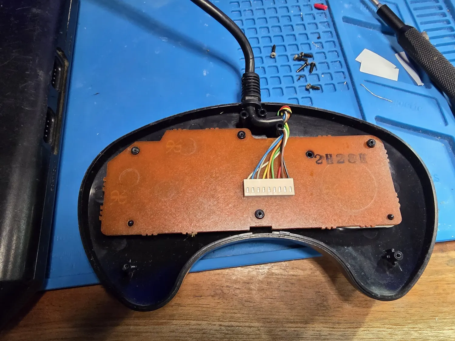
The multiplexer approach is unusual enough to be worth seeing side by side with the Nintendo shift-register pads: Controllers: How Five Consoles Read a Button does that.
I have the 3-button internals from my own bench rather than from a Sega schematic, so there is no pin-by-pin table for the pad here: the port pinout below is OEM-sourced and is the part you actually need for a cable repair or an adapter build.
Chip and connector pinouts
The component library: each IC and connector defined once, with the revision badge on the card showing which boards it sits on. The Sega custom gate arrays and the VDP have no public datasheet, so those cards are deliberately empty. The ones that do have full pin tables are the parts I could read off a datasheet or an OEM schematic sheet.
Two cards are worth opening before anything else. The 68000 appears twice, because the DIP-64 on the early Model 1 boards and the PLCC-68 on VA7 and every Model 2 are different pin maps and carrying numbers across them will waste an afternoon. And the two DC jacks are separate cards for the same reason the polarity warning is at the top of this page.
Components & pinouts
Each part is defined once. The revision badge on every card shows exactly which board revision(s) it applies to.
Every diagram rotates and flips to match the board in front of you, zooms from a whole-package overview up to 3.2×, and saves at the orientation you are looking at — ↓ SVG matches the screen, and ↓ SVG (print) gives you the same drawing as ink on white. Both are vector, so print them at any size you like, which is the better route for the long connector pinouts since printing this page has to shrink them to fit the sheet. The # beside a part name links to that card, and the one in the pin panel links to a single pin — either link opens the card for whoever you send it to.
Audio amplifier (Sega-branded ROHM) Sega 315-5684 (ROHM BA6166FS) M2-VA2 · M2-VA2.3 · M2-VA3 · M2-VA4 sopsingle sourcecm-mb,c5-m2,cm-aud#
IC9 (IC4 on VA4): the amp fitted alongside the discrete-YM2612 Model 2 boards and the short boards. No public datasheet, so the pin table is empty.
Sources identify this as a rebadged ROHM BA6166FS, and Console5’s own page for the part calls it a sound network / headphone amp. That is the whole of the public record. ROHM no longer publish the BA6166 family and none of the aggregators hold it.
Searched again 2026-08-11 in a browser rather than with curl, since a JavaScript viewer is the usual reason a document looks absent when it is not. BA6166 and BA6166FS return nothing on datasheet4u and nothing on datasheetarchive, and alldatasheet has no entry: its index runs BA6162 straight to BA6191. The Datasheet Archive’s own ROHM part index does the same. Console5 has a wiki page for BA6166FS, but it carries no PDF and no pin diagram.
That page does settle one thing: Console5 title it Sega 315-5864 / Rohm BA6166FS, where their Model 2 IC list (the source for the part number at the top of this card) prints 315-5684. Their wiki redirects both spellings to the same page, so one of the two is a transposition on their side. Read the marking on your own board.
No pins captured yet — bench stub.
Headphone preamp / amplifier Sony CXA1034P (early boards: HA1034 or Matsushita AN7108) M1-VA0 · M1-VA1 · M1-VA2 · M1-VA3 · M1-VA4 · M1-VA5 · M1-VA6 · M1-VA6.5 · M1-VA6.8 dip-16single sourcec5-cxa1034,ds4u-cxa1034-redraw,c5-m1,rs-hw,cm-mb#
IC12 on the IC-series boards: this is the part behind the 'early Model 1 sounds louder' story, not the FM chip
No pin map. There is no public Sony datasheet for the CXA1034P: Console5’s own page for the part says flatly that they were unable to find one, and that its pinout only “suggests similarity” to the CXA1634P/M and the AN7108. That is a resemblance, not a source, so those parts are not folded into one pin table here.
What the aggregators carry, and what it is good for. They hold a
single-page redrawn application circuit, attributed to no manufacturer and
watermarked by the host. I have archived it anyway
(datasheet4u-cxa1034p-redrawn-appcircuit-p1.png) because it settles the
package and the headline electricals even though it cannot carry a pin
map: DIP-16 for the P suffix and SO-16 for the M, Vcc 1.8-7.5 V,
2 x 0.03 W into 32 ohm, 65 dB gain. The 16-pin figure below rests on that
drawing and wants a leg-count on a real board to become bench-confirmed.
What matters here anyway is attribution. The often-repeated claim that VA0 through VA2 “sound better” is, per ConsoleMods, a slightly overdriven headphone preamp: louder, but it distorts on some games. VA3 corrected the overdrive and added a gentle low-pass, and that is the combination people actually mean when they call VA3 the audio baseline. On my bench I treat this as a circuit-character difference, not a fault to chase.
Only Model 1 has this path at all: the front headphone jack is Model 1 only, and it is where the stereo lives, since the 8-pin DIN carries mono.
Click a pin to see its signal, net, and sources.
Interactive diagram needs JavaScript. The full pinout is in the table below.
No pins captured yet — bench stub.
FC1004 ASIC (VDP + I/O + YM3438) Sega 315-5487 / -5487-01 / -5487-10 (Yamaha FC1004) M1-VA7 · M2-VA0 qfp✓cm-mb,cm-aud,c5-m1,c5-m2#
IC6 on VA7: VDP, I/O and a modified YM3438 FM core on one die; this is the part with the broken 50 Hz mode
No datasheet. The FC1004 is the single change that makes VA7 “basically a Model 2 PCB in a Model 1 case”, as Console5 puts it: it takes the VDP, the I/O controller and the FM synth onto one die, which is why VA7 has no discrete YM2612 and only one 7805.
The 50 Hz problem is the practical consequence and it matters for resale: the 315-5487 does not implement 50 Hz properly (games lose sound or crash), and the Japanese 315-5487-10 has no 50 Hz mode at all. Do not sell a 50/60 Hz switch on a 315-5487 board. Some Brazilian VA7 boards use the revised 315-5660 instead, which does run both cleanly. Jailbar work on this family taps the subcarrier at pin 131 rather than the 315-5313’s pin 50.
No pins captured yet — bench stub.
FC1004-family ASIC (revised) Sega 315-5660 / -5660-02 (also 315-5700, 315-5708 Fujitsu on some boards) M2-VA0 · M2-VA1 · M2-VA1.8 · M2-VA3 qfp✓cm-mb,c5-m2,cm-bg#
IC6 on most Model 2: same FC1004 lineage as the 315-5487 with the 50 Hz mode fixed; still carries the YM3438 FM core, so no discrete YM2612
No pins captured yet — bench stub.
Model 2 ASIC without an FM core (flawed VDP) Sega 315-5685 M2-VA2.3 qfp✓cm-mb,c5-m2,cm-bg#
the late VA2.3 part with a broken VDP: shadow/highlight mode is wrong and rasters glitch; MK-1631A on the label usually means this chip
No datasheet. This is a genuine defect, not a preference: shadow and highlight rendering is broken and raster effects glitch on games that use them. Multiple wikis agree, and it is the single strongest reason to check a Model 2’s model number before buying one to restore. It cannot be fixed in software or by recapping: the only cure is a different board.
Subcarrier for jailbar work is pin 103, same as the 315-5786.
No pins captured yet — bench stub.
Model 2 ASIC without an FM core (good revision) Sega 315-5786 (Toshiba) M2-VA2 · M2-VA2.3 qfp✓cm-mb,c5-m2,cm-bg#
IC6 on VA2 and early VA2.3: no YM3438 core, which is why these boards go back to a discrete YM2612; the good half of the VA2.3 lottery
No datasheet. Two things follow from the missing FM core. First, VA2 and VA2.3 fit a real YM2612 again, which is why they are interesting to people chasing early-Model-1 FM character on a Model 2 shell. Second, ConsoleMods and Console5 both report the FM is mixed too loud against the PSG on VA2.
On VA2.3 this part is the one you want: a plain MK-1631 model number implies the 315-5786, while MK-1631A implies the flawed 315-5685. Both wikis note that is a strong tendency, not an absolute: read the die. Subcarrier for jailbar work is pin 103 on this family.
No pins captured yet — bench stub.
GOAC: whole console on one die Sega 315-5960 (Yamaha FJ3002) M2-VA4 qfpsingle sourcecm-mb,c5-m2#
IC1 on the Model 2 VA4 short board: 68000, Z80, VDP, YM3438, I/O and Z80 RAM all on one die; only RAM, VRAM, encoder and amp remain outside
No pins captured yet — bench stub.
GOAC (Genesis 3) Sega 315-6123 (Yamaha FQ8007) M3 qfpsingle sourcecm-mb,cm-bg#
Genesis 3 only: a different GOAC that also merges main and video RAM into a single 128 KB SDRAM
No pins captured yet — bench stub.
A/V out: Model 1 (8-pin DIN) Full-size 8-pin DIN, 270 degree: the same connector and pinout as the Master System M1-VA0 · M1-VA1 · M1-VA2 · M1-VA3 · M1-VA4 · M1-VA5 · M1-VA6 · M1-VA6.5 · M1-VA6.8 · M1-VA7 din-8-8single sourcecm-pin,pg1,rs-av1,oem-m1av#
the pin NUMBERING on this connector is genuinely contested across three sources: the signal set is agreed, the numbers are not, so buzz it out before wiring a cable
This is the half of the Model 1 versus Model 2 A/V split that catches people, and it is the one place on this page where I will not give you a clean answer. The signal set is agreed everywhere: composite video, ground, mono audio, green, +5 V, composite sync, blue and red are all present. The pin numbers are not agreed.
Three sources, three answers:
- ConsoleMods: 1 composite, 2 GND, 3 audio, 4 green, 5 +5 V, 6 sync, 7 blue, 8 red.
- PinoutGuide (independent): the same 1 through 6, but 7 red and 8 blue, the opposite of ConsoleMods on the last two. That page also self-flags uncertainty about whether 1 and 3 are swapped.
- The OEM Model 1 Sound and Video schematic sheet, read at high zoom: 1 audio, 2 GND, 3 video, 4 +5 V, 5 green, 6 red, 7 C-sync, 8 blue. An entirely different numbering.
The OEM sheet is not obviously wrong: the same-vintage OEM Model 2 sheet’s pin numbers do match the community Model 2 numbering, so the OEM appears to be using true physical pin numbers and the Model 1 divergence is real, not a drafting quirk. I have listed the ConsoleMods numbering below because it is the one most cables are built to, and tagged the whole thing single-source. Meter continuity on the actual board before you commit an RGB cable to it.
Two other things about this connector. It carries mono audio only: on Model 1 the stereo lives on the front headphone jack. And it supplies +5 V, which is how active SCART and RGB amps in the cable get powered, so a shorted cable can pull the console’s rail down. “Boots without the cable, dies with it” points straight here.
It is a non-standard Sega footprint, so no distributor stocks a drop-in. Failures are nearly always cold or cracked joints: reflow first, and replace only with a salvage socket or a specialty repro.
| Pin | Signal | Cat | Net | Note |
|---|---|---|---|---|
| 1 | Composite video | signal | cvbs | unused on the French Model 1, which is RGB-only single source |
| 2 | GND | gnd | gnd | single source |
| 3 | Audio (mono) | signal | audio | mono only: Model 1 stereo is on the front headphone jack single source |
| 4 | Green | signal | rgb_g | single source |
| 5 | +5V | rail | v5 | powers an active RGB/SCART cable; a shorted cable drags the console rail down single source |
| 6 | Composite sync | signal | csync | single source |
| 7 | Blue | signal | rgb_b | CONTESTED: PinoutGuide gives red here, and the OEM sheet gives C-sync; buzz it out single source |
| 8 | Red | signal | rgb_r | CONTESTED: PinoutGuide gives blue here, and the OEM sheet gives blue too; buzz it out single source |
A/V out: Model 2 and 3 (9-pin mini-DIN) 9-pin mini-DIN: shared with the Nomad, Mega Jet, 32X, CDX, Aiwa Mega CD and most X'Eye M2-VA0 · M2-VA1 · M2-VA1.8 · M2-VA2 · M2-VA2.3 · M2-VA3 · M2-VA4 · M3 mini-din-9-9✓cm-pin,pg2,oem-m2av#
the counterpart to the Model 1 DIN and the reason Model 2 has stereo on the A/V port and no headphone jack; ground is the cable shroud, not a pin
Unlike the Model 1 connector, this one is settled: ConsoleMods, PinoutGuide and the OEM Model 2 service schematic all agree, so it is genuinely two-plus-source verified. Ground is the shell.
This is where the Model 2 gains and loses against the Model 1. It gains stereo on the A/V port itself (pins 8 and 9), and loses the front headphone jack entirely. On the Genesis 3 the connector is physically the same and carries the stereo pins, but the console outputs mono duplicated onto the left channel: not a contradiction, just a different console behind the same socket.
Same +5 V caveat as the Model 1 port: pin 2 powers active cables, and a shorted cable can pull the rail down. Also a non-standard Sega footprint with no distributor drop-in; reflow before replacing.
| Pin | Signal | Cat | Net | Note |
|---|---|---|---|---|
| 1 | Blue | signal | rgb_b | ✓ |
| 2 | +5V | rail | v5 | powers an active RGB/SCART cable ✓ |
| 3 | Green | signal | rgb_g | ✓ |
| 4 | Composite video | signal | cvbs | ✓ |
| 5 | Composite sync | signal | csync | ✓ |
| 6 | Mono audio | signal | audio | ✓ |
| 7 | Red | signal | rgb_r | ✓ |
| 8 | Left audio | signal | audio_l | carries mono on the Genesis 3 ✓ |
| 9 | Right audio | signal | audio_r | unused on the Genesis 3 ✓ |
| shell | GND | gnd | gnd | ground is the connector shroud, not a numbered pin: listed here so it is not forgotten ✓ |
Cartridge slot (2 x 32 card edge) 64-pin card edge: row A rear, row B front, each numbered left to right with the port facing left M1-VA0 · M1-VA1 · M1-VA2 · M1-VA3 · M1-VA4 · M1-VA5 · M1-VA6 · M1-VA6.5 · M1-VA6.8 · M1-VA7 · M2-VA0 · M2-VA1 · M2-VA1.8 · M2-VA2 · M2-VA2.3 · M2-VA3 · M2-VA4 card-edge-64single sourcecm-pin#
the raw 68000 bus on an edge connector: the best place on the console to probe address, data, clock and reset without unshielding anything
Transcribed from ConsoleMods’ connector-pinout page, which is the deepest published table; it is one source, so treat it as such. The “V” prefix on the signal names means the line runs to the 68000. Pin numbering here is not sequential 1–64: it is two rows of 32, A1–A32 on the rear and B1–B32 on the front, so the numbers below are given as row+position and there is no drawn diagram for this connector.
The probe points I actually use: B19 VCLK for a live 68000 clock without opening the shield, A2/A31 for the +5 V rail at the slot, B2 MRES for system reset, B27 VRES for the 68000’s own reset, B18 AS and B20 DTACK for bus activity. Dirty or worn edge contacts are a top failure mode on these and give garbled graphics, crashes or a dead slot: clean and burnish before condemning anything.
B1 and B3 (SL1/SR1) are external audio in from the 32X per ConsoleMods; GameSX marks the same pins unknown, so that one is flagged single-source. The “unused on Genesis 3” annotations are why the Genesis 3 breaks the 32X, Sega CD passthrough and Virtua Racing.
| Pin | Signal | Cat | Net | Note |
|---|---|---|---|---|
| A1 | GND | gnd | gnd | bridge-ok single source |
| A2 | +5V | rail | v5 | rail at the slot bridge-ok single source |
| A3 | VA8 | bus | abus | single source |
| A4 | VA11 | bus | abus | single source |
| A5 | VA7 | bus | abus | single source |
| A6 | VA12 | bus | abus | single source |
| A7 | VA6 | bus | abus | single source |
| A8 | VA13 | bus | abus | single source |
| A9 | VA5 | bus | abus | single source |
| A10 | VA14 | bus | abus | single source |
| A11 | VA4 | bus | abus | single source |
| A12 | VA15 | bus | abus | single source |
| A13 | VA3 | bus | abus | single source |
| A14 | VA16 | bus | abus | single source |
| A15 | VA2 | bus | abus | single source |
| A16 | VA17 | bus | abus | single source |
| A17 | VA1 | bus | abus | lowest address line: the 68000 has no A0 single source |
| A18 | GND | gnd | gnd | bridge-ok single source |
| A19 | VD7 | bus | dbus | single source |
| A20 | VD0 | bus | dbus | single source |
| A21 | VD8 | bus | dbus | single source |
| A22 | VD6 | bus | dbus | single source |
| A23 | VD1 | bus | dbus | single source |
| A24 | VD9 | bus | dbus | single source |
| A25 | VD5 | bus | dbus | single source |
| A26 | VD2 | bus | dbus | single source |
| A27 | VD10 | bus | dbus | single source |
| A28 | VD4 | bus | dbus | single source |
| A29 | VD3 | bus | dbus | single source |
| A30 | VD11 | bus | dbus | single source |
| A31 | +5V | rail | v5 | bridge-ok single source |
| A32 | GND | gnd | gnd | bridge-ok single source |
| B1 | SL1 | signal | sl1 | external left audio in (32X); GameSX marks this pin unknown, so it is single-sourced single source |
| B2 | MRES | signal | mres | system reset: the RC-timed master reset, see the schematic facts single source |
| B3 | SR1 | signal | sr1 | external right audio in (32X); same single-source caveat as B1 single source |
| B4 | VA9 | bus | abus | single source |
| B5 | VA10 | bus | abus | single source |
| B6 | VA18 | bus | abus | single source |
| B7 | VA19 | bus | abus | single source |
| B8 | VA20 | bus | abus | single source |
| B9 | VA21 | bus | abus | single source |
| B10 | VA22 | bus | abus | single source |
| B11 | VA23 | bus | abus | single source |
| B12 | YS | signal | ys | blanking single source |
| B13 | VSYNC | signal | vsync | vertical sync out to the cart single source |
| B14 | HSYNC | signal | hsync | horizontal sync out to the cart single source |
| B15 | EDCLK | signal | edclk | external dot clock: the H40-mode clock the early boards had to synthesise single source |
| B16 | CAS0 | signal | cas0 | single source |
| B17 | CE_0 | signal | ce0 | cartridge chip enable single source |
| B18 | AS | signal | as | 68000 address strobe: good bus-activity probe single source |
| B19 | VCLK | signal | vclk | 68000 clock, ~7.67 MHz NTSC / 7.60 MHz PAL: the healthy-clock probe point without opening the shield single source |
| B20 | DTACK | signal | dtack | data transfer acknowledge single source |
| B21 | CAS2 | signal | cas2 | single source |
| B22 | VD15 | bus | dbus | single source |
| B23 | VD14 | bus | dbus | single source |
| B24 | VD13 | bus | dbus | single source |
| B25 | VD12 | bus | dbus | single source |
| B26 | ASEL | signal | asel | the line the Model 2 VA2 bodge board fixes with a 74HC14 for Virtua Racing and the 32X single source |
| B27 | VRES | signal | vres | 68000 reset single source |
| B28 | LWR | signal | lwr | lower byte write enable single source |
| B29 | UWR | signal | uwr | upper byte write enable single source |
| B30 | M3 | signal | m3 | Master System mode enable: what the Power Base Converter asserts single source |
| B31 | TIME | signal | time | single source |
| B32 | CART | signal | cart | cartridge enable single source |
Controller port (female DE-9) DE-9 female, 3-button and 6-button compatible M1-VA0 · M1-VA1 · M1-VA2 · M1-VA3 · M1-VA4 · M1-VA5 · M1-VA6 · M1-VA6.5 · M1-VA6.8 · M1-VA7 · M2-VA0 · M2-VA1 · M2-VA1.8 · M2-VA2 · M2-VA2.3 · M2-VA3 · M2-VA4 · M3 de-9-9✓cm-pin,rs-ctrl#
pin 7 SELECT multiplexes which buttons appear on the data pins, and scoping it tells you whether a game is running even with no picture
Two independent sources agree on this one: ConsoleMods for the button and direction multiplex, RetroSix for the SELECT-drive protocol. The pin numbering below is the connector at the console.
How it works: the console drives SELECT (pin 7) high or low, and the same data pins report a different button set in each state. A 6-button pad detects rapid SELECT toggling (under 12 ms between edges) and on the third low pulse returns all four directions low as an ID handshake, then exposes X, Y, Z and Mode on the next high. Everything idles high on pull-ups until a game starts polling.
The trick I actually use: scope pin 7. It sits idle-high during the SEGA logo and starts pulsing once the game is running: Sonic pulses low every 20 ms or so, Mortal Kombat II does the inverse. Pulses with a black screen means the CPU and cart are fine and the fault is in the video chain.
Most “dead controller port” faults are cracked solder joints, so reflow before replacing. A generic right-angle DE-9 is electrically correct but the mounting footprint differs from Sega’s: dry-fit or pull a salvage port.
| Pin | Signal | Cat | Net | Note |
|---|---|---|---|---|
| 1 | Up / Z | signal | d0 | Up; button Z on the 6-button extra read ✓ |
| 2 | Down / Y | signal | d1 | Down; button Y on the extra read ✓ |
| 3 | Left / GND / X | signal | d2 | Left with SELECT high, pulled to ground with SELECT low; button X on the extra read ✓ |
| 4 | Right / GND / Mode | signal | d3 | Right with SELECT high, grounded with SELECT low; Mode on the extra read ✓ |
| 5 | +5V | rail | v5 | controller supply: a shorted pad or cable can drag the console rail down ✓ |
| 6 | B / A | signal | d4 | button B with SELECT high, button A with SELECT low ✓ |
| 7 | SELECT | signal | select | console output, game-driven: the pin to scope to prove a game is running ✓ |
| 8 | GND | gnd | gnd | ✓ |
| 9 | C / Start | signal | d5 | button C with SELECT high, Start with SELECT low ✓ |
Expansion port: Sega CD (2 x 30 card edge) 60-pin card edge: row A bottom, row B top, each numbered left to right with the port facing left M1-VA0 · M1-VA1 · M1-VA2 · M1-VA3 · M1-VA4 · M1-VA5 · M1-VA6 · M1-VA6.5 · M1-VA6.8 · M1-VA7 · M2-VA0 · M2-VA1 · M2-VA1.8 · M2-VA2 · M2-VA2.3 · M2-VA3 · M2-VA4 card-edge-60single sourcecm-pin#
a second copy of the 68000 bus plus the Sega CD control lines and the four audio-mix pins: present on all Model 1 and Model 2, gone on the Genesis 3
ConsoleMods again, single-sourced. Note this is a different connector from the rear EXT serial port, which trips people up: the expansion port is the side edge the Sega CD docks into, and every Model 1 and Model 2 has one.
For a Sega CD no-audio fault, the four audio-mix pins are the first check: SL3/SR3 (B27/A27) carry Genesis audio out to the CD, and SL2/SR2 (B29/A29) carry CD and expansion audio back in. Pin numbering is row plus position, not sequential 1 to 60, so there is no drawn diagram.
| Pin | Signal | Cat | Net | Note |
|---|---|---|---|---|
| A1 | GND | gnd | gnd | bridge-ok single source |
| A2 | VA19 | bus | abus | single source |
| A3 | CAS0 | signal | cas0 | single source |
| A4 | VD0 | bus | dbus | single source |
| A5 | VD1 | bus | dbus | single source |
| A6 | VD2 | bus | dbus | single source |
| A7 | VD3 | bus | dbus | single source |
| A8 | VD4 | bus | dbus | single source |
| A9 | VD5 | bus | dbus | single source |
| A10 | VD6 | bus | dbus | single source |
| A11 | VD7 | bus | dbus | single source |
| A12 | GND | gnd | gnd | bridge-ok single source |
| A13 | VD8 | bus | dbus | single source |
| A14 | VD9 | bus | dbus | single source |
| A15 | VD10 | bus | dbus | single source |
| A16 | VD11 | bus | dbus | single source |
| A17 | VD12 | bus | dbus | single source |
| A18 | VD13 | bus | dbus | single source |
| A19 | VD14 | bus | dbus | single source |
| A20 | VD15 | bus | dbus | single source |
| A21 | ROM | signal | rom | single source |
| A22 | ASEL | signal | asel | single source |
| A23 | RAS2 | signal | ras2 | single source |
| A24 | FDC | signal | fdc | Sega CD control line single source |
| A25 | FRES | signal | fres | Sega CD reset single source |
| A26 | +5V | rail | v5 | bridge-ok single source |
| A27 | SR3 | signal | sr3 | Genesis right audio OUT to the CD: first check on a Sega CD no-audio fault single source |
| A28 | +5V In | rail | v5in | bridge-ok single source |
| A29 | SR2 | signal | sr2 | expansion right audio IN from the CD single source |
| A30 | GND | gnd | gnd | bridge-ok single source |
| B1 | GND | gnd | gnd | bridge-ok single source |
| B2 | DISK | signal | disk | Sega CD control line single source |
| B3 | VA1 | bus | abus | single source |
| B4 | VA2 | bus | abus | single source |
| B5 | VA3 | bus | abus | single source |
| B6 | VA4 | bus | abus | single source |
| B7 | VA5 | bus | abus | single source |
| B8 | VA6 | bus | abus | single source |
| B9 | VA7 | bus | abus | single source |
| B10 | VA8 | bus | abus | single source |
| B11 | VA9 | bus | abus | single source |
| B12 | GND | gnd | gnd | bridge-ok single source |
| B13 | VA10 | bus | abus | single source |
| B14 | VA11 | bus | abus | single source |
| B15 | VA12 | bus | abus | single source |
| B16 | VA13 | bus | abus | single source |
| B17 | VA14 | bus | abus | single source |
| B18 | VA15 | bus | abus | single source |
| B19 | VA16 | bus | abus | single source |
| B20 | VA17 | bus | abus | single source |
| B21 | LWR | signal | lwr | single source |
| B22 | UWR | signal | uwr | single source |
| B23 | CAS2 | signal | cas2 | single source |
| B24 | FDWR | signal | fdwr | Sega CD control line single source |
| B25 | VA18 | bus | abus | single source |
| B26 | +5V | rail | v5 | bridge-ok single source |
| B27 | SL3 | signal | sl3 | Genesis left audio OUT to the CD single source |
| B28 | +5V In | rail | v5in | bridge-ok single source |
| B29 | SL2 | signal | sl2 | expansion left audio IN from the CD single source |
| B30 | GND | gnd | gnd | bridge-ok single source |
EXT serial port (female DE-9) DE-9 female: electrically a controller port with serial TX/RX overloaded on pins 6 and 9 M1-VA0 · M1-VA1 · M1-VA2 · M1-VA3 · M1-VA4 · M1-VA5 · M1-VA6 de-9-9single sourcecm-pin,cm-mb#
presence is a revision tell in itself: fitted through VA6 in most markets and on every Japanese Mega Drive, deleted from VA6.5 onward
ConsoleMods is the only pinout source I have for this port, so it is single-sourced. It is electrically identical to a controller port and does VDP serial I/O; the only notable accessory that used it was the Japan-only Mega Modem. Levels are 5 V TTL, not RS-232: do not hang a real serial cable on it without level shifting.
Its real value on the bench is identification. VA6.5 is literally a VA6 with this port and the line filters deleted, so a blanked-off rear EXT cutout with the other ports in their original positions is a strong VA6.5 tell. Japanese Model 1 boards keep it later than other markets, which is also why Japanese units moved the power jack to a small satellite PCB.
| Pin | Signal | Cat | Net | Note |
|---|---|---|---|---|
| 1 | Up | signal | d0 | single source |
| 2 | Down | signal | d1 | single source |
| 3 | Left / GND | signal | d2 | single source |
| 4 | Right / GND | signal | d3 | single source |
| 5 | +5V | rail | v5 | single source |
| 6 | B / A / TX | signal | d4 | transmit in serial mode, 5 V TTL single source |
| 7 | SELECT | signal | select | single source |
| 8 | GND | gnd | gnd | single source |
| 9 | C / Start / RX | signal | d5 | receive in serial mode, 5 V TTL single source |
RGB-to-composite video encoder Sony CXA1145P (DIP, Model 1) / CXA1145M (SMD, VA7 and Model 2) M1-VA0 · M1-VA1 · M1-VA2 · M1-VA3 · M1-VA4 · M1-VA5 · M1-VA6 · M1-VA6.5 · M1-VA7 · M2-VA0 · M2-VA1 · M2-VA1.8 · M2-VA3 dip-24✓ds-cxa1145,sch-va4av,rs-cxa,c5-m1,c5-m2#
IC13 on the IC-series boards, IC11 on VA7 and Model 2, and the chip that quietly supplies the reset comparator's reference voltage
Pin map read off the Sony CXA1145P/M datasheet: the block-diagram pin configuration on sheet 2, checked pin by pin against the four sheets of per-pin descriptions that follow it. The P is the 24-pin DIP and the M is the 24-pin SOP, and Sony documents both under one pin table, so these numbers hold for either package. The diagram drawn here is the DIP.
Pin 14 is the one that links two subsystems that look unrelated: the reset supervisor’s comparator takes its reference from the encoder’s VREF pin. A sick encoder can therefore hold a Model 1 in reset: powers up, 5 V present, never boots. That routing is from the VA4 A/V schematic sheet, not from Sony; the datasheet only says VREF is the internal reference voltage and wants roughly 10µF to ground on it.
Two things the datasheet settles that matter on the bench. The chroma and luma paths leave and re-enter the chip (pin 15 out through a band-pass filter into pin 17, pin 16 out through a delay line into pin 18), so a dead composite output alongside healthy RGB is worth chasing at those external parts before condemning the encoder. And pin 7 is a hard mode strap: Vcc selects NTSC, ground selects PAL.
Function-wise it takes analog RGB plus composite sync from the VDP and produces composite video plus buffered RGB and sync out to the AV port. It also amplifies the incoming RGB by roughly 40 percent, so levels measured at the connector are encoder-buffered, not raw VDP levels.
Later boards substitute other encoders and composite quality varies with them even where the digital side is identical: Sony CXA1645 (better), Samsung KA2195D (blurrier), Fujitsu MB3514, ROHM BH7236AF on 1998 PAL units. On the French Model 1 (1600-09 / 1601-09) there is no composite at all (RGB only), so an RGB cable that pulls sync from composite will not work on one.
Click a pin to see its signal, net, and sources.
Interactive diagram needs JavaScript. The full pinout is in the table below.
| Pin | Signal | Cat | Net | Note |
|---|---|---|---|---|
| 1 | GND1 | gnd | gnd | ground for everything except the RGB and composite output drivers bridge-ok ✓ |
| 2 | R IN | signal | rin | analog R from the VDP, 100% = 1 Vp-p ✓ |
| 3 | G IN | signal | gin | analog G from the VDP, 100% = 1 Vp-p ✓ |
| 4 | B IN | signal | bin | analog B from the VDP, 100% = 1 Vp-p ✓ |
| 5 | XO OUT | signal | xo | subcarrier oscillator output: crystal across pins 5 and 6 for internal oscillation ✓ |
| 6 | XO IN | signal | xo | subcarrier oscillator input; external subcarrier is coupled in here at 400–1000 mVp-p ✓ |
| 7 | NTSC/PAL | signal | mode | mode strap: Vcc = NTSC, GND = PAL ✓ |
| 8 | AUDIO IN | signal | audin | audio buffer input, about 25 kΩ ✓ |
| 9 | AUDIO OUT | signal | audout | audio buffer output ✓ |
| 10 | C SYNC IN | signal | csyncin | composite sync from the VDP, TTL levels, low = sync ✓ |
| 11 | C SYNC OUT | signal | csyncout | buffered composite sync, drives 75Ω directly ✓ |
| 12 | Vcc1 | rail | vcc1 | +5V for everything except the RGB and composite output drivers ✓ |
| 13 | IREF | signal | iref | internal reference current: 27 kΩ to ground ✓ |
| 14 | VREF | rail | vref | internal reference voltage, 10µF to ground; on Model 1 this node also feeds the reset comparator: read on the VA4 PAL-G A/V sheet ✓ |
| 15 | C OUT | signal | cout | chroma out: goes off-chip through a band-pass filter and back in at pin 17 ✓ |
| 16 | Y OUT | signal | yout | luma out: goes off-chip through a delay line and back in at pin 18 ✓ |
| 17 | C IN | signal | cin | chroma back in after the band-pass filter ✓ |
| 18 | Y IN | signal | yin | luma back in after the delay line ✓ |
| 19 | Vcc2 | rail | vcc2 | +5V for the RGB and composite output drivers: Sony calls for a large decoupling cap here because the current is heavy ✓ |
| 20 | CV OUT | signal | cvout | composite video out of the Y/C mix, drives 75Ω directly ✓ |
| 21 | B OUT | signal | bout | buffered analog B, 75Ω drive ✓ |
| 22 | G OUT | signal | gout | buffered analog G, 75Ω drive ✓ |
| 23 | R OUT | signal | rout | buffered analog R, 75Ω drive ✓ |
| 24 | GND2 | gnd | gnd | ground for the RGB and composite output drivers bridge-ok ✓ |
RGB-to-composite video encoder (improved Sony) Sony CXA1645M M2-VA2.3 · M2-VA3 · M2-VA4 sop-24✓ds-cxa1645,c5-m2,cm-mb#
IC11/IC5 on later Model 2: the better-looking composite encoder of the family
Pin map read off the Sony CXA1645P/M datasheet (document E93411A41-ST): the block-diagram pin configuration on sheet 1, checked against the per-pin description tables on sheets 2 through 5. The P is the 24-pin DIP and the M is the 24-pin SOP under one pin table; Model 2 fits the M.
Do NOT assume it is a drop-in for a CXA1145. Seventeen of the twenty-four pins do land on the same signal, which is why it looks like one, but seven do not and several of those matter. The 1645 has no crystal oscillator: a subcarrier has to be fed in at pin 6, where the 1145 drives a crystal from 5 and 6. It has no audio buffer at all: pins 8 and 9, which are the 1145’s AUDIO IN and AUDIO OUT, are a burst-flag monitor and a Y-clamp time constant here. It has no composite-sync output; pin 11 is a no-connect. Pins 17 and 18, the 1145’s chroma and luma return legs, are a subcarrier trap and a filter-fo trim resistor. And pin 13 wants 47 kΩ where the 1145 wants 27 kΩ.
Sources describe it as a visible step up from the CXA1145 on composite, and the datasheet backs the mechanism: the band-pass filter for chroma and the delay line for luma are on-chip here instead of being external parts Sega had to buy, lay out and let age. 1998 PAL VA4 boards use a ROHM BH7236AF instead, which I have not been able to source a datasheet for.
Click a pin to see its signal, net, and sources.
Interactive diagram needs JavaScript. The full pinout is in the table below.
| Pin | Signal | Cat | Net | Note |
|---|---|---|---|---|
| 1 | GND1 | gnd | gnd | ground for everything except the RGB, composite and Y/C output drivers bridge-ok ✓ |
| 2 | RIN | signal | rin | analog R in, 100% = 1 Vp-p max ✓ |
| 3 | GIN | signal | gin | analog G in, 100% = 1 Vp-p max ✓ |
| 4 | BIN | signal | bin | analog B in, 100% = 1 Vp-p max ✓ |
| 5 | NC | nc | no connection ✓ | |
| 6 | SCIN | signal | fsc | subcarrier in, 0.4–0.5 Vp-p, sine or pulse: no on-chip crystal oscillator on this part ✓ |
| 7 | NPIN | signal | mode | mode strap: Vcc = NTSC, GND = PAL ✓ |
| 8 | BFOUT | signal | bfout | burst-flag pulse monitor out; will not drive 75Ω ✓ |
| 9 | YCLPC | signal | yclpc | Y clamp time constant: 0.1µF to ground ✓ |
| 10 | SYNC IN | signal | csyncin | composite sync in, TTL levels, low = sync period ✓ |
| 11 | NC | nc | no connection ✓ | |
| 12 | VCC1 | rail | vcc1 | +5V for everything except the output drivers ✓ |
| 13 | IREF | signal | iref | internal reference current: 47 kΩ to ground (the CXA1145 wants 27 kΩ, so this is not a like-for-like part swap) ✓ |
| 14 | VREF | rail | vref | internal reference voltage, roughly 10µF decoupling ✓ |
| 15 | COUT | signal | cout | chroma out, 75Ω drive ✓ |
| 16 | YOUT | signal | yout | luma out, 75Ω drive ✓ |
| 17 | YTRAP | signal | ytrap | subcarrier trap for the composite output: cap, or cap and inductor in series, to ground; does not affect YOUT ✓ |
| 18 | FO | signal | fo | internal filter fo trim: 20 kΩ ±1% for NTSC, 16 kΩ ±1% for PAL ✓ |
| 19 | VCC2 | rail | vcc2 | +5V for the RGB, composite and Y/C output drivers: 10µF or more here ✓ |
| 20 | CVOUT | signal | cvout | composite video out, 75Ω drive ✓ |
| 21 | BOUT | signal | bout | buffered analog B, 75Ω drive ✓ |
| 22 | GOUT | signal | gout | buffered analog G, 75Ω drive ✓ |
| 23 | ROUT | signal | rout | buffered analog R, 75Ω drive ✓ |
| 24 | GND2 | gnd | gnd | ground for the RGB, composite and Y/C output drivers bridge-ok ✓ |
RGB-to-composite video encoder (Fujitsu) Fujitsu MB3514 / MB3514PF (SMD) M1-VA6.8 · M2-VA0 · M2-VA1 · M2-VA1.8 sop-24✓ds-mb3514,cm-mb,c5-m2,rs-caps2#
the SMD encoder that replaces the DIP CXA1145P on the PAL-only VA6.8, and appears on many PAL Model 2 boards
Pin map read off Fujitsu data sheet DS04-28020-1E. The pin-assignment drawing and the per-pin description table. 24-pin plastic SOP, package FPT-24P-M01.
Reading the Fujitsu and the Sony sheets side by side explains why Sega could swap these parts around without re-laying the board: the MB3514 sits pin-for-pin on top of the CXA1145 at twenty-one of twenty-four pins, mode strap included. High is NTSC and low is PAL on both. Three pins genuinely differ. Pin 5 is a 100 pF phase-generating cap here where the Sony has its subcarrier oscillator output. Pin 11 is a no-connect here where the Sony has buffered composite sync out, so a board built around an MB3514 cannot hand you CSYNC from the encoder at all. Pin 13 is a no-connect here where the Sony wants its IREF resistor. Pin 6 is subcarrier-in on both, just named differently.
Its practical importance is still mostly in the cap order: on Model 2 VA0/VA1/VA1.8, CE14 is 220µF/6.3V on an MB3514 board but 10µF/16V on a CXA1145 or KA2195D board. Read the encoder before ordering a kit.
Click a pin to see its signal, net, and sources.
Interactive diagram needs JavaScript. The full pinout is in the table below.
| Pin | Signal | Cat | Net | Note |
|---|---|---|---|---|
| 1 | GND1 | gnd | gnd | ground for everything except the 75Ω output drivers bridge-ok ✓ |
| 2 | R-IN | signal | rin | analog R in, 100% = 1 Vp-p; clamped while CSYNC-IN is low ✓ |
| 3 | G-IN | signal | gin | analog G in, 100% = 1 Vp-p ✓ |
| 4 | B-IN | signal | bin | analog B in, 100% = 1 Vp-p ✓ |
| 5 | C | signal | phasec | phase-generating capacitor: 100 pF to ground ✓ |
| 6 | fsc-IN | signal | fsc | subcarrier in through a coupling cap, 300–700 mVp-p ✓ |
| 7 | NTSC/PAL-IN | signal | mode | mode strap: high = NTSC, low = PAL ✓ |
| 8 | AUDIO-IN | signal | audin | audio buffer input, about 25 kΩ ✓ |
| 9 | AUDIO-OUT | signal | audout | audio buffer output ✓ |
| 10 | CSYNC-IN | signal | csyncin | composite sync in; low clamps the RGB inputs and adds sync to the output ✓ |
| 11 | N.C. | nc | open pin: this is where the Sony CXA1145 puts its buffered composite sync output ✓ | |
| 12 | VCC1 | rail | vcc1 | +5V for everything except the 75Ω output drivers ✓ |
| 13 | N.C. | nc | open pin: IREF on the Sony CXA1145 ✓ | |
| 14 | VREF | rail | vref | reference voltage, about 10µF to ground ✓ |
| 15 | CHROMA-OUT | signal | cout | chroma out, 75Ω drive ✓ |
| 16 | Y-OUT | signal | yout | luma out, 75Ω drive ✓ |
| 17 | CHROMA-IN | signal | cin | chroma back in after the external filter ✓ |
| 18 | Y-IN | signal | yin | luma back in after the external delay ✓ |
| 19 | VCC2 | rail | vcc2 | +5V for the 75Ω output drivers ✓ |
| 20 | VIDEO-OUT | signal | cvout | composite video out, 75Ω drive ✓ |
| 21 | B-OUT | signal | bout | buffered analog B, 75Ω drive ✓ |
| 22 | G-OUT | signal | gout | buffered analog G, 75Ω drive ✓ |
| 23 | R-OUT | signal | rout | buffered analog R, 75Ω drive ✓ |
| 24 | GND2 | gnd | gnd | ground for the 75Ω output drivers bridge-ok ✓ |
Bus arbiter (68000 / Z80) Sega 315-5308 M1-VA2 dipsingle sourcec5-m1,rs-hw#
IC4 on the VA2 board: arbitrates the 68000/Z80 bus handover; merged into the 315-5364 from VA3
No pins captured yet — bench stub.
I/O controller (pre-TMSS) Sega 315-5309 M1-VA2 · M1-VA3 · M1-VA4 dipsingle sourcec5-m1,sch-va4,rs-hw#
IC5 on VA2 through VA4: controller I/O plus the 8-to-16-bit translation; no TMSS
No pins captured yet — bench stub.
Glue gate array (EDCLK + discrete logic) Sega 315-5339 (NEC µPD65005) M1-VA1 qfpsingle sourcecm-mb#
the VA1 part that folded VA0's EDCLK daughterboard and 74LS00 onto the main board
No pins captured yet — bench stub.
Clock generator / EDCLK + RAM refresh Sega 315-5345 M1-VA2 dipsingle sourcec5-m1,rs-hw,cm-mb#
IC16 on the VA2 board: generates the H40 dot clock (EDCLK) from MCLK and HSYNC, and handles 68000 RAM refresh
No pins captured yet — bench stub.
Bus arbiter + clock generator (merged) Sega 315-5364 M1-VA3 · M1-VA4 qfpsingle sourcec5-m1,sch-va4,cm-mb#
IC4 on VA3/VA4: the 315-5308 arbiter and 315-5345 clock generator folded into one part
No pins captured yet — bench stub.
Combined I/O + arbiter gate array Sega 315-5402 (NEC µPD91258) M1-VA5 qfpsingle sourcecm-mb,c5-m1#
VA5 only: merges the 315-5309 I/O and 315-5364 arbiter; ConsoleMods reports some parts showing TMSS only in export mode
No pins captured yet — bench stub.
I/O controller with TMSS Sega 315-5433 (NEC µPD92271) M1-VA6 · M1-VA6.5 · M1-VA6.8 qfp✓cm-mb,c5-m1,cm-bg#
IC4 on VA6 and later Model 1: the part that introduced TMSS; electrically a 315-5402 with the licence-check ROM added
No datasheet, but the introduction point is well corroborated: TMSS (the “Produced by or under licence from Sega Enterprises, Ltd.” screen) starts with this chip on the VA6 and is present on every board after it. There is no CIC-style continuous lockout: it checks for the ASCII string “SEGA” at two cartridge locations at boot and refuses to run the game if neither matches. A handful of unlicensed and early titles fail on it.
Diagnostic value is real: a licence screen proves the 68000, VDP, video output and reset are all healthy enough to render text, which is a genuine boot milestone. And on a bottom label, the FCC ID tells you which side of the line a Model 1 sits on without opening it: FJ8USASEGA means TMSS, FJ846EUSASEGA means no TMSS.
No pins captured yet — bench stub.
DC power jack: Model 1 (CENTRE NEGATIVE) 5.5 x 2.1 mm barrel, 9 V DC NA / 10 V DC PAL, 1.2 A: centre NEGATIVE M1-VA0 · M1-VA1 · M1-VA2 · M1-VA3 · M1-VA4 · M1-VA5 · M1-VA6 · M1-VA6.5 · M1-VA6.8 · M1-VA7 barrel-jack-2✓cm-bg,dfarq,oem-m1#
HAZARD: this is centre NEGATIVE, the opposite of the Model 2 and of almost every generic adapter; the barrel is physically identical to an NES jack, which wants the opposite polarity
The single most damaging mistake available on this platform. The Model 1 barrel is centre-negative: the centre pin is ground and the sleeve carries the positive rail. The Model 2 is the exact opposite. Two independent sources agree on the polarity and the barrel sizes, and the PAL OEM block diagram prints the adaptor rating, so this is as well grounded as anything on this page.
What makes it dangerous rather than merely annoying: the 5.5 x 2.1 mm barrel is physically identical to the NES jack, and nearly every generic bench supply and universal adapter of that size is centre-positive. It will fit. The input is not a polarity-agnostic bridge: the VA4 schematic shows a switch, a ferrite and series protection diodes, so reverse feed drives current the wrong way into the input protection and downstream.
Voltage: NA units are rated 9 V DC at 1.2 A. The PAL OEM block diagram labels its adaptor DC 10 V / 1.2 A. Both are correct for their region: a “9 V” and a “10 V” centre-negative supply are not a contradiction. The console tolerates roughly 9 to 12 V but runs hotter high up, so I do not feed one 12 V. Voltage headroom is not the hazard. Polarity is.
Before I connect any unknown supply to a Model 1 I check the plug polarity symbol and meter the barrel, every time.
| Pin | Signal | Cat | Net | Note |
|---|---|---|---|---|
| 1 | Centre (-) | gnd | gnd | the CENTRE pin is GROUND on Model 1: opposite of Model 2 ✓ |
| 2 | Sleeve (+) | rail | vin | sleeve carries +9 V NA / +10 V PAL ✓ |
DC power jack: Model 2, 3, 32X, Nomad (CENTRE POSITIVE) EIAJ-03 4.75 x 1.7 mm barrel, ~10 V DC, 850 mA: centre POSITIVE M2-VA0 · M2-VA1 · M2-VA1.8 · M2-VA2 · M2-VA2.3 · M2-VA3 · M2-VA4 · M3 barrel-jack-2✓cm-bg,dfarq,junkerhq-psu#
HAZARD: centre POSITIVE, the exact opposite of the Model 1; shared with the 32X and Nomad but NOT the Sega CD add-ons, which take the Model 1 centre-negative type
The other half of the polarity flip. Model 2 is centre-positive on a smaller EIAJ-03 4.75 x 1.7 mm barrel, and it shares that supply and polarity with the 32X and the Nomad: convenient in a stack and lethal if a Model 1 brick gets adapted onto it.
It does NOT share with the Sega CD. Both Sega CD add-ons take a centre-NEGATIVE 5.5 x 2.1 mm barrel (the Genesis Model 1 type) at up to 1.2 A. I had this wrong on an earlier revision of this page. The all-in-one CDX / Multi-Mega is the exception that breeds the confusion: as a combo machine it really is centre-positive, 9.5 V on the EIAJ-03. See the Sega CD and 32X page.
The two barrels are different sizes so they do not normally cross-fit, and that mechanical difference is doing real safety work. It stops being protection the moment somebody involves an adapter or forces a plug.
Voltage is the one soft number here. dfarq specifies 10 V DC at 850 mA; the ConsoleMods buying guide says the input voltage is the same as the Model 1 with lower current, i.e. around 9 V. Treat 9 to 10 V as the healthy window and the polarity as the hard fact. Note also that a CD combo unit wants roughly 9.5 V at 1.5 A on the same EIAJ-03 jack, so do not run a combo off a plain Model 2 brick.
| Pin | Signal | Cat | Net | Note |
|---|---|---|---|---|
| 1 | Centre (+) | rail | vin | the CENTRE pin is POSITIVE on Model 2: opposite of Model 1 ✓ |
| 2 | Sleeve (-) | gnd | gnd | sleeve is ground ✓ |
68000 main CPU (DIP-64) SCN68000C8N64 (Signetics) / MC68000P8 (Motorola) M1-VA0 · M1-VA1 · M1-VA2 · M1-VA3 · M1-VA4 · M1-VA5 · M1-VA6 · M1-VA6.5 · M1-VA6.8 dip-64✓ds-68k,c5-m1,sch-va4#
IC1 on every Model 1 board through VA6.8: the plastic 64-pin DIP; VA7 and all Model 2 move to the 68-lead PLCC, which is a DIFFERENT pin map
Read straight off the Motorola datasheet’s 64-pin dual-in-line pin
assignment. Note the address bus starts at A1: the 68000 has no A0 pin,
it uses UDS/LDS to pick the byte. Nets: abus for A1–A23, dbus for
D0–D15, vcc for both +5V pins (14 and 49), gnd for both grounds (16
and 53). Sega drives it at master ÷ 7, so roughly 7.67 MHz NTSC or
7.60 MHz PAL: the “8” in the part number is a speed grade, not the
console clock.
Do not carry these pin numbers onto a VA7 or a Model 2: the MC68000FN8 there is the 68-lead PLCC, a completely different numbering. Both are captured separately here.
Click a pin to see its signal, net, and sources.
Interactive diagram needs JavaScript. The full pinout is in the table below.
| Pin | Signal | Cat | Net | Note |
|---|---|---|---|---|
| 1 | D4 | bus | dbus | ✓ |
| 2 | D3 | bus | dbus | ✓ |
| 3 | D2 | bus | dbus | ✓ |
| 4 | D1 | bus | dbus | ✓ |
| 5 | D0 | bus | dbus | ✓ |
| 6 | AS | signal | as | address strobe, active-low ✓ |
| 7 | UDS | signal | uds | upper data strobe, active-low ✓ |
| 8 | LDS | signal | lds | lower data strobe, active-low ✓ |
| 9 | R/W | signal | rw | high = read, low = write ✓ |
| 10 | DTACK | signal | dtack | data transfer acknowledge, active-low: also on cart pin B20 ✓ |
| 11 | BG | signal | bg | bus grant, active-low ✓ |
| 12 | BGACK | signal | bgack | bus grant acknowledge, active-low: the line the VA2 315-5345 change routed to the VDP ✓ |
| 13 | BR | signal | br | bus request, active-low ✓ |
| 14 | VCC | rail | vcc | +5V ✓ |
| 15 | CLK | signal | clk | VCLK, master ÷ 7 (~7.67 MHz NTSC / 7.60 MHz PAL); same net as cart pin B19 ✓ |
| 16 | GND | gnd | gnd | bridge-ok ✓ |
| 17 | HALT | signal | halt | active-low, open drain, bidirectional ✓ |
| 18 | RESET | signal | reset | active-low, open drain, bidirectional: VRES on the cart edge (B27) ✓ |
| 19 | VMA | signal | vma | valid memory address, active-low (6800 peripheral interface) ✓ |
| 20 | E | signal | e | 6800-style enable clock output ✓ |
| 21 | VPA | signal | vpa | valid peripheral address, active-low ✓ |
| 22 | BERR | signal | berr | bus error, active-low ✓ |
| 23 | IPL2 | signal | ipl | interrupt priority level, active-low ✓ |
| 24 | IPL1 | signal | ipl | interrupt priority level, active-low ✓ |
| 25 | IPL0 | signal | ipl | interrupt priority level, active-low ✓ |
| 26 | FC2 | signal | fc | function code output ✓ |
| 27 | FC1 | signal | fc | function code output ✓ |
| 28 | FC0 | signal | fc | function code output ✓ |
| 29 | A1 | bus | abus | address bus starts at A1: there is no A0 pin ✓ |
| 30 | A2 | bus | abus | ✓ |
| 31 | A3 | bus | abus | ✓ |
| 32 | A4 | bus | abus | ✓ |
| 33 | A5 | bus | abus | ✓ |
| 34 | A6 | bus | abus | ✓ |
| 35 | A7 | bus | abus | ✓ |
| 36 | A8 | bus | abus | ✓ |
| 37 | A9 | bus | abus | ✓ |
| 38 | A10 | bus | abus | ✓ |
| 39 | A11 | bus | abus | ✓ |
| 40 | A12 | bus | abus | ✓ |
| 41 | A13 | bus | abus | ✓ |
| 42 | A14 | bus | abus | ✓ |
| 43 | A15 | bus | abus | ✓ |
| 44 | A16 | bus | abus | ✓ |
| 45 | A17 | bus | abus | ✓ |
| 46 | A18 | bus | abus | ✓ |
| 47 | A19 | bus | abus | ✓ |
| 48 | A20 | bus | abus | ✓ |
| 49 | VCC | rail | vcc | +5V bridge-ok ✓ |
| 50 | A21 | bus | abus | ✓ |
| 51 | A22 | bus | abus | ✓ |
| 52 | A23 | bus | abus | ✓ |
| 53 | GND | gnd | gnd | bridge-ok ✓ |
| 54 | D15 | bus | dbus | ✓ |
| 55 | D14 | bus | dbus | ✓ |
| 56 | D13 | bus | dbus | ✓ |
| 57 | D12 | bus | dbus | ✓ |
| 58 | D11 | bus | dbus | ✓ |
| 59 | D10 | bus | dbus | ✓ |
| 60 | D9 | bus | dbus | ✓ |
| 61 | D8 | bus | dbus | ✓ |
| 62 | D7 | bus | dbus | ✓ |
| 63 | D6 | bus | dbus | ✓ |
| 64 | D5 | bus | dbus | ✓ |
68000 main CPU (PLCC-68) MC68000FN8 / MC68000FN12 (Motorola, 68-lead chip carrier) M1-VA7 · M2-VA0 · M2-VA1 · M2-VA1.8 · M2-VA2 · M2-VA2.3 · M2-VA3 plcc-68✓ds-68k,c5-m1,c5-m2#
IC1 on VA7 and on every full/short-board Model 2: a DIFFERENT pin map from the DIP-64, so do not carry DIP pin numbers across
Read off the 68-terminal chip carrier figure in the Motorola datasheet. JEDEC PLCC numbering: pin 1 sits at the middle of the top edge and the count runs counter-clockwise (down the left side first). The chip carrier adds four extra pins the DIP does not have, two no-connects (18 and 31) and a second pair of grounds and supplies, which is exactly why the two packages cannot share a pin table.
Console5 lists MC68000FN8 on VA7 and Model 2 VA0/VA1/VA1.8/VA3 and the faster FN12 on VA2.3. I have not drawn the diagram for this package because the renderer has no PLCC geometry, so read it from the table.
| Pin | Signal | Cat | Net | Note |
|---|---|---|---|---|
| 1 | D4 | bus | dbus | pin 1 marker, top edge centre ✓ |
| 2 | D3 | bus | dbus | ✓ |
| 3 | D2 | bus | dbus | ✓ |
| 4 | D1 | bus | dbus | ✓ |
| 5 | D0 | bus | dbus | ✓ |
| 6 | AS | signal | as | address strobe, active-low ✓ |
| 7 | UDS | signal | uds | active-low ✓ |
| 8 | LDS | signal | lds | active-low ✓ |
| 9 | R/W | signal | rw | ✓ |
| 10 | DTACK | signal | dtack | active-low ✓ |
| 11 | BG | signal | bg | active-low ✓ |
| 12 | BGACK | signal | bgack | active-low ✓ |
| 13 | BR | signal | br | active-low ✓ |
| 14 | VCC | rail | vcc | +5V bridge-ok ✓ |
| 15 | CLK | signal | clk | VCLK in ✓ |
| 16 | GND | gnd | gnd | bridge-ok ✓ |
| 17 | GND | gnd | gnd | bridge-ok ✓ |
| 18 | N.C. | nc | no connect: DIP-64 has no equivalent ✓ | |
| 19 | HALT | signal | halt | active-low, open drain ✓ |
| 20 | RESET | signal | reset | active-low, open drain ✓ |
| 21 | VMA | signal | vma | active-low ✓ |
| 22 | E | signal | e | ✓ |
| 23 | VPA | signal | vpa | active-low ✓ |
| 24 | BERR | signal | berr | active-low ✓ |
| 25 | IPL2 | signal | ipl | active-low ✓ |
| 26 | IPL1 | signal | ipl | active-low ✓ |
| 27 | IPL0 | signal | ipl | active-low ✓ |
| 28 | FC2 | signal | fc | ✓ |
| 29 | FC1 | signal | fc | ✓ |
| 30 | FC0 | signal | fc | ✓ |
| 31 | N.C. | nc | no connect ✓ | |
| 32 | A1 | bus | abus | ✓ |
| 33 | A2 | bus | abus | ✓ |
| 34 | A3 | bus | abus | ✓ |
| 35 | A4 | bus | abus | ✓ |
| 36 | A5 | bus | abus | ✓ |
| 37 | A6 | bus | abus | ✓ |
| 38 | A7 | bus | abus | ✓ |
| 39 | A8 | bus | abus | ✓ |
| 40 | A9 | bus | abus | ✓ |
| 41 | A10 | bus | abus | ✓ |
| 42 | A11 | bus | abus | ✓ |
| 43 | A12 | bus | abus | ✓ |
| 44 | A13 | bus | abus | ✓ |
| 45 | A14 | bus | abus | ✓ |
| 46 | A15 | bus | abus | ✓ |
| 47 | A16 | bus | abus | ✓ |
| 48 | A17 | bus | abus | ✓ |
| 49 | A18 | bus | abus | ✓ |
| 50 | A19 | bus | abus | ✓ |
| 51 | A20 | bus | abus | ✓ |
| 52 | VCC | rail | vcc | +5V bridge-ok ✓ |
| 53 | A21 | bus | abus | ✓ |
| 54 | A22 | bus | abus | ✓ |
| 55 | A23 | bus | abus | ✓ |
| 56 | GND | gnd | gnd | bridge-ok ✓ |
| 57 | GND | gnd | gnd | bridge-ok ✓ |
| 58 | D15 | bus | dbus | ✓ |
| 59 | D14 | bus | dbus | ✓ |
| 60 | D13 | bus | dbus | ✓ |
| 61 | D12 | bus | dbus | ✓ |
| 62 | D11 | bus | dbus | ✓ |
| 63 | D10 | bus | dbus | ✓ |
| 64 | D9 | bus | dbus | ✓ |
| 65 | D8 | bus | dbus | ✓ |
| 66 | D7 | bus | dbus | ✓ |
| 67 | D6 | bus | dbus | ✓ |
| 68 | D5 | bus | dbus | ✓ |
Dual op-amp (audio mix + reset comparator) LM358N / HA17358 (Sega boards vary) M1-VA2 · M1-VA3 · M1-VA4 · M1-VA5 · M1-VA6 · M1-VA6.5 · M1-VA6.8 dip-8✓ds-lm358,ds-ha17358,c5-m1,sch-va4,sm-reset#
IC14 on the IC-series boards: one half mixes audio to the encoder, the other half is the reset comparator, so an audio-section mistake can kill boot
Pin map read off two manufacturer datasheets, because Sega fitted both parts: the TI LM358 sheet (SLOS068AB, §4 Pin Configuration and Functions) and the Hitachi HA17358 sheet in the 1985 linear data book. They agree pin for pin on the 8-pin DIP (1 OUT1, 2 IN1−, 3 IN1+, 4 the negative rail or ground, 5 IN2+, 6 IN2−, 7 OUT2, 8 the positive rail), so this really is one component and not two. Note the amplifier-2 inputs run in the opposite order to amplifier 1: plus on 5, minus on 6.
Sega runs it single-supply off +5 V, so pin 4 is board ground and pin 8 is +5 V. Both parts have common-mode input range down to the negative rail, which is what makes a ground-referenced comparator work here at all.
The topology around it: the VA4 schematic places IC14 next to the CXA1145 VREF node, and the SpritesMind reset analysis has one section acting as the comparator that releases SRES when the MRES timing cap charges past that reference. The consequence is worth carrying: on later Model 2 and VA7 boards one section of the audio quad op-amp is reused for the reset comparator too, so a botched op-amp swap during an audio mod can leave a board that powers but never boots. If a board stopped booting right after somebody’s audio work, start here rather than at the CPU.
Click a pin to see its signal, net, and sources.
Interactive diagram needs JavaScript. The full pinout is in the table below.
| Pin | Signal | Cat | Net | Note |
|---|---|---|---|---|
| 1 | OUT1 | signal | out1 | amplifier 1 output ✓ |
| 2 | IN1− | signal | in1n | amplifier 1 inverting input ✓ |
| 3 | IN1+ | signal | in1p | amplifier 1 non-inverting input ✓ |
| 4 | V− | gnd | gnd | negative supply: board ground on the Genesis, since Sega runs this single-supply ✓ |
| 5 | IN2+ | signal | in2p | amplifier 2 non-inverting input: note the polarity order flips versus amplifier 1 ✓ |
| 6 | IN2− | signal | in2n | amplifier 2 inverting input ✓ |
| 7 | OUT2 | signal | out2 | amplifier 2 output ✓ |
| 8 | V+ | rail | vcc | positive supply: +5V here ✓ |
Quad op-amp (audio mix) ROHM BA10324AF (LM324-class) M1-VA7 · M2-VA0 · M2-VA1 · M2-VA1.8 sop-14✓ds-ba10324,c5-m1,c5-m2,cm-aud#
IC9 and IC10 on VA7 and full-width Model 2: the muffled-audio complaint on these boards lands here, not on the FM core
Pin map read off the ROHM datasheet for the BA10324A family. The block diagram carries the package pin assignment, and ROHM state outright that the part is compatible with other manufacturers’ 324 op-amps, so the standard LM324 map applies. The AF suffix is the SOP14; the plain A is the 14-pin DIP. Same numbering either way.
Watch the input polarity order, because it is not uniform down the package: amplifiers 1 and 4 have their inverting input adjacent to the output (pins 2 and 13), amplifiers 2 and 3 have their non-inverting input there (pins 5 and 10). Get that backwards during a mod and the stage oscillates or latches instead of amplifying.
Sega runs these single-supply, so pin 11 is board ground and pin 4 is +5 V. ConsoleMods is explicit that VA7 and Model 2 VA0 through VA1.8 sound muffled or distorted because of the op-amp and component choices around the YM3438, not because of the YM3438 itself, and that component swaps or a Triple Bypass / Mega Amp fix it. That is their finding, and it matches what the mod community reports; I am repeating it as sourced rather than as my own measurement.
Click a pin to see its signal, net, and sources.
Interactive diagram needs JavaScript. The full pinout is in the table below.
| Pin | Signal | Cat | Net | Note |
|---|---|---|---|---|
| 1 | OUT1 | signal | out1 | amplifier 1 output ✓ |
| 2 | IN1− | signal | in1n | amplifier 1 inverting input ✓ |
| 3 | IN1+ | signal | in1p | amplifier 1 non-inverting input ✓ |
| 4 | VCC | rail | vcc | positive supply: +5V on these boards ✓ |
| 5 | IN2+ | signal | in2p | amplifier 2 non-inverting input ✓ |
| 6 | IN2− | signal | in2n | amplifier 2 inverting input ✓ |
| 7 | OUT2 | signal | out2 | amplifier 2 output ✓ |
| 8 | OUT3 | signal | out3 | amplifier 3 output ✓ |
| 9 | IN3− | signal | in3n | amplifier 3 inverting input ✓ |
| 10 | IN3+ | signal | in3p | amplifier 3 non-inverting input ✓ |
| 11 | VEE | gnd | gnd | negative supply: board ground, since Sega runs these single-supply ✓ |
| 12 | IN4+ | signal | in4p | amplifier 4 non-inverting input ✓ |
| 13 | IN4− | signal | in4n | amplifier 4 inverting input ✓ |
| 14 | OUT4 | signal | out4 | amplifier 4 output ✓ |
PSG (SN76489-derived): integrated, no discrete package TI SN76489 core, folded into the Sega 315-5313 VDP die (and into every later ASIC) M1-VA0 · M1-VA1 · M1-VA2 · M1-VA3 · M1-VA4 · M1-VA5 · M1-VA6 · M1-VA6.5 · M1-VA6.8 · M1-VA7 · M2-VA0 · M2-VA1 · M2-VA1.8 · M2-VA2 · M2-VA2.3 · M2-VA3 · M2-VA4 · M3 die-block✓rs-aud,cm-aud,ds-sn76489,c5-m1#
deliberately stubbed: there is no SN76489 chip on a Genesis board; the PSG is a block inside the VDP die, so there is nothing to meter
Worth being explicit about, because the SN76489 appears in every parts list of this console and people go looking for it. It is not a socketed or soldered part here. Sega inherited the Master System’s TI PSG and put the core inside the 315-5313 VDP, and every later ASIC carried it forward, so no revision in scope has a discrete PSG package.
What that means on the bench: a dead PSG (square-wave channels missing, FM fine) is a VDP or mix-path fault, not a chip you can replace. Its output leaves the VDP on a single mix pin: RetroSix puts that at VDP pin 95 into the L and R mix, which is community reverse-engineering and single-sourced. The PSG is clocked in the Z80 domain, so a sick Z80 clock takes the square-wave channels with it.
The standalone TI SN76489 datasheet gives a DIP-16 pinout, but printing it here would be actively misleading: none of those pin numbers exist on a Genesis board.
No pins captured yet — bench stub.
68000 work RAM (32K x 8 pseudo-static RAM, x2) TC51832SPL-10/-12 (Toshiba), MCM51L832ASP10, HM65256BLSP-10; HM65256BLFP-10T SMD on VA7 M1-VA0 · M1-VA1 · M1-VA2 · M1-VA3 · M1-VA4 · M1-VA5 · M1-VA6 · M1-VA6.5 · M1-VA6.8 · M1-VA7 dip-28✓ds-tc51832,ds-hm65256b,c5-m1#
IC2 and IC3: a pair making the 64 KB of 68000 work RAM; the JEDEC 28-pin 256K map, read off two of the three observed part numbers
Filled from two manufacturer datasheets for parts Console5 actually observes in these sockets: the Toshiba TC51832 family in the 1990 Toshiba Static RAM data book, and the Hitachi HM65256B series in the 1990 Hitachi IC Memory data book. They agree pin for pin, which is the corroboration, and Toshiba say so explicitly, listing the part as pin-compatible with the 256K SRAM TC55257.
Both are pseudo-static, not true SRAM: a one-transistor DRAM cell array behind a static-RAM interface, with refresh handled internally. That is invisible from outside except at pin 22, where Toshiba call the pin OE/RFSH and Hitachi call it plain OE. The two vendors also number the data bus differently (Toshiba I/O1 through I/O8, Hitachi I/O0 through I/O7) for the same physical pins 11–13 and 15–19. I have used the Hitachi numbering below. Pin 27 is likewise WE on the Hitachi and R/W on the Toshiba, same function, high to read.
VA7 swaps the DIPs for the SOP version of the same die (HM65256BLFP-10T), which carries the same 28-pin numbering, and Model 2 VA1 onward collapses the pair into a single 32K x 16 part: see the Model 2 RAM entry, which is a different pinout entirely.
Click a pin to see its signal, net, and sources.
Interactive diagram needs JavaScript. The full pinout is in the table below.
| Pin | Signal | Cat | Net | Note |
|---|---|---|---|---|
| 1 | A14 | bus | abus | ✓ |
| 2 | A12 | bus | abus | ✓ |
| 3 | A7 | bus | abus | ✓ |
| 4 | A6 | bus | abus | ✓ |
| 5 | A5 | bus | abus | ✓ |
| 6 | A4 | bus | abus | ✓ |
| 7 | A3 | bus | abus | ✓ |
| 8 | A2 | bus | abus | ✓ |
| 9 | A1 | bus | abus | ✓ |
| 10 | A0 | bus | abus | ✓ |
| 11 | I/O0 | bus | dbus | Toshiba call this I/O1 ✓ |
| 12 | I/O1 | bus | dbus | ✓ |
| 13 | I/O2 | bus | dbus | ✓ |
| 14 | Vss | gnd | gnd | ✓ |
| 15 | I/O3 | bus | dbus | ✓ |
| 16 | I/O4 | bus | dbus | ✓ |
| 17 | I/O5 | bus | dbus | ✓ |
| 18 | I/O6 | bus | dbus | ✓ |
| 19 | I/O7 | bus | dbus | Toshiba call this I/O8 ✓ |
| 20 | CE | signal | ce | chip enable, active-low ✓ |
| 21 | A10 | bus | abus | ✓ |
| 22 | OE | signal | oe | output enable, active-low: Toshiba name it OE/RFSH, because it doubles as the refresh input on this pseudo-static part ✓ |
| 23 | A11 | bus | abus | ✓ |
| 24 | A9 | bus | abus | ✓ |
| 25 | A8 | bus | abus | ✓ |
| 26 | A13 | bus | abus | ✓ |
| 27 | WE | signal | we | write enable, active-low: Toshiba name it R/W, same behaviour ✓ |
| 28 | Vcc | rail | vcc | +5V ✓ |
68000 work RAM: Model 2 (32K x 16 SRAM) 651632DFP-15, TC511632FL-10, LC331632M-12 (SMD, single package) M2-VA0 · M2-VA1 · M2-VA1.8 · M2-VA2 · M2-VA2.3 · M2-VA3 · M2-VA4 sop-40✓ds-tc511632,ds-lc331632,c5-m2#
IC2: Model 2 collapses the Model 1's pair of 32K x 8 DIPs into one 32K x 16 surface-mount part, and the pinout has nothing in common with the DIPs it replaced
Filled from two manufacturer datasheets for two of the three observed parts: the Toshiba TC511632FL in the 1994 Toshiba Static RAM data book and the Sanyo LC331632M. They agree pin for pin across all forty pins, including the byte-enable naming, so this is a properly corroborated map. I have not read a datasheet for the 651632DFP, the third part Console5 lists: meter before trusting these numbers on a board carrying that one.
Both are 40-pin SOP, 525 mil. Toshiba also ship a 44-outline TSOP with 40 actual pins whose numbering is shifted; if your board has the thin package, do not use the numbers below.
Like the Model 1 RAM these are pseudo-static, and the refresh input is folded onto pin 31 as LOE/RFSH. The byte lanes are independently enabled (UWE and LWE for writes on pins 39 and 38, UOE and LOE for reads on 32 and 31) which is exactly what the 68000’s UDS and LDS want, and is why Sega could drop the Model 1’s two byte-wide DIPs for one word-wide part.
Model 2 VA0 still carries two RAM and two VRAM devices like the VA7; from VA1 onward it is one of each.
Click a pin to see its signal, net, and sources.
Interactive diagram needs JavaScript. The full pinout is in the table below.
| Pin | Signal | Cat | Net | Note |
|---|---|---|---|---|
| 1 | GND | gnd | gnd | bridge-ok ✓ |
| 2 | A9 | bus | abus | ✓ |
| 3 | A8 | bus | abus | ✓ |
| 4 | A7 | bus | abus | ✓ |
| 5 | A6 | bus | abus | ✓ |
| 6 | A5 | bus | abus | ✓ |
| 7 | A4 | bus | abus | ✓ |
| 8 | A3 | bus | abus | ✓ |
| 9 | A2 | bus | abus | ✓ |
| 10 | A1 | bus | abus | ✓ |
| 11 | A0 | bus | abus | ✓ |
| 12 | I/O1 | bus | dbus | lower byte ✓ |
| 13 | I/O2 | bus | dbus | ✓ |
| 14 | I/O3 | bus | dbus | ✓ |
| 15 | I/O4 | bus | dbus | ✓ |
| 16 | I/O5 | bus | dbus | ✓ |
| 17 | I/O6 | bus | dbus | ✓ |
| 18 | I/O7 | bus | dbus | ✓ |
| 19 | I/O8 | bus | dbus | end of the lower byte ✓ |
| 20 | GND | gnd | gnd | bridge-ok ✓ |
| 21 | Vdd | rail | vcc | +5V bridge-ok ✓ |
| 22 | I/O9 | bus | dbus | start of the upper byte ✓ |
| 23 | I/O10 | bus | dbus | ✓ |
| 24 | I/O11 | bus | dbus | ✓ |
| 25 | I/O12 | bus | dbus | ✓ |
| 26 | I/O13 | bus | dbus | ✓ |
| 27 | I/O14 | bus | dbus | ✓ |
| 28 | I/O15 | bus | dbus | ✓ |
| 29 | I/O16 | bus | dbus | ✓ |
| 30 | CE | signal | ce | chip enable, active-low ✓ |
| 31 | LOE/RFSH | signal | loe | lower-byte output enable, active-low: doubles as the refresh input ✓ |
| 32 | UOE | signal | uoe | upper-byte output enable, active-low ✓ |
| 33 | A14 | bus | abus | ✓ |
| 34 | A13 | bus | abus | ✓ |
| 35 | A12 | bus | abus | ✓ |
| 36 | A11 | bus | abus | ✓ |
| 37 | A10 | bus | abus | ✓ |
| 38 | LWE | signal | lwe | lower-byte write enable, active-low ✓ |
| 39 | UWE | signal | uwe | upper-byte write enable, active-low ✓ |
| 40 | Vdd | rail | vcc | +5V bridge-ok ✓ |
Z80 work RAM (8K x 8 SRAM) D4168C-15 (NEC), KM6264BL-10, GM76C88ALFW; XLJ6265AF-10SL / BR6265BF-10SL SMD on Model 2 M1-VA0 · M1-VA1 · M1-VA2 · M1-VA3 · M1-VA4 · M1-VA5 · M1-VA6 · M1-VA6.5 · M1-VA6.8 · M1-VA7 · M2-VA0 · M2-VA1 · M2-VA1.8 · M2-VA2 · M2-VA2.3 · M2-VA3 dip-28✓ds-upd4168,ds-km6264b,c5-m1,oem-m1#
IC7 (IC5 on VA7): the 8 KB the Z80 runs its sound driver out of; the 6264-class 28-pin map, but READ PIN 1 CAREFULLY, it is not the same signal on every part Sega fitted
Filled from two manufacturer datasheets, both for parts Console5 observes in this socket: the NEC µPD4168 in the 1986 NEC Memory Data Book and the Samsung KM6264B family sheet. They are pin-identical at twenty-seven of twenty-eight pins, which is why Sega could second-source them freely, but they are NOT the same part and pin 1 is where that shows.
On the Samsung (and on any 6264-class SRAM, which is what the Goldstar GM76C88A and the SMD 6265s also are), pin 1 is a no-connect. On the NEC µPD4168 it is RFSH, an active-low refresh input, because the NEC part is an XRAM: a one-transistor DRAM array behind a static interface. So do not assume pin 1 is dead on a board you have not identified, and do not treat a signal sitting on pin 1 as a fault.
Two more naming differences worth knowing before you probe. Pin 20 is CS1 on the Samsung and CE on the NEC, both active-low, same job. Pin 26 is CS2 on the Samsung and CS on the NEC, and on BOTH parts it is active HIGH, which is the one pin on this package that catches people out. The Samsung numbers the data bus I/O1 through I/O8 and the NEC numbers it I/O0 through I/O7 for the same physical pins; I have used the NEC numbering below.
The OEM PAL block diagram confirms the memory map this sits in: 64 KB main, 8 KB Z80 and 64 KB VRAM. On Model 2 VA4 this RAM disappears inside the GOAC, and the SMD Model 2 parts are the same 28-pin map in an SOP body.
Click a pin to see its signal, net, and sources.
Interactive diagram needs JavaScript. The full pinout is in the table below.
| Pin | Signal | Cat | Net | Note |
|---|---|---|---|---|
| 1 | N.C. / RFSH | signal | rfsh | THE ONE PIN THAT DIFFERS: no-connect on 6264-class SRAM (Samsung, Goldstar), active-low refresh input on the NEC µPD4168 XRAM ✓ |
| 2 | A12 | bus | abus | ✓ |
| 3 | A7 | bus | abus | ✓ |
| 4 | A6 | bus | abus | ✓ |
| 5 | A5 | bus | abus | ✓ |
| 6 | A4 | bus | abus | ✓ |
| 7 | A3 | bus | abus | ✓ |
| 8 | A2 | bus | abus | ✓ |
| 9 | A1 | bus | abus | ✓ |
| 10 | A0 | bus | abus | ✓ |
| 11 | I/O0 | bus | dbus | Samsung call this I/O1 ✓ |
| 12 | I/O1 | bus | dbus | ✓ |
| 13 | I/O2 | bus | dbus | ✓ |
| 14 | GND | gnd | gnd | ✓ |
| 15 | I/O3 | bus | dbus | ✓ |
| 16 | I/O4 | bus | dbus | ✓ |
| 17 | I/O5 | bus | dbus | ✓ |
| 18 | I/O6 | bus | dbus | ✓ |
| 19 | I/O7 | bus | dbus | Samsung call this I/O8 ✓ |
| 20 | CE | signal | ce | chip enable, active-low: Samsung name it CS1 ✓ |
| 21 | A10 | bus | abus | ✓ |
| 22 | OE | signal | oe | output enable, active-low ✓ |
| 23 | A11 | bus | abus | ✓ |
| 24 | A9 | bus | abus | ✓ |
| 25 | A8 | bus | abus | ✓ |
| 26 | CS | signal | cs2 | second chip select, active HIGH on both parts: Samsung name it CS2 ✓ |
| 27 | WE | signal | we | write enable, active-low ✓ |
| 28 | Vcc | rail | vcc | +5V ✓ |
+5V linear regulator 7805 / L7805CV, TO-220 M1-VA0 · M1-VA1 · M1-VA2 · M1-VA3 · M1-VA4 · M1-VA5 · M1-VA6 · M1-VA6.5 · M1-VA6.8 · M1-VA7 · M2-VA0 · M2-VA1 · M2-VA1.8 · M2-VA2 · M2-VA2.3 · M2-VA3 · M2-VA4 to220-3✓ds-r78e,c5-m1,cm-mb,sch-va4#
TWO of them on Model 1 VA0 through VA6.8 (IC15 and IC17), ONE on VA7 and on Model 2: the count is a quick revision tell with the shield off
Pin order confirmed against the RECOM R-78E datasheet, which specifies the SIP3 as pin-out compatible with LM78XX linears and prints the connections explicitly: 1 = +Vin, 2 = GND, 3 = +Vout. The tab is tied to pin 2.
On dual-regulator Model 1 boards this is genuinely two separate +5.0 V rails, not one net split in two: the VA4 schematic shows Vcc1 (68000 and cart) and Vcc2 (RAM, ASICs, Z80) each with its own output filter. Same voltage, different nodes, so a dead regulator can take out half the console and leave the other half looking fine.
Dropout from a 9 to 10 V input is large, so these run genuinely hot. Hot is normal here; drooping is not. A sagging rail or ripple on +5 V is a classic no-boot, crashy or bad-video cause, and the input electrolytics around the regulator (and the 220µF VRAM cap) are the usual company.
Substitutes: the STMicro L7805CV is a straight drop-in, keep the heatsink. The RECOM R-78E5.0-1.0 is a pin-compatible switching module that runs cool with no heatsink, which is attractive on single-regulator boards and in tight Model 2 shells, but it is a switcher, so I keep it away from the analog audio and video section on anything I care about the sound of, and I check for at least 1 A of headroom first.
| Pin | Signal | Cat | Net | Note |
|---|---|---|---|---|
| 1 | Vin | rail | vin | raw DC in, roughly 9–10 V after the input diode and filter ✓ |
| 2 | GND | gnd | gnd | common; the TO-220 tab is this pin ✓ |
| 3 | Vout | rail | v5 | +5.0 V out: should read 5.0 V clean under load ✓ |
VDP (Video Display Processor) Sega 315-5313 (Yamaha YM7101); die-shrunk 315-5313A / -5313A-01 on later boards M1-VA0 · M1-VA1 · M1-VA2 · M1-VA3 · M1-VA4 · M1-VA5 · M1-VA6 · M1-VA6.5 · M1-VA6.8 qfpsingle sourcers-jail,rs-aud,c5-m1,oem-m1av#
IC8 on the IC-series boards: no public datasheet exists, so only the handful of community-verified mod-tap pins are listed here, not a full pin map
There is no OEM datasheet for the 315-5313 or for any Sega 315-xxxx custom, so I am not going to publish a full pin table for it. The pins below are the ones the modding community has converged on for RGB bypass and jailbar work, and they come from a single source (RetroSix), so treat the numbers as a starting point and confirm by continuity on your board before lifting anything.
Two things that are well corroborated even though the exact pin numbers are not: the PSG lives inside this die, and the vertical jailbar pattern is crosstalk from the colour-subcarrier output coupling into the RGB or sync traces on the way to the encoder. That is a layout property, not a failed part: a perfectly healthy board can show jailbars, so do not “repair” toward removing them. Later boards use different ASICs with the subcarrier on a different pin: 131 on the 315-5487/5660/5700/5708, 103 on the 315-5685/5786, 153 on the 315-5960 GOAC.
Some 1991 VA3 boards and many VA6.5 boards carry the die-shrunk 315-5313A; it is a drop-in as far as the board is concerned.
| Pin | Signal | Cat | Net | Note |
|---|---|---|---|---|
| 27 | R | signal | rgb_r | analog red out to the encoder: RGB bypass tap single source |
| 28 | G | signal | rgb_g | analog green out to the encoder: RGB bypass tap single source |
| 29 | B | signal | rgb_b | analog blue out to the encoder: RGB bypass tap single source |
| 42 | CSYNC | signal | csync | composite sync out: the fourth wire of a clean-RGB tap single source |
| 50 | SC | signal | subc | colour subcarrier: the jailbar source on 315-5313 / -5313A boards single source |
| 95 | PSG | signal | psgmix | PSG audio out into the L and R mix single source |
Video RAM (64K x 4, x2) MB81461-12 (Fujitsu), µPD41264V-12, KM424C64Z-10, HM53461ZP M1-VA0 · M1-VA1 · M1-VA2 · M1-VA3 · M1-VA4 · M1-VA5 · M1-VA6 · M1-VA6.5 · M1-VA6.8 · M1-VA7 dip-24✓ds-mb81461,ds-upd41264,ds-hm53461,c5-m1,capmap#
IC9 and IC10 (IC7/IC8 on VA7): 64 KB of VRAM as a pair; the VA3 underside 220µF cap sits on this chip's VCC pin
This one is unusually well corroborated. I read three manufacturer datasheets covering three of the four part numbers Console5 observes here (the Fujitsu MB81461 in the 1990 Fujitsu Dynamic RAM Products book, the NEC µPD41264 in the 1989 NEC Memory Products book, and the Hitachi HM53461 in the 1990 Hitachi IC Memory book), and all three are pin-identical. Fujitsu say why: “pin outs conformed to the JEDEC approved pin out”. The Samsung KM424C64 is the fourth part in the list and I have not read its datasheet, but it is the same JEDEC 64K x 4 multiport class.
Only the naming varies, and it varies a lot, so translate before you probe. Pin 1 is SC (serial clock) on NEC and Hitachi, SAS on Fujitsu. Pin 4 is DT/OE on NEC and Hitachi, TR/OE on Fujitsu. Pin 7 is WE on Hitachi, WB/WE on NEC, ME/WE on Fujitsu: the write-per-bit mask function shares that pin. Pin 21 is SOE on NEC and Hitachi, SE on Fujitsu. I have used the Hitachi names below because they are the plainest.
One real functional difference behind the identical pinout: the NEC part’s serial port is read-only (its pins are SD0–SD3, serial read outputs), while the Hitachi and Fujitsu parts have a bidirectional SAM (SI/O). That does not change what any pin does on this board, but it changes what a bare replacement part is capable of.
These come as 24-pin DIP and as 24-pin ZIP. The pin NUMBERS are the same on both, but the ZIP is a single staggered row, not two rows, so the diagram drawn here is the DIP: count carefully on a ZIP board.
Worth knowing while you are down here: on the VA3, Console5 documents a 220µF/6.3V electrolytic mounted on the PCB underside attached to VRAM VCC (pin 12). It is the cap people miss on a top-side recap, and a tired one there shows up as video artifacting.
Click a pin to see its signal, net, and sources.
Interactive diagram needs JavaScript. The full pinout is in the table below.
| Pin | Signal | Cat | Net | Note |
|---|---|---|---|---|
| 1 | SC | signal | sc | serial clock: Fujitsu call it SAS ✓ |
| 2 | SI/O1 | bus | sam | SAM port bit 1: serial read output only on the NEC part, bidirectional on Hitachi and Fujitsu ✓ |
| 3 | SI/O2 | bus | sam | ✓ |
| 4 | DT/OE | signal | dtoe | data transfer / output enable, active-low: Fujitsu call it TR/OE ✓ |
| 5 | I/O1 | bus | dbus | RAM port data bit 1 (also the write-mask input in write-per-bit mode) ✓ |
| 6 | I/O2 | bus | dbus | ✓ |
| 7 | WE | signal | we | write enable, active-low: NEC name it WB/WE and Fujitsu ME/WE, because it also arms write-per-bit ✓ |
| 8 | RAS | signal | ras | row address strobe, active-low ✓ |
| 9 | A6 | bus | abus | multiplexed row/column address ✓ |
| 10 | A5 | bus | abus | ✓ |
| 11 | A4 | bus | abus | ✓ |
| 12 | Vcc | rail | vcc | +5V: this is the pin the VA3's underside 220µF electrolytic hangs on ✓ |
| 13 | A7 | bus | abus | ✓ |
| 14 | A3 | bus | abus | ✓ |
| 15 | A2 | bus | abus | ✓ |
| 16 | A1 | bus | abus | ✓ |
| 17 | A0 | bus | abus | ✓ |
| 18 | CAS | signal | cas | column address strobe, active-low ✓ |
| 19 | I/O3 | bus | dbus | ✓ |
| 20 | I/O4 | bus | dbus | ✓ |
| 21 | SOE | signal | soe | SAM port enable, active-low: Fujitsu call it SE ✓ |
| 22 | SI/O3 | bus | sam | ✓ |
| 23 | SI/O4 | bus | sam | ✓ |
| 24 | Vss | gnd | gnd | ✓ |
Video RAM: Model 2 (64K x 8) KM428C64J-10, HM538612-8 (64K x 8); M54C864-80 on the short boards M2-VA0 · M2-VA1 · M2-VA1.8 · M2-VA2 · M2-VA3 · M2-VA4 sop-40✓ds-km428c64,ds-msm54c864,c5-m2#
IC7 (IC3 on VA4): surface-mount 64K x 8 multiport video DRAM in a 40-pin SOJ. Pin map read off Samsung's KM428C64 datasheet and confirmed against OKI's MSM54C864, which is the same map pin for pin.
Two manufacturer datasheets back this table and they agree on all forty pins. Samsung’s KM428C64 sheet prints the 40-pin 400 mil SOJ pin configuration and a pin-function table; OKI’s MSM54C864, document E2L0010-17-Y1, prints the same SOJ map with its own signal names: SIO1-8 where Samsung writes SDQ0-7, W1/IO1-W8/IO8 where Samsung writes W0/DQ0-W7/DQ7. Two vendors, one JEDEC footprint. The names below are Samsung’s.
On the part numbers. Console5’s Model 2 IC lists give KM428C64J-10 and HM538612-8 on the regular boards and “M54C864-80” on the short boards. There is no Mitsubishi M54C864; the part that matches on organisation (65,536 words x 8 bits multiport), package (40-pin SOJ) and speed grade (-80 is one of OKI’s three) is OKI’s MSM54C864, and that is the sheet this table’s second column comes from. Check the marking on your own board.
The Hitachi HM538612 is the one I still have no document for: it is not indexed on datasheet4u, alldatasheet or datasheetarchive as of 2026-08-11. Everything in the table matches on the two parts I do hold, and all three sit in the same footprint, so read the marking before you probe if yours is the Hitachi.
The VA2.3 is the exception and is captured separately: that board carries a 128K x 8 part, which is a different device with a different pin map. It is the same 40-pin SOJ family, and the difference shows up exactly where you would expect: pins 16, 26 and 29 are A8, QSF and DSF on the 128K part and no-connects here.
Click a pin to see its signal, net, and sources.
Interactive diagram needs JavaScript. The full pinout is in the table below.
| Pin | Signal | Cat | Net | Note |
|---|---|---|---|---|
| 1 | SC | signal | sc | serial clock ✓ |
| 2 | SDQ0 | bus | sam | SAM port bit 0, bidirectional ✓ |
| 3 | SDQ1 | bus | sam | ✓ |
| 4 | SDQ2 | bus | sam | ✓ |
| 5 | SDQ3 | bus | sam | ✓ |
| 6 | DT/OE | signal | dtoe | data transfer / output enable, active-low ✓ |
| 7 | W0/DQ0 | bus | dbus | RAM port data bit 0, doubles as the write mask in write-per-bit mode ✓ |
| 8 | W1/DQ1 | bus | dbus | ✓ |
| 9 | W2/DQ2 | bus | dbus | ✓ |
| 10 | W3/DQ3 | bus | dbus | ✓ |
| 11 | Vcc1 | rail | vcc | +5V bridge-ok ✓ |
| 12 | WB/WE | signal | we | write-per-bit / write enable, active-low ✓ |
| 13 | N.C. | nc | no connection ✓ | |
| 14 | RAS | signal | ras | row address strobe, active-low ✓ |
| 15 | N.C. | nc | no connection ✓ | |
| 16 | N.C. | nc | no connection: this is A8 on the 128K x 8 part fitted to VA2.3 ✓ | |
| 17 | A6 | bus | abus | multiplexed row/column address ✓ |
| 18 | A5 | bus | abus | ✓ |
| 19 | A4 | bus | abus | ✓ |
| 20 | Vcc2 | rail | vcc | +5V bridge-ok ✓ |
| 21 | A7 | bus | abus | ✓ |
| 22 | A3 | bus | abus | ✓ |
| 23 | A2 | bus | abus | ✓ |
| 24 | A1 | bus | abus | ✓ |
| 25 | A0 | bus | abus | ✓ |
| 26 | N.C. | nc | no connection: QSF on the 128K x 8 part ✓ | |
| 27 | CAS | signal | cas | column address strobe, active-low ✓ |
| 28 | N.C. | nc | no connection ✓ | |
| 29 | N.C. | nc | no connection: DSF on the 128K x 8 part ✓ | |
| 30 | Vss2 | gnd | gnd | bridge-ok ✓ |
| 31 | W4/DQ4 | bus | dbus | ✓ |
| 32 | W5/DQ5 | bus | dbus | ✓ |
| 33 | W6/DQ6 | bus | dbus | ✓ |
| 34 | W7/DQ7 | bus | dbus | ✓ |
| 35 | SE | signal | se | serial enable, active-low ✓ |
| 36 | SDQ4 | bus | sam | ✓ |
| 37 | SDQ5 | bus | sam | ✓ |
| 38 | SDQ6 | bus | sam | ✓ |
| 39 | SDQ7 | bus | sam | ✓ |
| 40 | Vss1 | gnd | gnd | bridge-ok ✓ |
Video RAM: Model 2 VA2.3 (128K x 8) TC528128BJ-80 (Toshiba, 40-pin SOJ): Console5's list prints it as 'TC5281286J-80' M2-VA2.3 sop-40✓ds-tc528128,c5-m2#
IC7 on VA2.3 only: this board doubles the VRAM device to 128K x 8, and the pin map is NOT the one on the other Model 2 boards
Read off the Toshiba TC528128B datasheet in the 1994 Toshiba SDRAM/VRAM/RDRAM data book. The pin-name table and the pin-connection drawing for the TC528128BJ, the 40-pin SOJ.
One caveat on identification, stated plainly because it is an inference and not a reading: Console5’s VA2.3 IC list prints the part as “TC5281286J-80”. There is no Toshiba TC5281286. The Toshiba part that matches on organisation (131,072 words x 8 bits multiport), package suffix (J = SOJ40) and speed grade (-80 is one of the two grades Toshiba shipped) is the TC528128B, and that is the datasheet the pins below come from. Check the marking on your own board before you trust the numbers.
This is a multiport video DRAM: a 128K x 8 DRAM port plus a 256 x 8 static serial port, with bidirectional transfer between them. The RAM-side data pins double as write masks (W1/IO1 through W8/IO8), and pins 26 and 29 (QSF and DSF) are the special-function pair that arms block write and flash write. Nine address lines, A0 through A8, multiplexed by RAS and CAS.
Click a pin to see its signal, net, and sources.
Interactive diagram needs JavaScript. The full pinout is in the table below.
| Pin | Signal | Cat | Net | Note |
|---|---|---|---|---|
| 1 | SC | signal | sc | serial clock ✓ |
| 2 | SIO1 | bus | sam | SAM port bit 1, bidirectional ✓ |
| 3 | SIO2 | bus | sam | ✓ |
| 4 | SIO3 | bus | sam | ✓ |
| 5 | SIO4 | bus | sam | ✓ |
| 6 | DT/OE | signal | dtoe | data transfer / output enable, active-low ✓ |
| 7 | W1/IO1 | bus | dbus | RAM port data bit 1, doubles as the write mask in write-per-bit mode ✓ |
| 8 | W2/IO2 | bus | dbus | ✓ |
| 9 | W3/IO3 | bus | dbus | ✓ |
| 10 | W4/IO4 | bus | dbus | ✓ |
| 11 | Vcc1 | rail | vcc | +5V bridge-ok ✓ |
| 12 | WB/WE | signal | we | write-per-bit / write enable, active-low ✓ |
| 13 | N.C. | nc | no connection ✓ | |
| 14 | RAS | signal | ras | row address strobe, active-low ✓ |
| 15 | N.C. | nc | no connection ✓ | |
| 16 | A8 | bus | abus | multiplexed row/column address ✓ |
| 17 | A6 | bus | abus | ✓ |
| 18 | A5 | bus | abus | ✓ |
| 19 | A4 | bus | abus | ✓ |
| 20 | Vcc2 | rail | vcc | +5V bridge-ok ✓ |
| 21 | A7 | bus | abus | ✓ |
| 22 | A3 | bus | abus | ✓ |
| 23 | A2 | bus | abus | ✓ |
| 24 | A1 | bus | abus | ✓ |
| 25 | A0 | bus | abus | ✓ |
| 26 | QSF | signal | qsf | special flag output ✓ |
| 27 | CAS | signal | cas | column address strobe, active-low ✓ |
| 28 | N.C. | nc | no connection ✓ | |
| 29 | DSF | signal | dsf | special function control: selects block write and flash write ✓ |
| 30 | Vss2 | gnd | gnd | bridge-ok ✓ |
| 31 | W5/IO5 | bus | dbus | ✓ |
| 32 | W6/IO6 | bus | dbus | ✓ |
| 33 | W7/IO7 | bus | dbus | ✓ |
| 34 | W8/IO8 | bus | dbus | ✓ |
| 35 | SE | signal | se | serial enable, active-low ✓ |
| 36 | SIO5 | bus | sam | ✓ |
| 37 | SIO6 | bus | sam | ✓ |
| 38 | SIO7 | bus | sam | ✓ |
| 39 | SIO8 | bus | sam | ✓ |
| 40 | Vss1 | gnd | gnd | bridge-ok ✓ |
YM2612 FM sound source (OPN2) Yamaha YM2612: 6-channel FM plus a 9-bit stereo DAC M1-VA0 · M1-VA1 · M1-VA2 · M1-VA3 · M1-VA4 · M1-VA5 · M1-VA6 · M1-VA6.5 · M1-VA6.8 · M2-VA2 · M2-VA2.3 dip-24✓ds-ym2612,c5-m1,c5-m2,cm-aud#
the discrete FM chip: IC11 on the Model 1 IC-series boards and IC8 on Model 2 VA2/VA2.3; VA7 and Model 2 VA0–VA1.8 have no discrete FM at all
Pin map read off §1-3 of the Yamaha application manual. This is the chip with the famous quantisation flaw in its 9-bit DAC: the top and bottom halves of the waveform stick, which SpritesMind’s HardWareMan named the “ladder effect” on the scope, and which composers used deliberately. ConsoleMods is the source for that characterisation; there is no Yamaha erratum for it.
Where it lives matters more than people think. Discrete YM2612 is fitted on Model 1 VA0 through VA6.8 and on Model 2 VA2/VA2.3 only. On VA7 and Model 2 VA0 through VA1.8 the FM core is a modified YM3438 inside the FC1004 ASIC, so there is no DIP-24 to swap. And the widely repeated claim that late boards “sound worse because of the YM3438” is not what the sources say: ConsoleMods puts the difference on the op-amp and mix circuitry around the ASIC, not the FM core.
MOL and MOR (pins 21 and 20) are the analog outputs and are source-follower drives, so they need the external load the board provides: check them before condemning the chip on a no-FM board.
Click a pin to see its signal, net, and sources.
Interactive diagram needs JavaScript. The full pinout is in the table below.
| Pin | Signal | Cat | Net | Note |
|---|---|---|---|---|
| 1 | GND | gnd | gnd | digital ground bridge-ok ✓ |
| 2 | D0 | bus | dbus | ✓ |
| 3 | D1 | bus | dbus | ✓ |
| 4 | D2 | bus | dbus | ✓ |
| 5 | D3 | bus | dbus | ✓ |
| 6 | D4 | bus | dbus | ✓ |
| 7 | D5 | bus | dbus | ✓ |
| 8 | D6 | bus | dbus | ✓ |
| 9 | D7 | bus | dbus | ✓ |
| 10 | TEST | signal | test | factory test input ✓ |
| 11 | IC | signal | ic | initial clear (reset), active-low ✓ |
| 12 | GND | gnd | gnd | digital ground bridge-ok ✓ |
| 13 | IRQ | signal | irq | timer interrupt output, active-low ✓ |
| 14 | CS | signal | cs | chip select, active-low ✓ |
| 15 | WR | signal | wr | write, active-low ✓ |
| 16 | RD | signal | rd | read, active-low ✓ |
| 17 | A0 | bus | areg | register-address select with A1 ✓ |
| 18 | A1 | bus | areg | selects the CH1-3 vs CH4-6 register bank ✓ |
| 19 | AGND | gnd | agnd | analog ground: kept separate from the digital ground on the board ✓ |
| 20 | MOR | signal | mor | analog right output, ~1 Vpp, source-follower drive ✓ |
| 21 | MOL | signal | mol | analog left output, ~1 Vpp, source-follower drive ✓ |
| 22 | AVcc | rail | avcc | analog supply ✓ |
| 23 | Vcc | rail | vcc | digital supply, +5V ✓ |
| 24 | φM | signal | clk | master clock in (the manual rates the part at 8 MHz) ✓ |
Z80 sound and SMS-compatibility sub-CPU (DIP-40) Z0840004PSC / Z0840004 4PSC (Zilog Z80A class) M1-VA0 · M1-VA1 · M1-VA2 · M1-VA3 · M1-VA4 · M1-VA5 · M1-VA6 · M1-VA6.5 · M1-VA6.8 · M1-VA7 dip-40✓ds-z80,c5-m1,sch-va4#
IC6 on the IC-series boards, IC4 on VA7: still a through-hole DIP even on VA7; Model 2 moves it to QFP
Standard Zilog Z80 40-pin DIP, read off the package configuration in the Zilog product specification. Runs at master ÷ 15, roughly 3.58 MHz NTSC or 3.5 MHz PAL; the “A” speed grade is 4 MHz-rated, so it is not being pushed. It drives the FM and PSG writes and provides Master System backward compatibility, and it also participates in controller I/O.
From VA3 onward Sega added 4.7k pull-ups on the Z80 data bus: soldered
directly to the chip on VA3, given a proper board footprint from VA4.
Nets: abus for A0–A15, dbus for D0–D7, active-low control lines each
get their own net.
Click a pin to see its signal, net, and sources.
Interactive diagram needs JavaScript. The full pinout is in the table below.
| Pin | Signal | Cat | Net | Note |
|---|---|---|---|---|
| 1 | A11 | bus | abus | ✓ |
| 2 | A12 | bus | abus | ✓ |
| 3 | A13 | bus | abus | ✓ |
| 4 | A14 | bus | abus | ✓ |
| 5 | A15 | bus | abus | ✓ |
| 6 | CLK | signal | clk | ZCLK, master ÷ 15 (~3.58 MHz NTSC / 3.5 MHz PAL) ✓ |
| 7 | D4 | bus | dbus | ✓ |
| 8 | D3 | bus | dbus | ✓ |
| 9 | D5 | bus | dbus | ✓ |
| 10 | D6 | bus | dbus | ✓ |
| 11 | +5V | rail | vcc | ✓ |
| 12 | D2 | bus | dbus | ✓ |
| 13 | D7 | bus | dbus | ✓ |
| 14 | D0 | bus | dbus | ✓ |
| 15 | D1 | bus | dbus | ✓ |
| 16 | INT | signal | int | active-low ✓ |
| 17 | NMI | signal | nmi | active-low ✓ |
| 18 | HALT | signal | halt | active-low ✓ |
| 19 | MREQ | signal | mreq | active-low ✓ |
| 20 | IORQ | signal | iorq | active-low ✓ |
| 21 | RD | signal | rd | active-low ✓ |
| 22 | WR | signal | wr | active-low ✓ |
| 23 | BUSAK | signal | busak | active-low: the 68000/Z80 arbitration handshake ✓ |
| 24 | WAIT | signal | wait | active-low ✓ |
| 25 | BUSRQ | signal | busrq | active-low: asserted when the 68000 wants the Z80 bus ✓ |
| 26 | RESET | signal | reset | active-low ✓ |
| 27 | M1 | signal | m1 | active-low, opcode fetch ✓ |
| 28 | RFSH | signal | rfsh | active-low ✓ |
| 29 | GND | gnd | gnd | ✓ |
| 30 | A0 | bus | abus | ✓ |
| 31 | A1 | bus | abus | ✓ |
| 32 | A2 | bus | abus | ✓ |
| 33 | A3 | bus | abus | ✓ |
| 34 | A4 | bus | abus | ✓ |
| 35 | A5 | bus | abus | ✓ |
| 36 | A6 | bus | abus | ✓ |
| 37 | A7 | bus | abus | ✓ |
| 38 | A8 | bus | abus | ✓ |
| 39 | A9 | bus | abus | ✓ |
| 40 | A10 | bus | abus | ✓ |
Z80 sub-CPU (QFP) Z84C0006FEC (Zilog CMOS Z80, surface-mount) M2-VA0 · M2-VA1 · M2-VA1.8 · M2-VA2 · M2-VA2.3 · M2-VA3 qfp-44✓ds-z84c00,c5-m2#
IC4 on Model 2: same core as the DIP Z80, but the 44-lead surface-mount numbering is NOT a re-map of the DIP-40 and cannot be derived from it
Pin map read off Zilog’s own document for the surface-mount package: the 44-lead pin diagram and pin-description table in “Errata for Z8400/Z84C00 NMOS/CMOS Z80 CPU Devices” (UP010201-0607), which is the sheet Zilog issued when the 44-lead QFP was replaced by the 44-lead LQFP. The same figure is Figure 2a in the Z8400/Z84C00 product specification PS017801-0602.
Console5’s Model 2 IC lists give Z84C0006FEC as IC4 across VA1.8, VA2.3 and VA3: the F suffix is that 44-lead surface-mount body.
The 44-lead package adds four no-connects the DIP does not have, at pins 11, 17, 33 and 39, and they are what break any attempt to derive this map by counting. Between the no-connects the two packages do run in step: pin 1 here is DIP pin 6, and the offset holds until each NC bumps it. That is a useful sanity check when tracing, but it is not a substitute for the table below.
Everything about the core is the same as the DIP part: same signals, same master ÷ 15 clock domain, same arbitration handshake with the 68000. On Model 2 VA4 the Z80 disappears entirely into the 315-5960 GOAC and there is no package to probe at all.
Click a pin to see its signal, net, and sources.
Interactive diagram needs JavaScript. The full pinout is in the table below.
| Pin | Signal | Cat | Net | Note |
|---|---|---|---|---|
| 1 | CLK | signal | clk | ZCLK in, master ÷ 15 ✓ |
| 2 | D4 | bus | dbus | ✓ |
| 3 | D3 | bus | dbus | ✓ |
| 4 | D5 | bus | dbus | ✓ |
| 5 | D6 | bus | dbus | ✓ |
| 6 | +5V | rail | vcc | ✓ |
| 7 | D2 | bus | dbus | ✓ |
| 8 | D7 | bus | dbus | ✓ |
| 9 | D0 | bus | dbus | ✓ |
| 10 | D1 | bus | dbus | ✓ |
| 11 | N.C. | nc | no connection: one of the four the DIP-40 does not have ✓ | |
| 12 | INT | signal | int | interrupt request, active-low ✓ |
| 13 | NMI | signal | nmi | non-maskable interrupt, active-low ✓ |
| 14 | HALT | signal | halt | active-low ✓ |
| 15 | MREQ | signal | mreq | memory request, active-low ✓ |
| 16 | IORQ | signal | iorq | I/O request, active-low ✓ |
| 17 | N.C. | nc | no connection ✓ | |
| 18 | RD | signal | rd | active-low ✓ |
| 19 | WR | signal | wr | active-low ✓ |
| 20 | BUSACK | signal | busak | bus acknowledge, active-low: the 68000/Z80 arbitration handshake ✓ |
| 21 | WAIT | signal | wait | active-low ✓ |
| 22 | BUSREQ | signal | busrq | bus request, active-low: asserted when the 68000 wants the Z80 bus ✓ |
| 23 | RESET | signal | reset | active-low ✓ |
| 24 | M1 | signal | m1 | machine cycle one, active-low ✓ |
| 25 | RFSH | signal | rfsh | refresh, active-low ✓ |
| 26 | GND | gnd | gnd | ✓ |
| 27 | A0 | bus | abus | ✓ |
| 28 | A1 | bus | abus | ✓ |
| 29 | A2 | bus | abus | ✓ |
| 30 | A3 | bus | abus | ✓ |
| 31 | A4 | bus | abus | ✓ |
| 32 | A5 | bus | abus | ✓ |
| 33 | N.C. | nc | no connection ✓ | |
| 34 | A6 | bus | abus | ✓ |
| 35 | A7 | bus | abus | ✓ |
| 36 | A8 | bus | abus | ✓ |
| 37 | A9 | bus | abus | ✓ |
| 38 | A10 | bus | abus | ✓ |
| 39 | N.C. | nc | no connection ✓ | |
| 40 | A11 | bus | abus | ✓ |
| 41 | A12 | bus | abus | ✓ |
| 42 | A13 | bus | abus | ✓ |
| 43 | A14 | bus | abus | ✓ |
| 44 | A15 | bus | abus | ✓ |
Schematic facts
Schematic facts
- DC input: Model 1: 9 V DC NA / 10 V DC PAL, 1.2 A, 5.5 x 2.1 mm barrel, CENTRE NEGATIVE (opposite polarity to the Model 2: the headline hazard on this platform)✓cm-bg,dfarq,oem-m1
notes
The barrel is physically identical to an NES jack, and nearly every generic supply that size is centre-positive. It will fit, and it will reverse-feed the board. The input is not a polarity-agnostic bridge. - DC input: Model 2, 3, 32X, Nomad (NOT the Sega CD): ~10 V DC, 850 mA, EIAJ-03 4.75 x 1.7 mm barrel, CENTRE POSITIVE (polarity is verified by two sources; the exact 10 V / 850 mA figures are dfarq-only)✓cm-bg,dfarq
notes
ConsoleMods says the input voltage is the same as the Model 1 with lower current, i.e. around 9 V, while dfarq specifies 10 V / 850 mA. Treat 9-10 V as the healthy window and the polarity as the hard fact. This entry does NOT cover the Sega CD add-ons: both are centre-NEGATIVE on the larger 5.5 x 2.1 mm Model 1 barrel at up to 1.2 A. - DC input: CD combo units: ~9.5 V DC, 1.5 A on the same EIAJ-03 jack (do not run a CD combo off a plain Model 2 brick)single sourcecm-bg
- +5V rail: +5.0 V; TWO 7805s on Model 1 VA0-VA6.8, ONE on VA7 and Model 2 (on dual-regulator boards these are two separate rails (Vcc1 68000/cart, Vcc2 RAM/ASICs/Z80), not one net)✓c5-m1,cm-mb,sch-va4
notes
Same voltage, different nodes, each with its own output filter, so a dead regulator can take out half the console and leave the other half looking healthy. Check both. - Master clock: NTSC: 53.693175 MHz (everything divides down from one oscillator; no OEM document in my set prints the NTSC figure)✓spec-mclk
notes
Corroborated by replacement-crystal listings, the Sega-16 clock-speeds thread and Wikipedia rather than by a Sega primary. The number is not arbitrary: 53.693175 / 15 = 3.579545 MHz, exactly the NTSC colour subcarrier. - Master clock: PAL: 53.203424 MHz (OEM block diagram prints 53.20342 MHz) (OEM primary)✓oem-m1,spec-mclk
notes
53.203424 MHz is 12x the 4.43361875 MHz PAL subcarrier, which is why it is that particular odd number. - Master clock: PAL-M (Brazil): 53.634 MHz, with encoder pin 7 tied to ground (Brazilian VA3 boards)single sourcecm-mb
- 68000 clock (VCLK): master / 7: ~7.67 MHz NTSC, 7.60 MHz PAL (exposed on cartridge pin B19, so you can scope it without opening the shield)✓oem-m1,spec-mclk,rs-caps
notes
The 8 in MC68000P8 and the A in Z80A are speed grades, not the console clock. - Z80 clock (ZCLK): master / 15: ~3.58 MHz NTSC, 3.5 MHz PAL (the PSG is clocked in this domain, so a sick Z80 clock takes the square-wave channels with it)✓oem-m1,spec-mclk
- EDCLK (PAL): 13.3 MHz (the separate H40 (320-pixel) dot clock, synthesised outside the VDP and fed back on cart pin B15)✓oem-m1
notes
The VDP could not generate it correctly on the earliest boards, which is why VA0 needed the 839-0231 daughterboard and every revision after folded that job into a gate array. - Reset: MRES RC network: R 47 kΩ, C 10 µF (MRES also runs to cartridge pin B2)single sourcesm-reset
notes
SpritesMind is the only source for the exact values. Grounded enough to start from, not enough to quote as spec. - Reset: comparator reference: CXA1145 pin 14 VREF into an LM358 comparator; threshold ~2.0 V (THE VA6 TRAP: reset borrows its reference from the video encoder, so an encoder or op-amp fault holds the board in reset with a healthy 5 V rail)single sourcesm-reset,sch-va4av
notes
The pin-14 VREF source is confirmed on the VA4 PAL-G A/V sheet; the ~2.0 V threshold itself is SpritesMind-only. A leaky or out-of-spec 10 µF reset cap, a sick LM358 or a missing encoder VREF all give the same symptom: powers up, 5 V everywhere, never boots, sometimes no video. Verify the reset cap and the comparator reference before you start suspecting the CPU or the ASIC. On later Model 2 and VA7 boards one section of the audio quad op-amp does the same job, so a botched audio-mod op-amp swap can kill boot the same way. - Reset: power-on timing: MRES rising to SRES rising ~166 ms; on a VA6 the SRES to VRES delay is 98304 VCLKs (256 x 384) (plausible but not independently corroborated)single sourcesm-reset
- TMSS introduction: Model 1 VA6, via the 315-5433 I/O gate array; present on every board after it (a working licence screen proves 68000, VDP, video and reset are all healthy enough to render text)✓cm-mb,cm-bg
notes
The VA5 315-5402 has a partial or export-only implementation, so the clean non-TMSS set is VA0 through VA5. The Korean Samsung VA4 derivative is the only board with neither TMSS nor an EXT port. - TMSS bench ID (NA, without opening): FCC ID FJ8USASEGA = TMSS (VA6 and later); FJ846EUSASEGA = non-TMSS (VA2/VA3 era) (TMSS units also carry a patent-number block on the bottom label)✓cm-bg,c5-m1
notes
This is the fastest no-open Model 1 split there is. It does not survive a shell swap, so confirm on the board if it matters. - VA6.8 C30 omitted at the factory: no mono audio in stock form: headphone out only (PAL-only VA6.8; consolemods is the only source, with no independent corroboration)single sourcecm-mb
notes
Two ConsoleMods pages carry this and nothing else does, so I am flagging it rather than repeating it as settled. If a PAL VA6.8 has no audio at the DIN but the headphone jack works, check C30 before assuming a fault: it may never have been fitted. - Model 2 board-width bench tell: full-width board = VA0 through VA2.3; three-quarter short board = VA3/VA4 (visible through the bottom vents: the quickest 'will this have good audio' check)✓cm-bg
notes
Short board with rectangular RF-shield cutouts = VA4; short board with no cutouts = VA3. - Model 2 ASIC lottery: MK-1631A usually means VA2.3 with the flawed 315-5685; plain MK-1631 means the good 315-5786 (the 315-5685 has broken shadow/highlight and glitched rasters: not fixable, only replaceable)✓cm-bg,cm-mb,c5-m2
notes
Both wikis note this is a strong tendency rather than an absolute: most VA2.3 boards are MK-1631A, and MK-1631 is the base number for the whole Model 2 line, so the implication only holds within the VA2/VA2.3 comparison. Read the die if it matters. - VDP RGB and sync taps (315-5313): pins 27 R, 28 G, 29 B, 42 composite sync (the tap points for any RGB bypass)single sourcers-jail
notes
Community reverse-engineering, one source. Confirm by continuity before lifting anything. - Jailbar source (colour subcarrier pin): 315-5313 / -5313A pin 50; 315-5487/5660/5700/5708 pin 131; 315-5685/5786 pin 103; 315-5960 GOAC pin 153 (jailbars are subcarrier crosstalk into the RGB or sync traces: a layout property, not a failed part)single sourcers-jail
notes
A board can be electrically perfect and still show jailbars, so do not repair toward eliminating them and do not sell a recap as a jailbar cure. Removing them is a mod. - YM2612 analog output level: ~1 Vpp on MOL and MOR (source-follower outputs, so they need the board's load)single sourcers-aud
- PSG mix point: VDP pin 95 into the L and R mix (there is no discrete PSG chip to swap: it is inside the VDP die)single sourcers-aud
- CXA1145 RGB gain: roughly +40% over the VDP's input levels (so RGB measured at the connector is encoder-buffered, not raw VDP levels)single sourcers-cxa
- PAL Model 1 RF output: UHF 591.25 MHz (NA, PAL and Brazil Model 1 have an internal RF modulator; Japanese, French and Korean Model 1 do not)✓oem-m1
notes
All Model 2 except Brazil use an external modulator. - Region and 50/60 Hz select: JP1/JP2 language and JP3/JP4 TV-system jumpers on most Model 1; hardwired to ASIC pins on Model 2 VA0-VA1.8 (on VA4 these are R31 (JP) / R32 (EN) and R33 (50 Hz) / R34 (60 Hz) as zero-ohm jumpers)single sourcecm-mb
notes
A region or refresh-rate change is NOT a crystal swap. The 50/60 Hz mode and JP/export region are selected at the VDP or ASIC; a crystal swap is only needed for true composite-colourburst-accurate PAL to NTSC conversion, and RGB output does not depend on the composite subcarrier at all. - Memory map: 64 KB main RAM, 8 KB Z80 RAM, 64 KB VRAM (the OEM Model 2 spec sheet prints 72k RAM (64 + 8) and 64k VRAM)✓oem-m1,oem-m2
Reference confidence key
How to read the confidence tags and source citations on the data above.
Sources
- c5-cxa1034
- Console5 TechWiki: CXA1034P/M (wiki.console5.com/wiki/CXA1034P/M), retrieved 2026-07-27. States outright that no datasheet could be found for the part
- c5-kit
- Console5 store: Genesis 'IC series' cap kit (Model 1 VA0–VA6) and 'PC series' cap kit (VA7 + Model 2 VA0/VA1/VA1.8)
- c5-m1
- Console5 TechWiki: Mega Drive / Genesis (wiki.console5.com/wiki/Mega_Drive_/_Genesis). Per-revision IC lists and cap maps, Model 1
- c5-m2
- Console5 TechWiki: Genesis 2 (wiki.console5.com/wiki/Genesis_2). Per-revision IC lists and cap maps, Model 2
- capmap
- Console5 cap-map images for Genesis VA3, VA6 and VA7 (and the VA3 underside VRAM 220µF photo)
- cm-aud
- ConsoleMods Wiki: Genesis Audio Chip Notes (consolemods.org/wiki/Genesis:Audio_Chip_Notes), retrieved 2026-07-21. YM2612 ladder effect, YM3438, ASIC audio
- cm-bg
- ConsoleMods Wiki: Genesis Buying Guide (consolemods.org/wiki/Genesis:Buying_Guide), retrieved 2026-07-21. Model numbers, FCC IDs, cosmetic tells, power specs
- cm-mb
- ConsoleMods Wiki: Genesis Motherboard Differences (consolemods.org/wiki/Genesis:Motherboard_Differences), retrieved 2026-07-21. Deepest per-revision taxonomy
- cm-pin
- ConsoleMods Wiki: Genesis Connector Pinouts (consolemods.org/wiki/Genesis:Connector_Pinouts), retrieved 2026-07-21
- dfarq
- Silicon Underground (dfarq.homeip.net): Sega Genesis power supply specs, retrieved 2026-07-21
- dk-parts
- DigiKey / Mouser product listings, priced 2026-07-21: Panasonic EEU-FR series, STMicro L7805CV (497-1443-5-ND), RECOM R-78E5.0-1.0 (945-2201-ND), L-com SD-9 series DE-9
- ds-68k
- Motorola MC68000 16-Bit Microprocessor Advance Information, April 1983 (ADI-814-R4), Section 10.1 Pin Assignments: 64-pin dual-in-line and 68-terminal chip carrier
- ds-ba10324
- ROHM 'Quad ground sense operational amplifier BA10324A / BA10324AF / BA10324AFV' datasheet: block diagram with the 14-pin package pin assignment; 14-pin DIP and SOP14
- ds-cxa1145
- Sony CXA1145P/M RGB Encoder datasheet (Sony catalogue pp. 108–115, mirrored by the Console5 TechWiki as CXA1145PM.pdf): 'Block Diagram and Pin Configuration' plus the per-pin 'Pin Description' tables, pins 1–24; packages DIP-24P-01 and SOP-24P-L01
- ds-cxa1645
- Sony CXA1645P/M RGB Encoder datasheet, document E93411A41-ST: 'Block Diagram and Pin Configuration' plus the per-pin 'Pin Description' tables, pins 1–24; 24-pin DIP and 24-pin SOP
- ds-ha17358
- Hitachi HA17904GS / HA17904PS / HA17358 Dual Operational Amplifier datasheet in the 1985 Hitachi Linear IC Data Book (C10), p. 58: 'PIN ARRANGEMENT (Top View)'; 8-pin DIP (DP-8) and 8-pin flat (DG-8)
- ds-hm53461
- Hitachi HM53461 Series, '65,536-word x 4-bit Multiport CMOS Video RAM', in the 1990 Hitachi IC Memory Data Book (M11.1), pp. 412–413: 'PIN ARRANGEMENT' and 'PIN DESCRIPTION' tables; DP-24A DIP and ZP-24 ZIP
- ds-hm65256b
- Hitachi HM65256B Series, '32768-word X 8-bit High Speed Pseudo Static RAM', in the 1990 Hitachi IC Memory Data Book (M11.1), p. 369: 'PIN ARRANGEMENT (Top View)' and the ordering table giving DP-28 / DP-28N DIP and FP-28DA SOP
- ds-km428c64
- Samsung KM428C64, '64K X 8 Bit CMOS Video RAM' datasheet (Samsung Electronics memory catalogue, sheet pages 84–93; scan mirrored by The Datasheet Archive as DSAIHSC00044450): 'PIN CONFIGURATION (TOP VIEWS)' for the 40-pin 400 mil SOJ, and the Pin Name / Pin Function table beside it
- ds-km6264b
- Samsung KM6264B Family, '8Kx8 bit Low Power CMOS Static RAM', Revision 0.0, August 1996: 'PIN DESCRIPTION' table and the 28-pin DIP / 28-pin SOP pin diagram
- ds-lc331632
- Sanyo LC331632M-70/80/10/12, '512K (32768 words x 16 bits) Pseudo-SRAM' (preliminary), ordering number EN4541B: 'Pin Assignment' (top view) and 'Pin Functions'; 40-pin SOP, 525 mil
- ds-lm358
- Texas Instruments LM158/LM158A, LM258/LM258A, LM358/LM358A/LM358B/LM358BA, LM2904 family datasheet SLOS068AB (June 1976, revised October 2024): §4 'Pin Configuration and Functions', Figure 4-1 (8-pin PDIP/SOIC/SO, top view) and Table 4-1 'Pin Functions'
- ds-mb3514
- Fujitsu Semiconductor data sheet, ASSP RGB ENCODER MB3514, DS04-28020-1E: 'PIN ASSIGNMENT (TOP VIEW)' and the 'PIN DESCRIPTION' table; 24-pin plastic SOP, package FPT-24P-M01
- ds-mb81461
- Fujitsu MB81461-12 / MB81461-15, '262,144-BIT DUAL PORT DYNAMIC RANDOM ACCESS MEMORY', July 1987 Edition 3.0, in the 1990 Fujitsu Dynamic RAM Products data book, sheet 3-3: 'PIN ASSIGNMENT', 24-pin DIP top view and 24-pin ZIP bottom view
- ds-msm54c864
- OKI Semiconductor MSM54C864, '65,536-Word x 8-Bit Multiport DRAM' datasheet, document E2L0010-17-Y1, Jan 1998 issue (pages 1–3 of 33, served as page images by datasheet4u): 'PIN CONFIGURATION (TOP VIEW)' for the 40-pin plastic SOJ and the Pin Name / Function table; the product family table lists the -80 speed grade Console5 records on the short boards
- ds-r78e
- RECOM R-78E-1.0 DC/DC converter datasheet rev. 9/2024: SIP3 'pin-out compatible with LM78XX linears', Pin Connections table (1 +Vin, 2 GND, 3 +Vout)
- ds-sn76489
- Texas Instruments SN76489 Programmable Sound Generator datasheet
- ds-tc511632
- Toshiba TC511632FL/FTL-70/85/10 (preliminary), '32,768 WORD x 16 BIT CMOS PSEUDO STATIC RAM', in the 1994 Toshiba Static RAM data book, sheet D-19: 'Pin Connection (Top View)' and 'Pin Names'; 40-pin SOP (SOP40-P-525) and 44-outline/40-actual-pin TSOP
- ds-tc51832
- Toshiba TC51832P/SP/F/PL/SPL/FL-85/-10/-12, '32,768 WORD x 8 BIT CMOS PSEUDO STATIC RAM', in the 1990 Toshiba Static RAM data book, sheet A-1: 'PIN CONNECTION (TOP VIEW)' and 'PIN NAMES' tables; 600/300 mil 28-pin DIP and 450 mil 28-pin SOP
- ds-tc528128
- Toshiba TC528128B (target spec), '131,072 WORDS x 8 BITS MULTIPORT DRAM', in the 1994 Toshiba SDRAM/VRAM/RDRAM data book, sheets C-113 and C-114: 'PIN NAME' and 'PIN CONNECTION (TOP VIEW)' for the TC528128BJ, 40-pin SOJ (SOJ40-P-400)
- ds-upd41264
- NEC µPD41264 'Dual-Port Graphics Buffer' datasheet in the 1989 NEC Memory Products Data Book, sheet 3-30: 'Pin Configurations' (24-pin plastic DIP and 24-pin plastic ZIP) and 'Pin Identification' table
- ds-upd4168
- NEC µPD4168 '8,192 x 8-BIT NMOS XRAM' datasheet, Revision 1, in the 1986 NEC Memory Data Book §6 (XRAMs), sheet 6-1: 'Pin Configuration' and 'Pin Identification' tables, 28-pin package
- ds-ym2612
- Yamaha YM2612 (OPN2) application manual, §1-3 端子配置図 (pin configuration): 24-pin DIP
- ds-z80
- Zilog Z80 / Z80A CPU Product Specification, March 1978: package configuration (40-pin DIP pin assignments)
- ds-z84c00
- Zilog 'Errata for Z8400/Z84C00 NMOS/CMOS Z80 CPU Devices', UP010201-0607 (2007): Figure 1 '44-Lead Z8400/Z84C00 LQFP' and Table 2 '44-Lead Z8400/Z84C00 LQFP Description'; the same diagram is Figure 2a in Zilog Z8400/Z84C00 Product Specification PS017801-0602
- ds4u-cxa1034-redraw
- Redrawn CXA1034P/M application circuit, single page, archived as console_reference/genesis/sources/datasheet4u-cxa1034p-redrawn-appcircuit-p1.png (retrieved 2026-08-10 via Playwright; datasheet4u serves it as a page image behind a JS viewer). NOT a Sony datasheet: host attributes it to "Unknown Manufacturer" and it is a third-party redraw. Its title block states the package (CXA1034P DIP16 / CXA1034M SO16) and headline electricals; it is not good enough to assert a pin map.
- junkerhq-psu
- junkerhq.net console power-supply bible + OEM Mega CD II service manual (No.002, Aug 1993) specifications page + SEGA Hardware DB MK-4102A adaptor label ("DC 9V 1.2A, minus inside"): the Sega CD polarity correction
- mem-bench
- My bench notes
- oem-m1
- Sega Mega Drive Maintenance Manual, PAL-G, Aug 1992 Rev.A (Model 1 VA4/VA6.5): block diagram sheet 'MEGA DRIVE PAL BLOCK DIAGRAM 1601-18' gives clocks, rails and the DC 10V/1.2A adaptor rating
- oem-m1av
- OEM Model 1 (VA3) Sound & Video schematic sheet: CN1 '8PIN DIN-8', VDP IC8 315-5313 pin map, audio mix (byte-identical to the Console5 MD1 VA3 A/V sheet)
- oem-m2
- Sega Service Manual No.001, June 1993 (Model 2 VA0): §1 SPECIFICATIONS (CPU/RAM/ratings)
- oem-m2av
- OEM Model 2 (VA0) service schematic sheet 4 of 4: CN1 9-pin AV connector
- pg1
- PinoutGuide: Sega Genesis / Master A/V pinout (pinoutguide.com/Game/sega1_pinout.shtml), retrieved 2026-07-21. Independent of ConsoleMods, and disagrees with it on pins 7/8
- pg2
- PinoutGuide: Sega Genesis 2 / 32X / Nomad A/V pinout (pinoutguide.com/Game/sega2_pinout.shtml), retrieved 2026-07-21
- rs-aud
- RetroSix wiki: Audio Circuit (Sega Mega Drive). PSG-in-VDP, mix path, retrieved 2026-07-21
- rs-av1
- RetroSix wiki: AV Pinout (Sega Mega Drive). Model 1 8-pin DIN, retrieved 2026-07-21
- rs-caps
- RetroSix wiki: Capacitors (Sega Mega Drive). Per-revision Model 1 cap tables, retrieved 2026-07-21
- rs-caps2
- RetroSix wiki: Capacitors (Sega Mega Drive 2). Model 2 cap tables, retrieved 2026-07-21
- rs-ctrl
- RetroSix wiki: Controller Interface (Sega Mega Drive). SELECT-line multiplex protocol, retrieved 2026-07-21
- rs-cxa
- RetroSix wiki: CXA Video Encoder (Sega Mega Drive), retrieved 2026-07-21
- rs-hw
- RetroSix wiki: Hardware Overview (Sega Mega Drive). Per-chip architecture, retrieved 2026-07-21
- rs-jail
- RetroSix wiki: Jailbar Fix (Sega Mega Drive). VDP RGB/sync/subcarrier pin numbers, retrieved 2026-07-21
- sch-va4
- Console5 schematic recreation, Sega dwg 171-5872-20 'PC BD M5 PAL VA4 MAIN' (Model 1, PAL-G): title-block IC map IC1 68000-8, IC4 315-5364, IC5 315-5309, IC6 Z-80A
- sch-va4av
- Console5 schematic recreation, Model 1 VA4 PAL-G A/V and audio-mix sheet: CXA1145 pin 14 = VREF into the reset comparator
- sch-va65
- Console5 schematic recreation, Model 1 VA6.5 PAL-G main + A/V sheets
- sm-reset
- SpritesMind 'Fun with reset signals' thread (gendev.spritesmind.net/forum/viewtopic.php?t=1262), retrieved 2026-07-21: Model 1 reset supervisor topology and timings
- spec-mclk
- Master-clock frequencies corroborated by ZedLabz replacement-crystal listings (53.693175 MHz NTSC, 53.203424 MHz PAL), the Sega-16 'Clock Speeds' thread and Wikipedia 'Sega Genesis', retrieved 2026-07-21
- zed-parts
- ZedLabz Sega Mega Drive / Genesis PCB components and mod spares (zedlabz.com), retrieved 2026-07-21
Confidence: verified two+ sources agree · single source one source / scan-derived, treat with care · bench my own measurement or practice.
Sources and further reading
These are the outside references I trust for the standalone Genesis and Mega Drive. I link them rather than copy them; go read the originals.
- ConsoleMods: Genesis motherboard differences
- ConsoleMods: Genesis buying guide
- ConsoleMods: Genesis audio chip notes
- ConsoleMods: Genesis connector pinouts
- ConsoleMods: Genesis Triple Bypass mod
- ConsoleMods: Genesis jailbar fix
- Console5 TechWiki: Mega Drive / Genesis (Model 1 cap maps and BOM)
- Console5 TechWiki: Genesis 2 (Model 2 cap maps and BOM)
- RetroSix wiki: Mega Drive hardware and capacitors
- RetroRGB: Genesis Triple Bypass
- RetroRGB: Mega-AV (Triple Bypass successor)
- RetroRGB: Genesis RGB cables by model
- RetroRGB: Genesis versions and best-version guide
- Silicon Underground (dfarq): Sega Genesis power supply specs
- SpritesMind: Fun with reset signals (Genesis reset circuit)
- Triple Bypass v2 KiCad (tianfeng33)
- Mega-AV open-source files (RIP-Felix)
- Mega Amp 2.0 Pro (TRP-Retromods)
- Open Heart Pi Pico multi-mod (Dustin Odell)
- MegaSwitchHD internal HDMI mod
- MDPAL60: Mega Drive region and 50/60 Hz jumper reference