Sega Game Gear Repair Reference
The Sega Game Gear is a 1990 color handheld, and almost every one that reaches my bench needs the same first move: a recap. The surface-mount electrolytic capacitors Sega used leak over the decades and corrode the boards, and that one fault shows up wearing a dozen different disguises. Past that, the Game Gear is a rewarding machine to fix, because most of what remains is a small set of well-understood faults. This page is how I work through them. It assumes you are comfortable opening the console and using a multimeter; where a step needs more, I say so.
One thing sets the Game Gear apart from most consoles I write up here: the answer often depends on which board revision you have, and there are five of them worth knowing. So that comes first.
Know your board first
There are four documented mainboard revisions plus a reissue, and they are not minor cosmetic changes. They differ in the main silicon, the LCD, the power and sound connectors, and which screen mods will physically fit. Identify the board before you buy a part.
A 30-second identification:
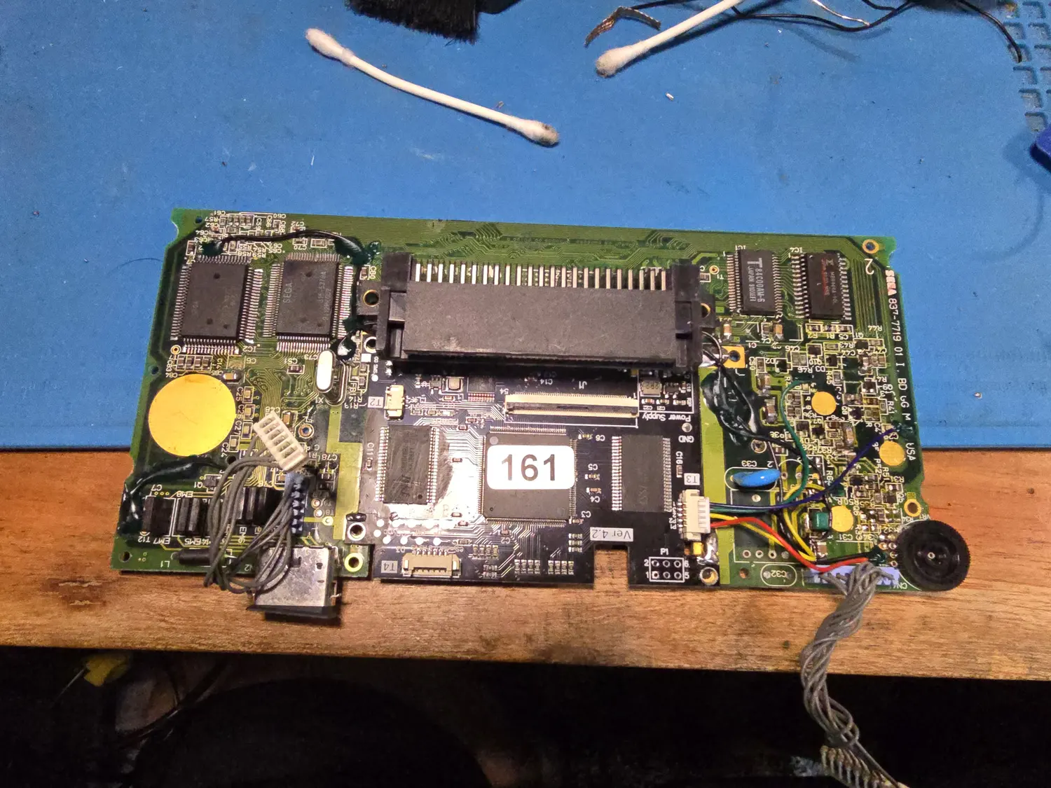
- Two custom chips near the speaker plus a separate, discrete Z80 CPU: that is a VA0 (the twin-ASIC board, all regions, roughly 1990 to 1993). It is the only revision with a discrete Z80. A flat plastic lens is a reliable tell that a unit is VA0.
- One big square custom chip (a 144-pin QFP) instead: read the number on it. A 315-5535 is a VA1 (single-ASIC, all regions, the last board for Europe and Japan). A 315-5682 is a VA4 or VA5 (North America only).
- To split VA4 from VA5, and both from the reissue: the case label model number is decisive. 2110K is a VA4; 2110G is a VA5, which includes the 2001 Majesco reissue (board 171-7923A).
What actually differs, and why it matters:
- VA0 to VA1 consolidated the Z80, video processor, and system controller into one ASIC, but from a screen standpoint the two are the same: both use the Citizen UC-320 LCD and the panel connections are identical. Two things follow. First, the OEM screen can be moved between boards. This page said the opposite for a long time, on the grounds that nobody had documented doing it. That was accurate right up until it wasn’t: Luke at RetroSix worked out a method and published it, and people are doing it routinely now. I was pointed at it by pizza_whistle and strra, who have both done it more than once. The clever part is that you never touch the joints: you tuck the screen under so the pins are pre-loaded to lift, brace it, then walk hot air down the row at about 420 C and 120 airflow, roughly a centimetre off, and the pins release themselves. The panel comes away with its pins clean and reusable. Treat this as advanced work with a hard tooling floor. You want a real hot air station and a soldering iron with proper closed-loop temperature control, JBC or equivalent rather than the approximate control on a cheap station, plus decent flux, solder, and electrical or Kapton tape. The ribbon is thin polyimide and copper with nothing to sink heat into, so an iron that overshoots or sags will melt it. Second, because the connections match, most modern screen kits cover both VA0 and VA1 with one product, so the ASIC count is mostly an install detail, not a different screen. The kit line that actually does not cross is VA4/VA5, below.
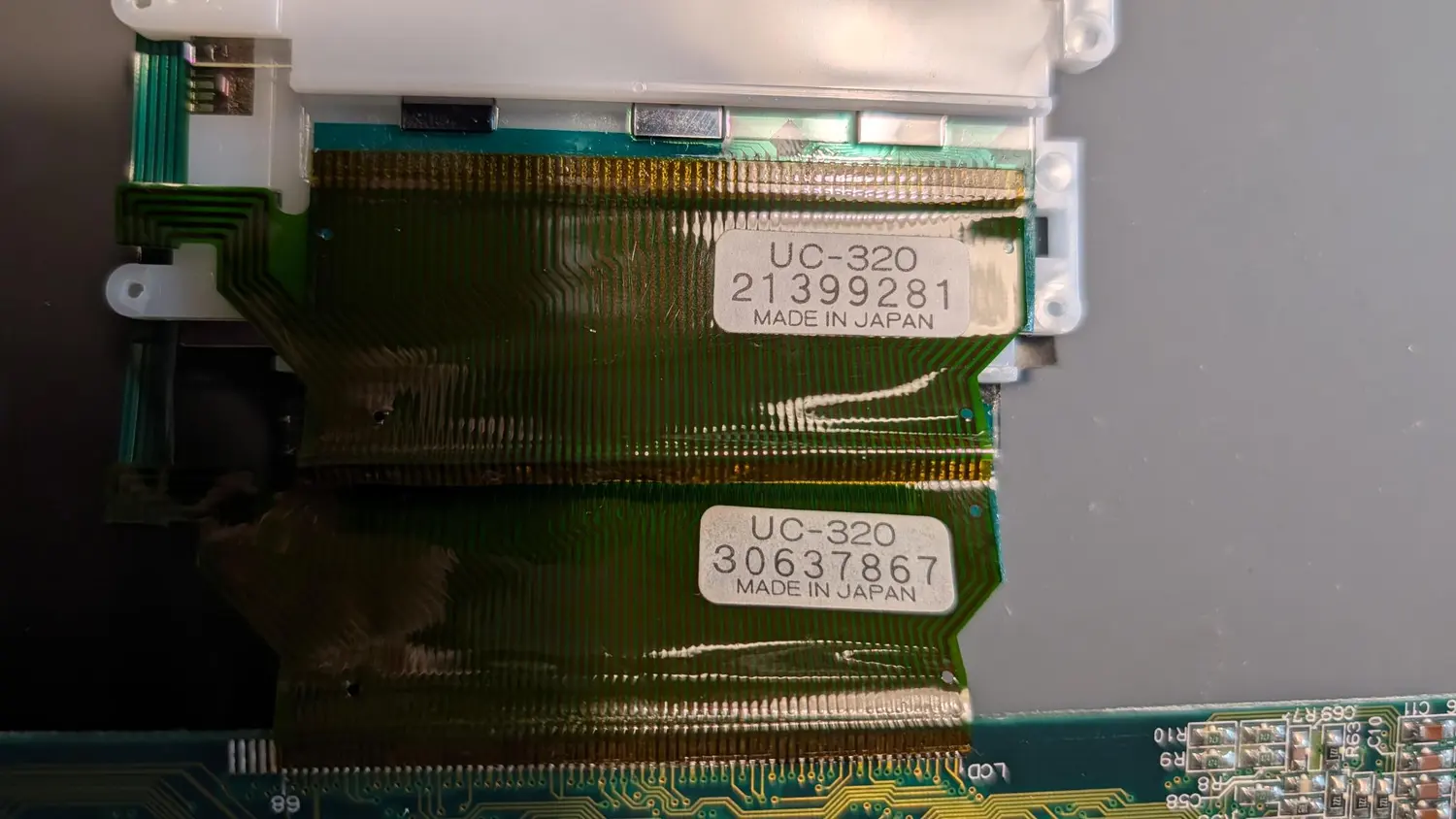
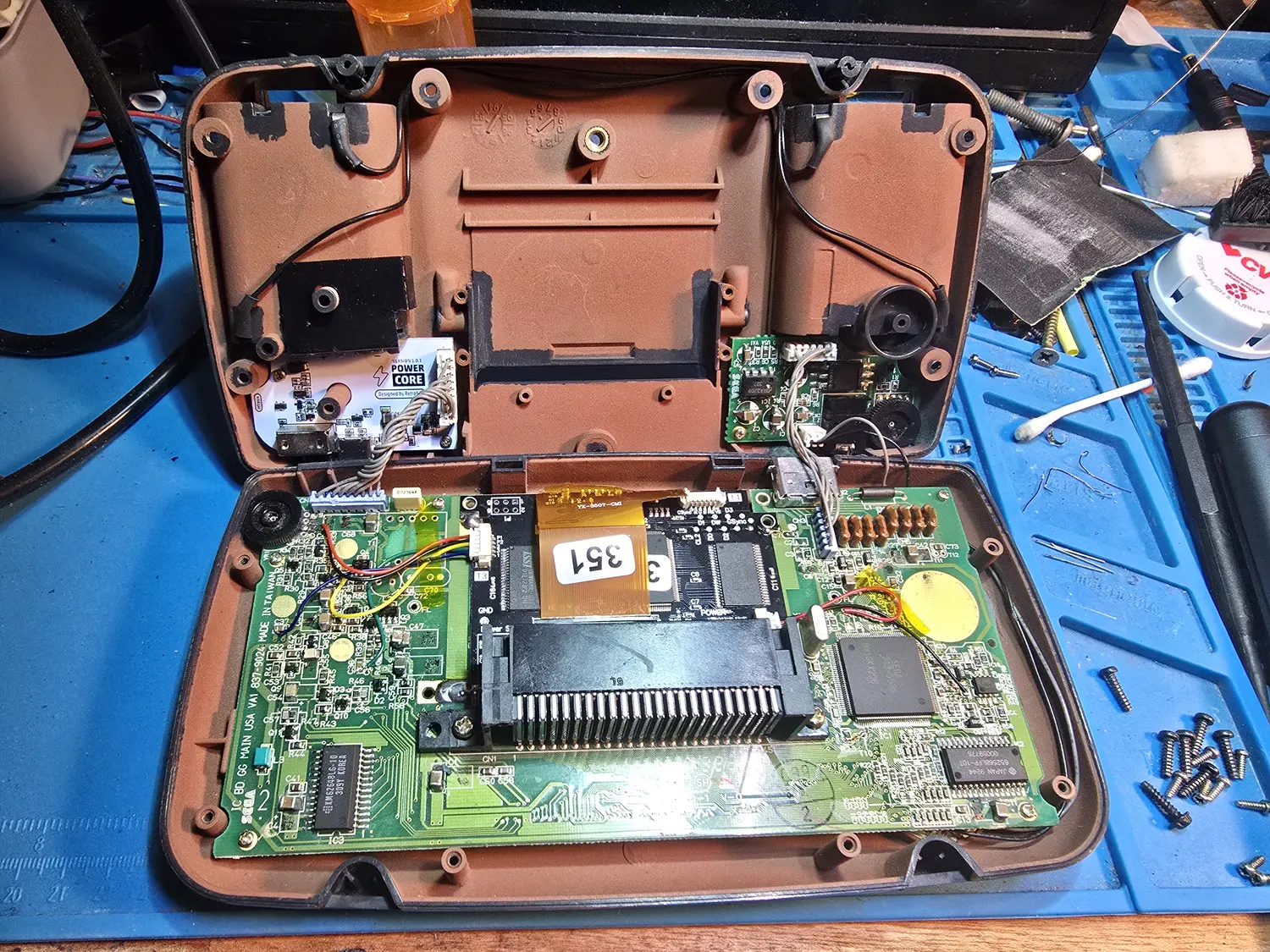
- The VA0 and VA1 panels are interchangeable, and somebody has now actually done it. I used to hedge this. Sega’s own drawings put the same signals on the same pins for both revisions, and one screen kit fits either, but a kit only takes over seven of the sixty-eight connector positions (9, 16, 18, 20, 39, 57, 68). Kit fitment could never say anything about the other sixty-one, and the panel uses far more of them than the kit does, so it stayed possible that the two differed somewhere no kit touches. On 25 August 2026, BlackLabelSupreme on r/game_gear moved a stock VA1 panel onto a VA0 mainboard and reported that it worked perfectly, adding that the LCD carries the same part number on both. A working OEM panel drives every pin it uses, which is exactly the test the kits could not perform. Better still, BlackLabelSupreme photographed the two panels together, the dead VA0 screen beside the VA1 screen now running on the VA0 board, and both are stamped UC-320. So this is not two similar panels that happen to be wired alike. It is the same Citizen part on both revisions, which is what the connector being identical implied all along. That is one swap rather than a survey, but it agrees with both Sega sheets, so treat a VA0 and a VA1 panel as the same part. Line up pin 1 to pin 1 and pin 68 to pin 68 on reattachment and check it before you close the shell.
- When you check a donor panel, match on UC-320 and ignore the number under it. Each label carries a second, eight-digit number below the part number, and those do not match: the pair in the photo below read 21399281 and 30637867. That is a per-unit serial, not a variant code. Two panels reading different eight-digit numbers are still the same part. Saying so here should stop someone binning a perfectly good donor screen over a number that was never going to match.
A real shock hazard, unlike a Game Boy
A word before you start poking around, because this is one of the few consoles I write up that can actually bite you. A Game Boy DMG is electrically harmless; you could lick any point in one and be no worse off than after lunch at Arby’s. The Game Gear is not that. It runs a +34 V rail to bias the LCD, and for the backlight it has a small inverter that steps the supply up into the kilovolt range to strike the cold-cathode tube. Both are live even when the console is running on nothing but AA batteries, because the power board boosts them up from the low-voltage supply. Pulling the wall adapter does not make it safe.
The +34 V rail alone will give you a solid, genuine zap. I have taken one or two of these, and in my experience it hurts like hell for about thirty seconds and then fades. It will not kill you, but it will get your full attention, and the real danger is that it makes you flinch into something you did not mean to touch. The two spots to respect most are the connections around the CCFL backlight tube and its inverter, which carry the highest voltage on the board, and the +34 V rail right at the power board.
So: keep one hand off the board when you probe a powered unit, do not let the CCFL leads or the bias rail surprise you while it is running, and power the console down before you move your hands or reposition it. And note the specific trap covered under the backlight section below: a standard oscilloscope probe on the inverter’s high-voltage side both mismeasures it and can inject a transient that latches the console’s ASIC.
Common problems and fixes
Recap first, almost always
Before chasing any of the symptoms below, deal with the capacitors on a unit that has never been serviced. Leaking surface-mount electrolytics are the Game Gear’s defining fault, and a clean board is what I trust before I believe any other measurement. I do not treat all three boards the same, though:
- Main board: every cap, every time. These are the leak-prone silver-can surface-mount electrolytics, and they all come out.
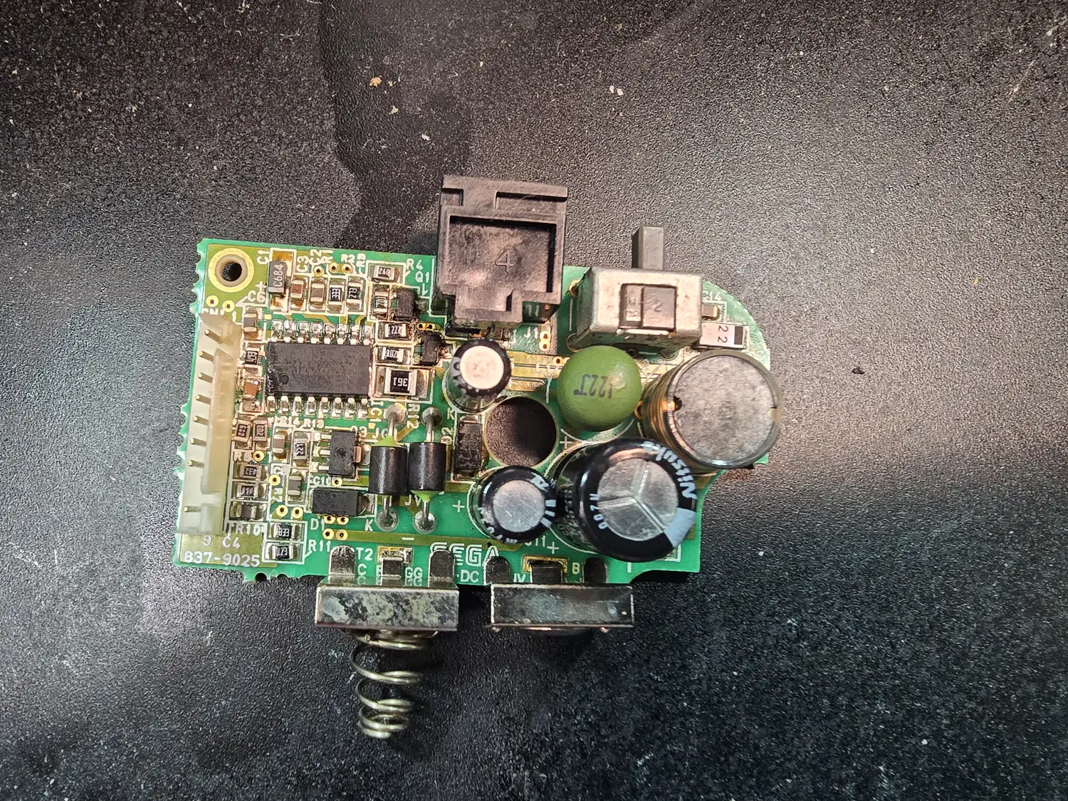
- Sound board: I usually do it too. Same type of cap, quick to reach, so it is cheap insurance.
- Power board: I inspect rather than recap on reflex. I have never personally found a leaking cap on a Game Gear power board, so a clean, good-testing one I will leave alone. But I keep the parts on hand and I do it if the board is already out, or if a power board comes to me dead, because I have seen dead power boards come back to life on a recap and nothing else.
One practice, plainly: with the single exception of the 820 uF power-board bulk, I replace every electrolytic on the Game Gear with a ceramic. Modern electrolytics are perfectly fine, but ceramics do not leak, they are easier to place, and they retire the whole capacitor-plague worry, so I see no reason not to. The only place a ceramic does not belong is that 820 uF bulk, a high-current, low-impedance spot that wants a proper low-ESR electrolytic. Never put a ceramic or a tantalum there.
Getting the old cans off without wrecking pads. This is the step that turns a clean recap into a trace repair, so do it deliberately. Do not desolder the cans in place, do not cut them off with flush cutters, and do not warm the joints and pull the can upward. All three load the pad in the direction it is weakest, and hot tweezers are no better.
What I do instead: grab the can with needle-nose pliers, push down, and twist and wiggle it back and forth in place until the legs fatigue and snap. The can comes away and leaves its legs behind on the pads. The legs then come off with an iron and fresh solder and flux, and the pads get wicked clean.
The reason it works is that a pad is copper foil bonded to the board, and that bond is much stronger in shear than in peel. Lifting concentrates the entire load at the edge of the pad. Twisting spreads it across the bond while fatiguing the thin leg, so the leg gives out instead of the pad. The downward pressure matters and is the part people drop, because it keeps the joint in compression while you work it. Heat works against you throughout, since the bond weakens as it warms. That is what makes heat-and-pull the worst of the options, and leaked electrolyte corrodes the solder so it stops taking heat, which is exactly what tempts people into adding more.
Work on a bare board. Take it out of the plastic case before you start so there is nothing to melt.
One thing I do differently from the videos below: for the leg left behind, I crack the capacitor’s plastic base off rather than bending the leg back and forth. That exposes enough to melt it straight off with no further stress on the pad. Once the can is off, you have won.
Credit where it belongs: this is Mr Carlson’s method, and I picked it up from Adrian Black at Adrian’s Digital Basement. The motion is the part that matters and it does not survive into text, so watch it:
- The method, and why desoldering a leaked board escalates (Macintosh Centris 610, from 8:53)
- The mechanism, shear with downward pressure (same video, from 34:00)
- Start to finish on a board that was not badly corroded (Amiga 1200, from 25:01, including the leg cleanup and a pad repair)
If you go looking for more of his, he calls it the twist method in the older videos and the wiggle method in the newer ones after viewers suggested the back-and-forth. Same technique, two names.
One caveat worth stating plainly: this is the best option, not a guarantee. Corrosion weakens pads, pads are only bonded to the board, and Adrian loses one occasionally and repairs it. Know the repair before you start.
Whatever you recap, the old electrolyte eats copper, so inspect for corroded traces and lifted pads under every cap you pull, and patch what you find.
Two caveats that save time. The later VA5 and Majesco units leak less, though it is still worth doing. And more important: a recap does not explain a dim backlight or a plain black screen. The references that push recap-everything do not blame the caps for those two symptoms, and neither do I. Those are separate faults, covered below. Recapping first is still worth doing because it clears the noise, but do not expect it to fix a dark or dead display on its own.
No sound, or the speaker is dead but headphones work
A speaker that is silent while headphones play fine is a good, narrow clue. It puts the fault in the speaker itself, the two-pin speaker connector, the headphone jack’s cutoff switch (which mutes the speaker when a plug is inserted), the speaker-enable line, or one channel of the TDA2822M amplifier on the sound board. If there is no sound from either output but the picture is fine, look instead at the audio chain feeding the amp: the sound generator, its filter network, the op-amp buffer, and the analog supply.
In practice the fix is a recap of the sound and power boards, plus reflowing or repairing the inter-board connector and patching any corroded traces. Bad capacitors are the most common cause of low or missing audio here.
No power, or it powers on then immediately shuts off
Confirm the power source before you open the board, because the Game Gear’s power jack has a trap in it (see the polarity warning below). Then walk the rails: you are looking for a healthy +5 V and a +34 V at the power-board harness. The +34 V is the LCD bias rail, and it is worth knowing it exists this early because a fault there presents as a display problem, not a power one.
The usual causes, in rough order: bad capacitors again (the large 820 uF bulk capacitor on the power board is the first to suspect for a brown-out or a won’t-stay-on symptom), corrosion on the AA battery terminals from leaked cells, damaged wires or cold joints on the power-to-mainboard connector, and a loose or worn DC jack. Clean battery corrosion with a mild acid such as distilled vinegar followed by isopropyl alcohol, reflow the jack with fresh solder, and recap.
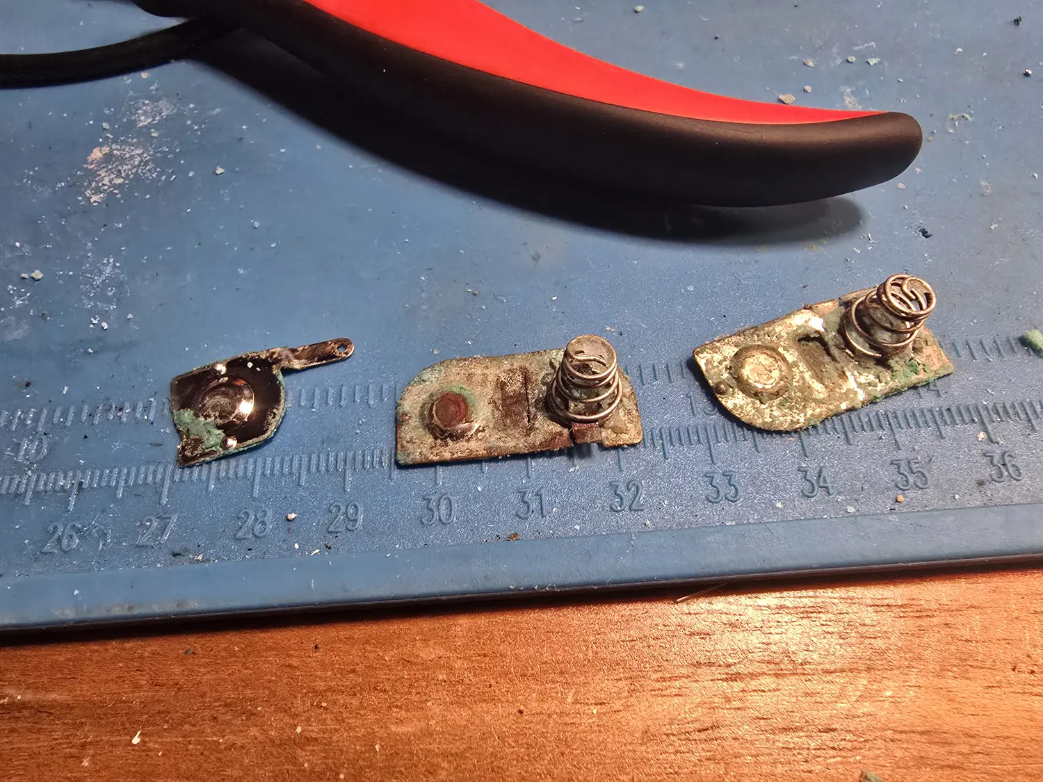
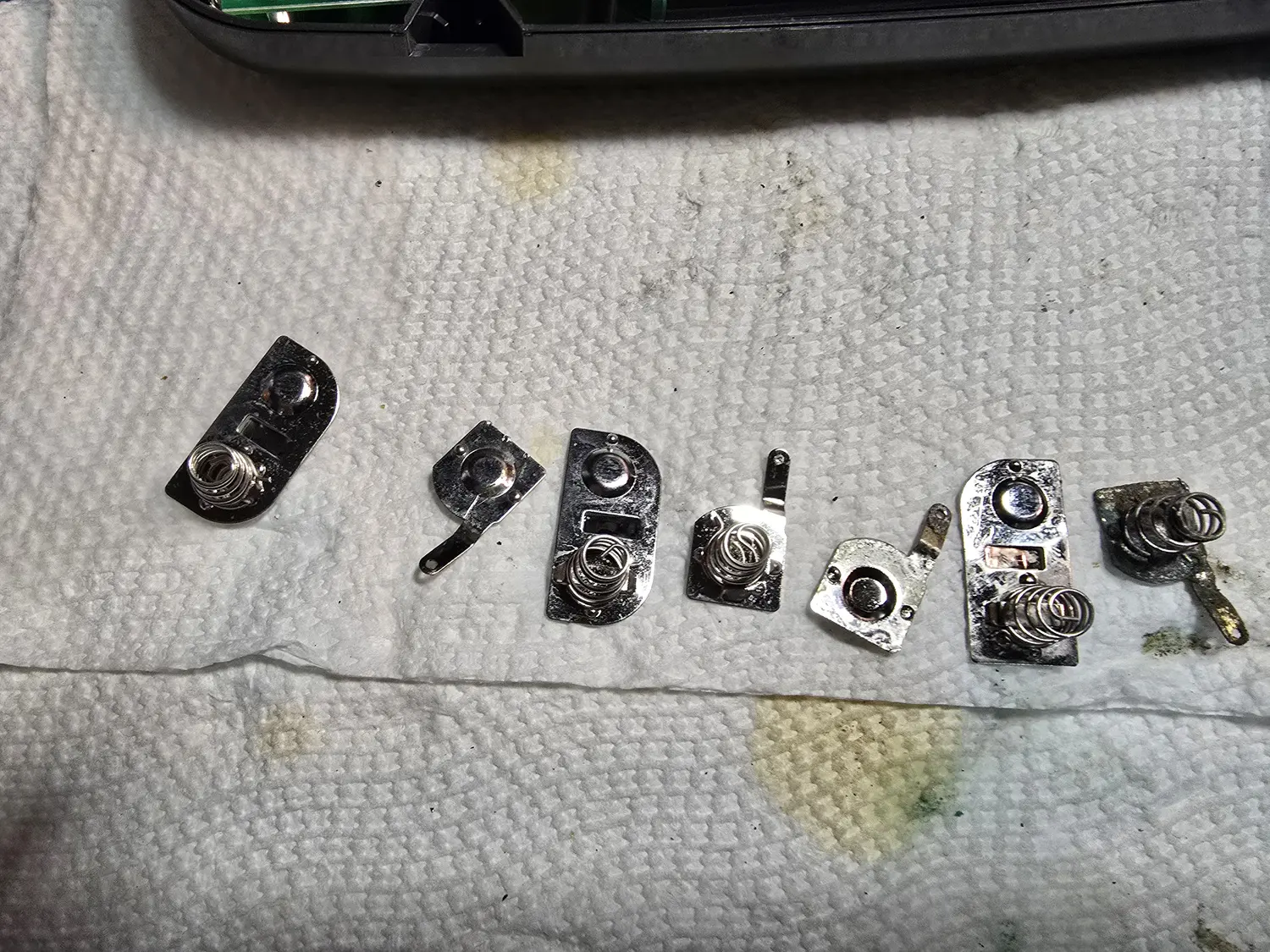
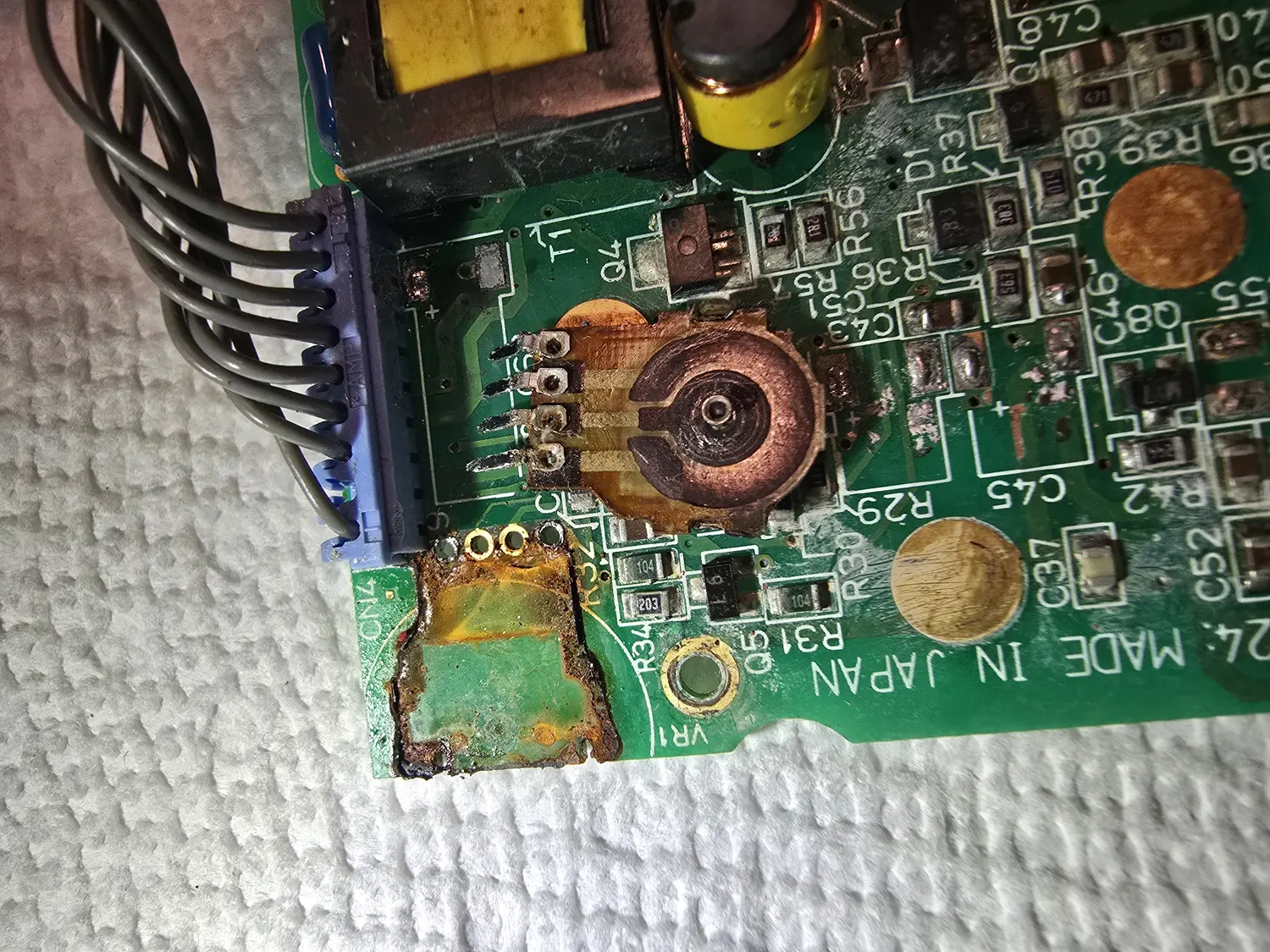
One mechanical gotcha: the DC jack has a built-in switch that disconnects the AA batteries when a plug is inserted. If that switch is bent or corroded, you get a “batteries do nothing, adapter is fine” fault that is mechanical, not electronic.
The power-jack polarity trap. The Game Gear’s DC jack polarity is not the same worldwide, and it does not follow the NTSC/PAL video standard the way you might guess. It follows the mains region:
- North American units are tip-positive, on the smaller 4.75 / 1.7 mm EIAJ-03 barrel, at 9 V.
- European units are tip-negative, on a physically larger 5.5 x 2.1 mm barrel, at 10 V.
- Japanese units are also tip-negative, on the larger barrel, even though Japan is an NTSC region. This is the trap: you cannot reason from the video standard to the plug.
The voltage is a different split from the plug, and this catches people out. The jack divides on mains area, and Japan groups with Europe there. The voltage does not: Japan is an AC100V country, outside both of the columns in Sega’s own service manual, and ships its own 9 V adapter. So it is 9 V in North America, 9 V in Japan and 10 V in Europe, and what Japan actually shares with Europe is the polarity and the barrel, not the voltage. Region-to-voltage is stable per adapter part number and era rather than per region anyway: the same service manual ships 9 V bricks to the UK and to Australia.
The practical consequence for anyone building or buying a USB-C adapter: a 9 V supply is exactly OEM for a Japanese unit, and it is inside the envelope for a European one too, because the console is designed around a 9 V nominal source. Six AA cells are 9.0 V, Sega’s own battery pack is specified DC 9 V in, and the series input diode drops the DC-DC input to roughly 8.1 to 8.5 V from a 9 V supply either way. The blocker on a European or Japanese unit is the polarity and the barrel size.
The polarity also does not track the board revision (both one-ASIC and two-ASIC North American units are tip-positive). So do not infer polarity from anything except the market the unit was sold in, and when in doubt, measure the jack or identify the barrel size before you connect a supply. A wrong-polarity adapter is a common way people brick these. The console’s series input diode normally blocks a reversed supply so the unit simply will not turn on, but if that diode has failed shorted, the protection is gone.
Audio plays but the screen is wrong
One of the most useful splits on the bench. If the game’s sound is playing normally while the screen is black, washed out, or garbled, a large part of the console is proven good in one shot: the CPU is running, the cartridge and slot are making contact, and the 5 V rail is up. That corners the fault into the display path, and it is almost always one of two things: the screen-related capacitors are bad or were fitted wrong, or the panel is dead.
Work the caps first. The LCD bias ladder (on a VA1 that is C45, C47, and C49) is value-sensitive, so a leaked cap, or the wrong value fitted during a recap, will keep the picture from coming up right. Confirm those before anything else. If a clean, correct bias recap does not restore the image, do not write the screen off yet: confirm the drive signals are actually reaching the panel, the roughly 5.38 MHz data clock, the bias rail, and the TPR and sync lines. I have saved a screen right here. On one repair the entire drive chain scoped perfectly, which told me the electronics were fine, and the real fault was mechanical, the LC panel had drifted off its backlight (the black-screen section below has the full check). Proving the signals good is not a dead end; it is what tells you to stop chasing the electronics and look at seating, illumination, or the panel itself. Plan a screen kit only after the caps are confirmed and the drive signals are present.
Dim or dark backlight
The Game Gear lights its LCD with a cold-cathode fluorescent tube driven by a small high-voltage inverter, and this is where dim and dead backlights come from, not from the main filter capacitors. A backlight that has gone dim and pink with age is usually the tube itself wearing out. A fully dark backlight points at the inverter circuit or its dedicated supply.
Some community references single out a couple of small backlight-circuit capacitors for the specifically dim (not dead) case, so a recap is a reasonable first pass before condemning the inverter. But treat the tube’s own aging as the more likely cause of a dim glow.
There is one hard safety rule here. Do not put an ordinary oscilloscope probe on the inverter’s high-voltage secondary, its coupling capacitor, or the lamp leads. That node runs kilovolt-range peaks, and a standard probe both fails to measure it correctly and can inject a transient that latches up the console’s ASIC, freezing the game until you power-cycle. On my own bench that latch-up is exactly what happens, and it looks like a fault you just caused rather than one you are diagnosing. Use a proper high-voltage probe, or work the low-voltage primary side of the inverter.
A useful rule the other direction: if the backlight glows at all, the inverter is running. So a black screen with a lit backlight is not a backlight fault. That one gets its own section. Read the rule as a rule-out and nothing more, though: a glow tells you the inverter is producing output, not that it is healthy. A dim glow is still consistent with a degraded C70 or an aged tube.
Black screen with the backlight on
This is the high-value diagnosis, and a common fault. The backlight is lit, so you know the inverter is running, and yet the image is solid black. Work it cheap-and-mechanical first, and save the oscilloscope for last.
- Check for a cartridge, and reseat the panel. A Game Gear with no cartridge shows black anyway, so put a known-good cart in first. And the LC panel can physically drift off its backlight assembly after a repair, which reads as dead-black while the whole drive circuit is perfectly healthy. Shine a light through the panel from behind: if you can see a clean image in the transmitted light, the electronics are fine and the fault is seating or illumination.
- On a later board, retest with a known-good licensed cartridge. The VA1 from 1993 onward, and the VA4 and VA5, carry a Sega boot ROM (TMSS) that holds the screen off and locks the console if the cartridge does not carry the expected Sega header. A dirty slot, a bad contact, or a pirate or repro cart can therefore produce a black screen with the backlight on that is indistinguishable at a glance from a hardware fault. A clean, licensed cart rules it out.
- Suspect a VA1 ground fault, early. This is my specialty on these boards and the thing that fools people: a cracked ground via starves the LCD bias section, which floats its output toward +5 V and pins the screen uniform black while the bias regulator itself measures perfectly. It is ground starvation wearing a bias fault’s clothes, and I have traced it on more than one unit. It earns its own writeup, just below.
- Then the bias caps, the contrast pot, and the ribbon. A leaking or cold-jointed capacitor in the bias ladder skews a tap and blacks the screen, which the recap-first pass should already have addressed. A scratchy or damaged contrast potentiometer, a damaged LCD ribbon, or corroded traces round out the list.
One thing not to do: do not reflexively reflow the LCD ribbon on a uniform black screen. Full-black with everything else working points at the bias path, not the ribbon. The ribbon is the suspect for missing lines, not a blacked-out picture.
The VA1 floating-ground fault
If you fix Game Gears in any volume you will meet this one. The VA1 board’s ground distribution is not robust: however Sega stitched these grounds, they crack, split, and lift far too easily, and a lost ground reference produces symptoms that look exactly like a dead active circuit. I have traced it on more than one unit.
What it looks like. A section’s output rail sits pinned near +5 V while the generator or regulator feeding it measures perfectly healthy. That is the signature of ground starvation, not a dead circuit: with no ground reference, the output floats up to the +5 V rail. The classic case is the LCD bias output sitting at +5 V with a perfect bias regulator, which reads like a bias fault and is not one. The screen goes uniform black with dead contrast while power, audio, and backlight are all fine.
Where it comes from. Three ways I have seen it:
- A cracked ground via on one of the bare golden pads under the button standoffs, near the contrast wheel. On one unit that pad was the ground for C36, the decoupling cap on the ASIC TPR2 output, and the open via floated the bias section. Those pads flex and take thermal cycling, so they crack.
- A whole side of the board losing its ground tie to the other side, which turned up midway through an IPS screen install.
- Ground copper lifting from board delamination when the big CCFL inverter transformer (T1) is removed with too much heat. Go easy on heat around T1; it delaminates and takes ground with it.
One thing that trips people up: those golden standoff pads are each grounded by their own independent via and are not joined to each other on the surface. So a good board will not show continuity from one pad to the next, and that is normal, not a fault. A cracked via floats just its own pad toward 5 V while its neighbors sit at 0 V.
How to confirm it safely. Ohm the suspect pad to +5 V: a real short reads ohms to a few kilohms, while a floating ground reads megohms, which tells you it is safe to tie to ground. Then toggle-test: clip a jumper from the starved node to a known good ground and the screen comes to life; pull it and the screen goes dead. That locks causation.
The fix. Flywire the starved ground to a solid ground, landing it on a component terminal rather than a fragile bare pad. The negative terminal of a big nearby SMD capacitor makes a good anchor, but verify it reads near zero ohms to a known good ground first. Route the wire clear of the button-standoff crush zones, since the standoffs press hard there, and strain-relieve it with a dab of epoxy, not solder mask, which is insulation and not an adhesive. Dry-fit the case and standoffs before you close up so the wire cannot get pinched or drift off again.
Dim, washed-out, or rolling picture
Distinct from a dim backlight, a dim or washed-out or rolling image with the backlight clearly on is a bias-circuit problem. Recap the bias filter capacitors first, then check that the contrast potentiometer sweeps its full range, and compare the bias taps against a known-good board. There is no OEM per-tap voltage table, so a reference board is the practical way to know what “right” looks like. Rolling or non-static lines belong here too; that is a bias-cap symptom, not a ribbon one.
Missing part of the picture
A missing vertical band of the image, a whole third gone or driving differently from the rest, is a failed column driver for that segment of the panel. In my experience this is not a repair. Those driver ICs live on the panel’s own ribbon, not on a board you can rework, and I have never seen one of these vertical-band failures come back. Unless you can trace the fault to something on the mainboard feeding the panel, plan on a screen replacement. Some references describe the driver ICs as discrete and reworkable on certain revisions; I have not been able to make that repair succeed, so I would not count on it.
Missing thin lines, Game-Boy style, are the LCD ribbon connection detaching. Important and often gotten wrong: the Game Gear’s mainboard-to-LCD ribbon is soldered copper flex under a Kapton strip, not a heat-seal bond. So you reflow it with a soldering iron or lift and refit it with hot air. The “heat-seal melts at 190 C, cannot be soldered” rule that circulates for these is Game Boy DMG lore and does not apply to the Game Gear mainboard joint. On a VA4 specifically, the thin wires joining the ribbon to the motherboard are fragile, and breaking one is how you create missing lines rather than fix them.
Stuck or dead pixels
A scatter of individual pixels stuck on, often green in my experience, is a panel fault rather than a board fault. In my experience these survive a recap and are simply dead pixels in the LCD, so a screen kit is the only reliable fix. I will soften that only slightly, because it is not quite absolute: people do try to revive stuck pixels by gently warming the edge of the panel, and there are reports of it helping, but also of the pixels returning soon after, so treat it as a temporary long shot rather than a repair, and remember that heat near the panel and ribbon can create fresh damage. Static pixel faults that outlast a recap point at the panel or its driver, not the board. If the unit needs a clean screen, plan on the kit.
Won’t play a cartridge
The Game Gear has no region lockout chip and (on VA0) no boot ROM, so a cartridge boots straight from the processor. A won’t-boot cart is therefore almost always a power, bus, or slot problem: dirty contacts on the 45-pin slot, a broken address, data, or control line, or missing +5 V or clock at the slot. Clean the slot and the cartridge edge, and verify the rails and clock reach it.
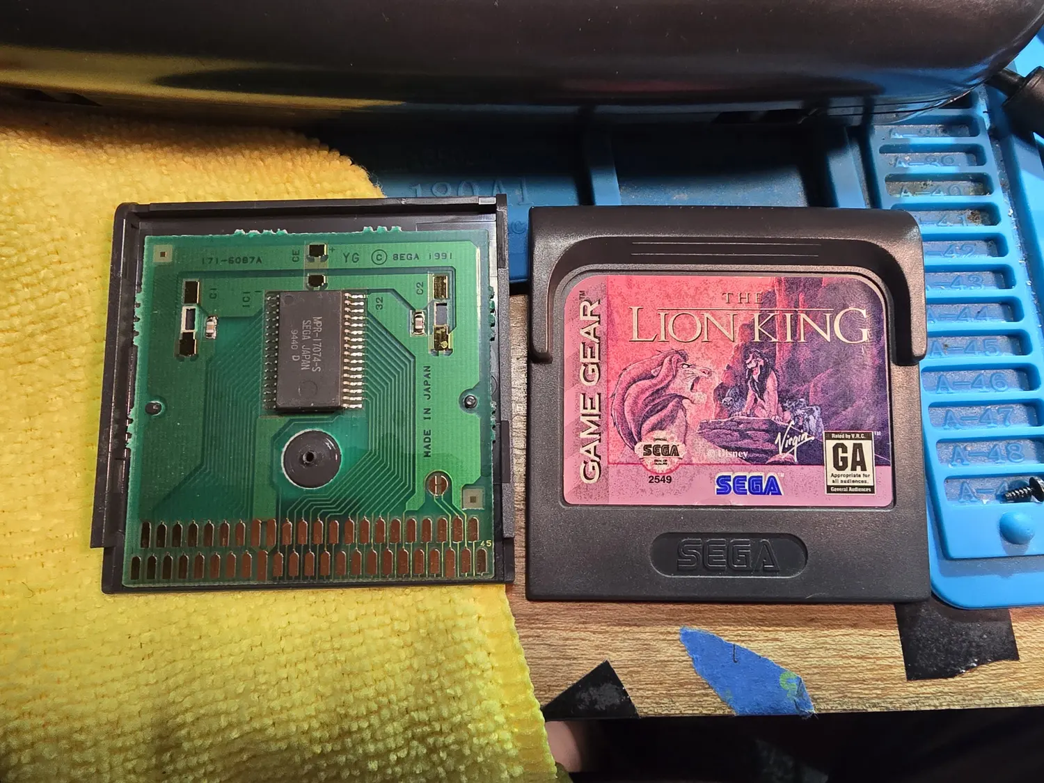
“Almost always,” not “never,” because there are two real exceptions. On the later boards, the TMSS boot ROM described under the black-screen section can lock the console on a bad or unlicensed cart. And there is exactly one commercial cart, the Japan-only Pop Breaker, that reads the console’s region flag carelessly and will not get past its title screen on a non-Japanese unit. Neither is a common field problem, but both are worth knowing before you condemn a slot.
Inside the Game Gear
A short tour of what the hardware is doing, which makes the faults above make sense.
- Three boards, not two. The Game Gear splits into a main board, a separate DC-DC converter (power) board, and a separate sound board. This matters for a practical reason: the reference designators restart on each board, so a “C5” or a “Q3” means different things depending on which board you are looking at. Always name the board.
- Two rails run the machine. The power board makes a +5 V logic rail and a +34 V rail that biases the passive-matrix LCD. The LCD needs that high bias voltage and an alternating drive because of how STN panels work, which is why there is a whole bias ladder to go wrong. The +34 V is also exposed on the cartridge edge, so a shorted accessory can drag it down and look like a display fault. One thing worth knowing before you sink hours into a dead +34 V rail: it is needed only by the OEM screen. Every modern screen kit generates its own bias and does not touch the +34 V, so if the +5 V rail is good and the game plays in the background, a stubborn bias-rail fault is not a dead end. I will still try to fix a bad +34 V before giving up, but worst case you kit the screen and the problem disappears. And if you do want the rail back, a RetroSix PowerCore board is only around 18 dollars and carries a +34 V rail you can switch on or off.
- The digital core consolidated over time. VA0 spreads the Z80 CPU, the video processor, and the system controller across separate chips, which means you can bisect a dead VA0 chip by chip. VA1 onward folds them into a single ASIC, so a dead-but-powered later board is more of an all-or-nothing part, and you lean harder on the rails, the clock, the reset line, and the recurring ground faults first.
- One crystal runs everything. A single master oscillator feeds the whole ASIC. If it is dead or badly loaded, you lose the CPU, video, and sound all at once, so scope it for a clean oscillation before you condemn a 144-pin chip.
- The backlight is independent of the image. The cold-cathode tube and its inverter run off their own gated supply, separate from the +34 V bias, which is why the backlight can be alive while the image is dead, or the reverse.
Mods worth knowing
I do not reproduce anyone’s install guide here. This is an overview of what is worth doing and where to go for the real instructions. The screen mod is the headline, and everything about it comes back to the board revision, so identify the board first.
- LCD / IPS screen replacement. This is the flagship upgrade and the biggest resale value-add. Modern kits digitally capture the video and rescale it, so the picture is sharp with no lag, and installing one removes the old CCFL inverter, which is the console’s biggest battery drain. Compatibility splits on the panel, not the ASIC count: VA0 and VA1 share a panel, so most kits cover both, while VA4 and VA5 need their own. The kit I have the most hands-on time with is the FunnyPlaying, which resembles the original McWill, works on VA0 and VA1, and ships with a ribbon cable that makes the solder job easier; it wires to the contrast wheel and the face buttons and changes display modes by button combinations, with no on-screen menu. It is AliExpress-only and runs about 50 to 60 dollars.
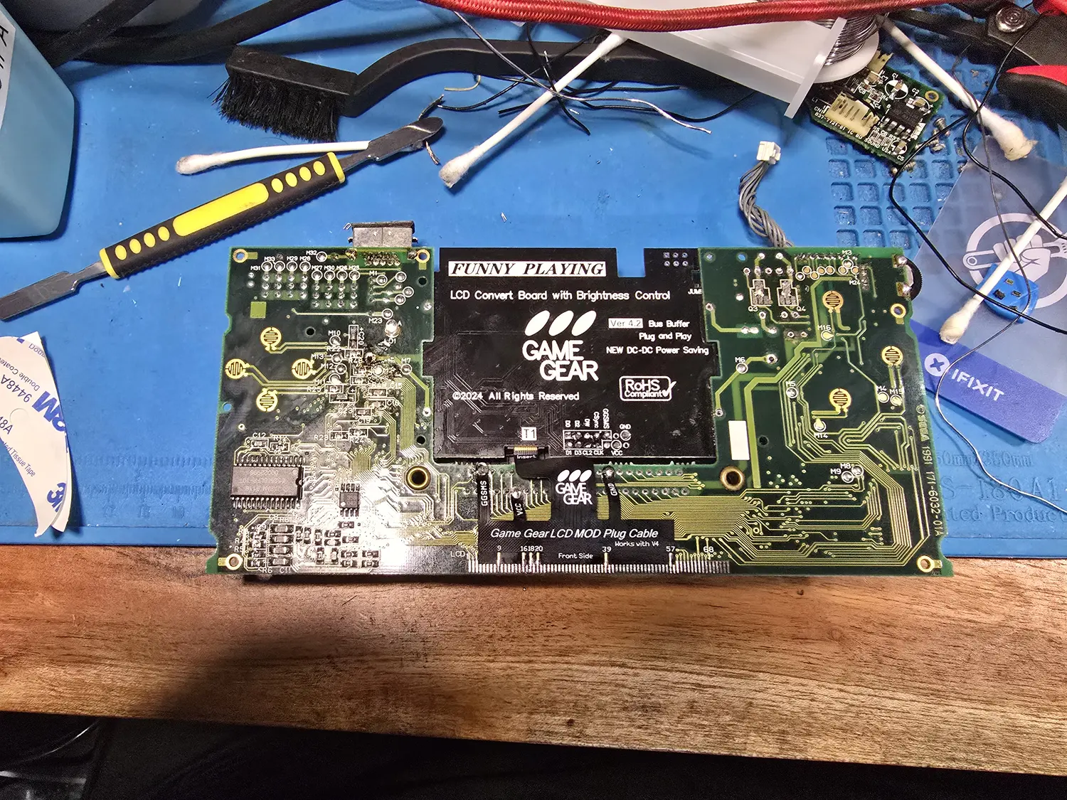
The Hispeedido 3.5-inch laminated IPS (through HandHeldLegend) is the one I expect to move to: a larger 640x480 laminated-glass panel with a real on-screen menu and, by reputation, the better picture. The original McWill (through 8bitmods and Retro Modding) is still sold, as separate, non- interchangeable VA0 and VA1 variants with their own soldered install guides. BennVenn’s VA0/VA1 flex kit is the wire-light option, and BennVenn also makes the go-to kit for the North American VA4, VA5, and Majesco boards, which no VA0/VA1 kit fits. RetroSix’s CleanScreen aims to cover every revision from VA0 to VA5 in one line. Confirm the panel revision before you buy; for VA0/VA1 the ASIC count only changes the install steps, not the screen. One vendor detail worth carrying over even where the kit does not mention it: confirm the 5 V rail is not above 5.45 V before you fit any digital-capture panel, because a failed regulator can destroy the new module. References: McWill via 8bitmods, Hispeedido kit at HandHeldLegend, BennVenn, and the RetroSix Game Gear wiki.
- Telling the screen mods apart on a used unit. If someone else already modded a Game Gear and you want to know what is in it, a few tells help. A panel noticeably larger than stock, filling the bezel edge to edge behind flat laminated glass, with an on-screen menu (on a Hispeedido, hold Start plus 1 plus 2 to open it), is a Hispeedido or a similar 640x480 laminated kit. A roughly OEM-sized panel with no on-screen menu, where display modes change by blind button combinations, is a FunnyPlaying. The original McWill runs a smaller 320x240 native panel unless it was fitted with McWill’s optional 3.5-inch IPS. And a panel with an obvious air gap between the image and the lens, or a poorly printed lens, is usually a budget AliExpress kit, which is a mark against the unit.
- USB-C power. You can convert the Game Gear to USB-C, either with an external dongle into the barrel jack or with a replacement power board such as the RetroSix PowerCore that adds an onboard USB-C port. A caution from my own bench: a bare “PD trigger” dongle that just requests 9 V and passes it through will boot-loop on strict or Apple-grade USB-C chargers, and it is not a capacity problem (the console only draws about 3 W). The robust approach takes the default 5 V that any USB-C source provides at attach and boosts it internally, which skips the power negotiation entirely.
- Internal rechargeable battery. With a low-draw IPS/LED conversion in place, an internal lithium module (such as the RetroSix CleanJuice) becomes practical where the stock CCFL draw made it painful. Treat any lithium install as safety-relevant: correct cell, protection circuitry, and no heat or crush near the pack.
- TMSS boot-screen skip. On the boards that have the Sega boot ROM, you can disable the splash and speed up boot by bridging a jumper pad on the mainboard. It is a one-solder-bridge job and a nice finishing touch, but it does not fix any cartridge compatibility problem on the Game Gear, so it is cosmetic.
Recap and parts
The recap is the center of gravity for Game Gear parts, because leaking surface-mount electrolytics are the defining failure. A VA1 has about 20 electrolytics across its three boards; the VA0 is similar. VA4, VA5, and Majesco have their own cap maps, and the kits are not interchangeable between revisions, so order by board number.
A few practical notes:
- Buy a revision-matched kit for volume work. Vendors sell a Game Gear cap kit that covers the VA0/VA1 main, power, and sound boards, and separate kits for VA4 and for VA5/Majesco. They replace the surface-mount cans with radial-lead capacitors, which are more robust and easier to source. Confirm the board silkscreen before ordering, because a VA4 kit will not fit a VA5.
- Every cap but one goes ceramic. With the single exception of the 820 uF power-board bulk, every electrolytic on the Game Gear can be replaced with a ceramic, and that is what I do. The larger values are not a problem: 100 uF ceramics in 16 V and even 25 V are readily available, and while they are not cheap, up to about 80 cents each, that is still perfectly reasonable for the handful on one console. Size the voltage rating up to cover DC-bias derating, use an X7R or X5R dielectric, and you get parts that do not leak and are easier to place. The one hard exception is that 820 uF bulk: it is a high-inrush, low-impedance spot that wants a proper low-ESR aluminum electrolytic, never a ceramic and never a tantalum, which can fail short there.
- The parts that are effectively unobtainium. The main ASIC is not replaceable, there is no source and no cross-reference, so a dead ASIC is a donor-board job. The Citizen UC-320 LCD is salvage-only and revision-locked. On a fleet, your worst board is your parts stock.
- The known non-cap consumables. Beyond capacitors, the parts a Game Gear repair actually consumes are the CCFL tube (superseded by LED/IPS mods for resale), the contrast potentiometer, the audio amplifier, and occasionally the DC jack. Match the DC jack’s polarity to the region, per the warning above.
The hard data behind all of the above (the per-board cap maps with substitutes, the non-cap consumables, the LCD and ASIC pinouts, and the schematic facts) is tabled in the sections that follow. Long per-item notes fold away to keep it readable; expand any of them for the full detail. The cap maps are VA1 so far and the other revisions follow. The pinouts now cover two revisions: the VA0/VA1 68-pin panel connector and the ASIC, and, new, the VA4 LCD driver interface, which I reverse-engineered on my own bench because no OEM VA4 service manual or schematic exists. That means the three 21-pin column-driver flexes along the bottom of the panel, the two 11-pin row-driver flexes on the right, the clocks and bias rails on both, and the MC34063A at IC4 that turns out to generate the VA4’s high-voltage rail on the main board itself. It is single-board bench data, tagged as such, and a fair amount of it is still open. I have marked what is open rather than rounding it off.
If you would rather buy a Game Gear that has already had this work done, everything I restore is in the shop. (I will link specific Game Gear service and recap-related listings here as those pages firm up.)
Probing a VA4
There is no VA4 schematic, so if you go after one of these you are measuring, not reading. Four things cost me real time on my own VA4 and will cost you the same.
A floating scope-probe ground turns the probe into a 60 Hz antenna and invents waveforms. On the row-driver bias pins it manufactured a clean, convincing 154 to 160 V peak-to-peak sawtooth, and I built a whole wrong hypothesis on top of it. Properly grounded, those same pins are static DC levels of 30 to 40 V with no AC on them at all. Land the ground clip solidly and close by, then touch nothing and confirm the trace is flat before you believe any waveform. This is the same failure that once gave me a phantom plus or minus 85 V on a VA1.
A multimeter averages the switching pins into fiction. Mine reported 34 V and 39 V on the row-driver pins where the scope showed the real levels. The column cable does it too: pins 17, 18 and 20 all meter around 5 V, and the scope shows pin 18 sitting flat at 0 V. Scope anything that might be switching, and when the meter and the scope disagree on this panel, the scope is right.
The contrast pot reads about 1.2 kilohms end to end in circuit, not its rated 20 kilohms. One end is grounded and the bias ladder parallels the element, so 20k in parallel with about 1.2k is what your meter sees. A second board read 1.7 kilohms. Both are healthy. Do not diagnose a wrong-value pot from an in-circuit reading; lift one leg if you want the real number.
The row-driver pin numbering is easy to get off by one, and I did exactly that on a first pass before a recount under magnification, which Sega’s own silkscreen then confirmed. Count under magnification and check that pin 2 reads ground before you trust the map on any board. Pin 2 is your anchor.
One more thing worth knowing before you start: the five VA4 driver ICs, three along the bottom and two on the right, are unmarked chip-on-board epoxy blobs. There is no part number on them and no datasheet exists, so there is nothing to look up. Measurement is the only route, which is why the tables below exist.
Capacitor lists
The per-revision electrolytic maps, with OEM part numbers and the substitutes I fit. Expand any row’s notes for the per-cap detail.
VA0 VA0 (twin-ASIC + discrete Z80)
Board p/n: 837-7719-01 (US) · 837-7996 (EU) · 837-7398-01 (JP)
VA1 VA1 (single-ASIC, 315-5535)
Board p/n: 837-9024 (US) · 837-9130 (EU) · 837-8560 (JP)
Main board — electrolytics
| Desig | Value | V | OEM p/n | Substitute | Note |
|---|---|---|---|---|---|
| C1 | 33µF | 6.3V | 150-0311 | 10V polymer or ceramic (X5R/X7R), size V up for DC-bias derate | ✓va1-sm,console5 |
| C4 | 10µF | 6.3V | 150-0308 / 150-0420 | 1206 X5R/X7R ceramic, ≥16V (a 10µF/50V 1206 drops in cleanly) | console5 lists an alt 16V; ceramic-substitutable ✓va1-sm,console5,leadedsolder |
notes on C4leadedsolder converted the 10µF positions (C4/C11/C14/C42) to
10µF/50V 1206 ceramic. This is one of the positions those sources
call cleanly ceramic-convertible. | |||||
| C11 | 10µF | 6.3V | 150-0308 / 150-0420 | 1206 X5R/X7R ceramic, ≥16V | alt 16V; ceramic-substitutable ✓va1-sm,console5,leadedsolder |
| C14 | 10µF | 6.3V | 150-0308 / 150-0420 | 1206 X5R/X7R ceramic, ≥16V | alt 16V; ceramic-substitutable ✓va1-sm,console5,leadedsolder |
| C42 | 10µF | 6.3V | 150-0308 / 150-0420 | 1206 X5R/X7R ceramic, ≥16V | alt 16V; ceramic-substitutable ✓va1-sm,console5,leadedsolder |
| C43 | 22µF | 6.3V | 150-0309 | I use ceramic (size V up); sources say keep electrolytic/tantalum | sources call 22µF+ a keep-electrolytic spot ✓va1-sm,console5 |
notes on C43Source stance (leadedsolder / retrorepairsandrefurbs): 22µF and up
should stay electrolytic/tantalum because 1206 MLCCs DC-bias-derate.
My bench differs: I run ceramic on everything but the 820µF bulk,
sizing voltage up to cover the derate. The “keep electrolytic” line
is what those sources say, not the recommendation here. | |||||
| C45 | 4.7µF | 35V | 150-0307 | 4.7µF ≥35V (bias-ladder cap: value-sensitive) | LCD bias ladder: a wrong/leaked value skews bias → uniform black ✓va1-sm,console5,mem-bench |
notes on C45Part of the LCD bias filter (C45/C47/C49). My bench: a leaked or
wrong-value cap here keeps the picture from coming up right while
the bias regulator still measures fine. Confirm before condemning
a panel. | |||||
| C47 | 68µF | 6.3V | 150-0318 | I use ceramic (stack 47+22 or use polymer); sources: keep electrolytic | LCD bias ladder cap ✓va1-sm,console5,mem-bench |
notes on C47Bias-ladder filter cap (see C45). Stack a 47µF base with a 22µF or
33µF make-up (33+33 ≈ 68; 33µF is the more available E6 stock).
Current sinks, so exact value isn’t critical: use whatever pair is
in stock. | |||||
| C49 | 100µF | 4V | 150-0319 | KEMET T520B107M010ATE070 (100µF 10V case-B polymer tantalum) | LCD bias ladder cap ✓va1-sm,console5,mem-bench |
notes on C496.3V-class rail, so the 10V polymer covers it. My settled 100µF
part (2026-07-21): the case-B (3528) polymer drops into tight pads
a 6032 would overhang. OEM can code MF4FC100D10. | |||||
| C54 | 0.47µF | 50V | 150-0317 | 0.47µF ≥50V ceramic | ✓va1-sm,console5 |
| C55 | 0.47µF | 50V | 150-0317 | 0.47µF ≥50V ceramic | DESIGNATOR COLLISION: VA4's C55 is a different part entirely ✓va1-sm,console5,va4-bench |
notes on C55This is the VA1 C55. On a VA4 main board, C55 is a 100 µF/6.3 V
SMD can in the backlight-supply area near T1: a completely
different part on a completely different net. I lost time to this
one on my own bench (unit #043120282), chasing a VA1 C55’s role on
a VA4 board. The same trap runs on IC4: VA4’s IC4 is an MC34063A
switching regulator, VA1’s is the µPC358 audio preamp. Never
cross-reference a VA1 schematic to a VA4 board by designator. | |||||
| C68 | 100µF | 6.3V | 150-0313 | KEMET T520B107M010ATE070 (100µF 10V case-B polymer tantalum) | ✓va1-sm,console5 |
notes on C68Same 6.3V-rail 100µF part as C49. OEM can code MF6.3FC100D13. | |||||
Power (DC-DC) board — electrolytics
| Desig | Value | V | OEM p/n | Substitute | Note |
|---|---|---|---|---|---|
| C5 | 22µF | 35V | 150-0314-A | 22µF/50V SMD wet aluminum (e.g. Würth 865080643008): NOT ceramic/polymer | +34V bias OUTPUT cap; polarized: mind orientation on the +34V rail ✓va1-sm,console5,mem-bench |
notes on C5Boost-converter output. ESR-sensitive; the OEM’s moderate-ESR wet
electrolytic is part of the loop compensation. My bench
(2026-07-21): NOT ceramic (bias-collapses to a few µF at 34V) and
NOT tant-poly/alu-poly (near-zero ESR can destabilize the boost
loop). Reverse orientation on the +34V rail = vent. | |||||
| C11 | 100µF | 25V | 150-0315-A | low-ESR aluminum electrolytic or aluminum-polymer (25V): NOT the 10V polymer | different rail: needs the 25V rating ✓va1-sm,console5,mem-bench |
notes on C11Exception to the “one 100µF part everywhere” rule: this rail is
hotter, needs 25V. A 25V/100µF polymer is a big case + MOQ pain:
keep a low-ESR aluminum or alu-polymer here. | |||||
| C13 | 820µF | 6.3V | 150-0316-A | low-ESR radial aluminum (Panasonic FR/FM, Nichicon HE/HD): NEVER ceramic or tantalum | +5V bulk output: check FIRST on brown-out/reset; highest-current cap on the console ✓va1-sm,console5,mem-bench |
notes on C13The single hard exception to my ceramic-for-everything rule.
High-inrush, low-ESR position: a ceramic bias-collapses and a
tantalum can fail short (worst-case surge/ignition on a bulk cap
this size). Use a proper low-ESR aluminum electrolytic. First
suspect on brown-out or won’t-stay-on. | |||||
Sound board — electrolytics
| Desig | Value | V | OEM p/n | Substitute | Note |
|---|---|---|---|---|---|
| C1 | 100µF | 6.3V | 150-0313-01 | KEMET T520B107M010ATE070 (100µF 10V polymer): verify coupling vs decoupling | may be TDA2822M output coupling: keep value accurate, never Y5V/junk ceramic ✓va1-sm,console5,mem-bench |
notes on C1Audio-path 100µF are the exception to “just a current sink.” If
output coupling, the value sets the bass rolloff (100µF into ~32Ω
≈ 50Hz) and wants low distortion: 10V polymer ideal, never a
Y5V/fake-rating ceramic. Verify coupling vs decoupling first. | |||||
| C2 | 100µF | 6.3V | 150-0313-01 | KEMET T520B107M010ATE070 (100µF 10V polymer) | audio-path: keep value accurate ✓va1-sm,console5 |
| C3 | 100µF | 6.3V | 150-0313-01 | KEMET T520B107M010ATE070 (100µF 10V polymer) | audio-path: keep value accurate ✓va1-sm,console5 |
| C5 | 47µF | 4V | 150-0312-01 | 47µF ≥6.3V (dead-bug-mount if the pad is cramped) | TDA2822M output ✓va1-sm,console5,leadedsolder |
notes on C5leadedsolder dead-bug-mounted the tight sound-board 47µF. For
resale, prefer a flush SMD part over a bent-leg radial. | |||||
| C7 | 47µF | 4V | 150-0312-01 | 47µF ≥6.3V | TDA2822M output ✓va1-sm,console5 |
VA4 VA4 (single-ASIC 315-5682, N. America)
Board p/n: 837-9537 / 837-9537-01
VA5 VA5 (single-ASIC 315-5682, N. America / Majesco)
Board p/n: 837-10766 (Sega) · 171-7923A (Majesco)
Replacement parts
The non-cap consumables a Game Gear repair actually goes through.
Non-cap consumables
| Function | OEM part | Why replaced | Substitute | Note |
|---|---|---|---|---|
| CCFL backlight tube | 390-5309 ("FL LIGHT GG (BACK LIGHT) ELEBAM") | ages dim/pink: the classic reason for a screen job | LED/IPS panel mod (resale move); drop-in CCFL tubes exist | ✓va1-sm |
| HV coupling cap C70 | 151-0272 (CAP CER 270pF 2kV SL, Murata) | rarely fails; suspect if backlight dead with good inverter | 270pF ≥2kV ceramic: match voltage rating exactly | Do NOT probe the HV node ✓va1-sm,mem-bench |
notesMy bench: the inverter secondary can arc and latch the ASIC CMOS. Use a
proper HV probe or work the low-voltage primary side. | ||||
| Contrast pot VR1 (main board) | 220-5339 (20K B-taper/linear, ALPS RK09J11T0) | wears/scratchy → wandering contrast | 20K linear pot, same footprint | the SOUND-board VR1 is a different part: 10K A-taper (log) volume, 220-5343 ✓va1-sm |
notesContrast role confirmed by ConsoleMods. Don’t confuse the two VR1s: they
number per board. | ||||
| Audio power amp | 313-5141 (TDA2822M, SGS / KA2209, Samsung) | blown channel / distorted audio | TDA2822M still made; KA2209 pin-compatible 8-DIP alt | ✓va1-sm |
| Master crystal | 230-5066 (XTAL 32.215905 MHz 100ppm, TQC) | cracked/drifting = won't-boot (feeds the whole ASIC) | 32.215 MHz GG replacement crystal | ✓va1-sm |
| DC jack: N. America (AC120V area) | 210-5078 (EIAJ W/SW, Hoshiden) | worn/intermittent power | match polarity to market/mains region, NOT NTSC/PAL | tip-POSITIVE; input DC9V 850mA ✓va1-sm,mem-bench |
notesPolarity follows mains region, not video standard (Japan is NTSC yet
tip-negative), and doesn’t track ASIC count (both 1- and 2-ASIC US units
are tip-positive). Wrong-polarity adapter is a common bricking cause. The
OEM manual keys the two jacks to mains area and states no polarity;
polarity is from ConsoleMods + retrogamesupply (bench-cross-checked). | ||||
| DC jack: Europe / Japan (AC230/240V mains area) | 210-5062 (LGP4013-0300) | worn/intermittent power | larger 5.5 x 2.1 mm barrel; match to region | tip-NEGATIVE. The jack split and the voltage split are NOT the same split: see the notes ✓va1-sm,mem-bench |
notesDo not carry the voltage split across from the jack split. They divide the world differently and conflating them gets you the wrong answer for Japan. The JACK split is the OEM manual’s mains-area split: [1XX] for AC120V and [2XX] for AC230/240V. Japan does group with Europe on that axis, because what it shares is the polarity and the larger 5.5 x 2.1 mm barrel. The VOLTAGE split is not the same split. Japan is an AC100V country, outside both of the manual’s columns, and ships its own DC 9 V adapter. So it is EU 10 V, JP 9 V, NA 9 V, and a 9 V build is exactly OEM for a Japanese unit. An earlier version of this row said a 9 V dongle was the wrong target for EU and JP units because they run 10 V. That swept Japan into the 10 V group and was wrong. The real EU/JP blocker is polarity and the barrel size, not the voltage. The console is designed around a 9 V nominal source anyway: six AA cells are 9.0 V, Sega’s own battery pack is specified DC 9 V in, and D1 drops the DC-DC input to roughly 8.1 to 8.5 V from a 9 V supply either way. | ||||
| +5V pass transistor Q3 | 482-5130 (2SB1301, PNP) | +5V rail fault | 2SB1301 or PNP equiv (−50V/−2A class) | ✓va1-sm |
| Bias/backlight transistors | 2SC1623 (NPN, Q5–Q7), 2SD1614 (NPN, backlight), 2SA812 (PNP) | rarely fail; bias-ladder or inverter faults | same parts or SMD small-signal equivalents | ✓va1-sm |
| Series input diode D1 | 481-5111 (U1BC44, Toshiba) | reverse-polarity protection blown (a failed-short D1 removes the protection) | 1A silicon rectifier equivalent: NOT a Schottky | the OEM part is a silicon diffused-junction rectifier, and substituting a Schottky changes the DC-DC input voltage ✓va1-sm |
notesAn earlier version of this row gave the substitute as “1 A Schottky or fast
diode equivalent”. That is the wrong class of part. The Toshiba U1BC44 is a
silicon diffused-junction rectifier, 1.0 A average forward current, and its
forward drop is what puts the DC-DC input at roughly 8.1 to 8.5 V from a
9 V supply. Fit a Schottky and you hand the converter about 0.3 V more than
the design expects. | ||||
| Thermal fuses (inverter) | 514-5040 (FUSE THERMAL SM095B0, NEC) | open after inverter overheat | SM095B0 or 95°C thermal fuse equiv | ✓va1-sm |
Chip & connector pinouts
The component library: each IC, screen, and connector defined once, with an interactive pin diagram and a folded pin table. The revision badge on each card shows which board(s) it applies to.
Components & pinouts
Each part is defined once. The revision badge on every card shows exactly which board revision(s) it applies to: screens are per-revision: VA0 and VA1 share one panel, while VA4 and VA5 are each different.
Every diagram rotates and flips to match the board in front of you, zooms from a whole-package overview up to 3.2×, and saves at the orientation you are looking at — ↓ SVG matches the screen, and ↓ SVG (print) gives you the same drawing as ink on white. Both are vector, so print them at any size you like, which is the better route for the long connector pinouts since printing this page has to shrink them to fit the sheet. The # beside a part name links to that card, and the one in the pin panel links to a single pin — either link opens the card for whoever you send it to.
VDP (Video Display Processor) 315-5377 (Sega custom) VA0 qfp-80✓gamesx-va0-sch,retrosix-2asic-sch,va0-bench,eu-mm,console5#
VA0 twin-ASIC pair (with the 315-5378A SCA); no datasheet exists, but the factory schematic draws it pin by pin
VA0-only custom VDP (IC2), one of the two SMD ASICs by the speaker that make VA0 the only twin-ASIC revision. There is no datasheet and there never was one, which is why this sat as a stub for so long: the VA0-era maintenance manual is a parts list, and the pin table everyone quotes is the VA1 service manual’s, which covers the later single ASIC instead.
The map below comes from two independent sources that agree: Sega’s own hand-drawn VA0 factory schematic, and RetroSix’s redrawn netlist for their 2-ASIC replacement board. I counted the leads on my own board to settle the package: 16 + 16 + 24 + 24 = 80 pins, not the 88 a handwritten note on the factory scan reads as. Every pin number on the schematic falls in 1–80 with no gaps, so this map is complete.
Six pins are bonded but dead-ended on the board: 9 (CCLK), 30 (Φ1), 31 (VSYNC), 32 (HSYNC), 36 (TEST1), 37 (NCLK). If you probe those and find nothing, that is the design, not a fault: the VDP runs on VCLK (pin 10), and the sync that actually leaves the chip is CSYNC (34) with HBLNK/VBLNK on 27/28.
One pair to respect when you reflow this chip: pins 11 (GND) and 12 (VCC) are adjacent opposite rails. A solder bridge there is a direct short across the supply, not a harmless same-net blob.
Click a pin to see its signal, net, and sources.
Interactive diagram needs JavaScript. The full pinout is in the table below.
| Pin | Signal | Cat | Net | Note |
|---|---|---|---|---|
| 1 | D7 | bus | dbus | ✓ |
| 2 | IORQ2 | signal | ✓ | |
| 3 | A14 | bus | abus | ✓ |
| 4 | A15 | bus | abus | ✓ |
| 5 | MREQ | signal | ✓ | |
| 6 | EXM1 | signal | ✓ | |
| 7 | EXM2 | signal | ✓ | |
| 8 | CS1RAM | signal | ✓ | |
| 9 | CCLK | signal | bonded, left unconnected on the VA0 board ✓ | |
| 10 | VCLK | signal | pixel/system clock in: the clock the VDP actually runs on ✓ | |
| 11 | GND | gnd | gnd | ✓ |
| 12 | VCC | rail | vcc | ✓ |
| 13 | SOUND1 | signal | ✓ | |
| 14 | SOUND2 | signal | ✓ | |
| 15 | SOUND3 | signal | ✓ | |
| 16 | SOUND4 | signal | ✓ | |
| 17 | CPA0 | signal | ✓ | |
| 18 | CPA1 | signal | ✓ | |
| 19 | CPA2 | signal | ✓ | |
| 20 | CPA3 | signal | ✓ | |
| 21 | CP9 | signal | fifth colour-bus line; the redraw prints CP9, the Sega original CPB ✓ | |
| 22 | NC | nc | ✓ | |
| 23 | NC | nc | ✓ | |
| 24 | NC | nc | ✓ | |
| 25 | NTSC | signal | ✓ | |
| 26 | H488 | signal | ✓ | |
| 27 | HBLNK | signal | ✓ | |
| 28 | VBLNK | signal | ✓ | |
| 29 | HL | signal | ✓ | |
| 30 | Φ1 | signal | bonded, left unconnected on the VA0 board ✓ | |
| 31 | VSYNC | signal | bonded, left unconnected on the VA0 board ✓ | |
| 32 | HSYNC | signal | bonded, left unconnected on the VA0 board ✓ | |
| 33 | NC | nc | ✓ | |
| 34 | CSYNC | signal | ✓ | |
| 35 | GND | gnd | gnd | ✓ |
| 36 | TEST1 | signal | bonded, left unconnected on the VA0 board ✓ | |
| 37 | NCLK | signal | bonded, left unconnected on the VA0 board ✓ | |
| 38 | GND | gnd | gnd | ✓ |
| 39 | WE | signal | ✓ | |
| 40 | OE | signal | ✓ | |
| 41 | VCC | rail | vcc | ✓ |
| 42 | NC | nc | ✓ | |
| 43 | NC | nc | ✓ | |
| 44 | CE | signal | ✓ | |
| 45 | AD0 | bus | adbus | ✓ |
| 46 | AD1 | bus | adbus | ✓ |
| 47 | NC | nc | ✓ | |
| 48 | AD2 | bus | adbus | ✓ |
| 49 | AD3 | bus | adbus | ✓ |
| 50 | AD4 | bus | adbus | ✓ |
| 51 | AD5 | bus | adbus | ✓ |
| 52 | GND | gnd | gnd | ✓ |
| 53 | AD6 | bus | adbus | ✓ |
| 54 | AD7 | bus | adbus | ✓ |
| 55 | AD8 | bus | adbus | ✓ |
| 56 | AD9 | bus | adbus | ✓ |
| 57 | AD10 | bus | adbus | ✓ |
| 58 | AD11 | bus | adbus | ✓ |
| 59 | GND | gnd | gnd | ✓ |
| 60 | AD12 | bus | adbus | ✓ |
| 61 | AD13 | bus | adbus | ✓ |
| 62 | AD14 | bus | adbus | ✓ |
| 63 | GND | gnd | gnd | ✓ |
| 64 | RESET | signal | ✓ | |
| 65 | NC | nc | ✓ | |
| 66 | RD | signal | ✓ | |
| 67 | WR | signal | ✓ | |
| 68 | IORQ | signal | ✓ | |
| 69 | IORQ | signal | ✓ | |
| 70 | A6 | bus | abus | ✓ |
| 71 | A7 | bus | abus | ✓ |
| 72 | INT | signal | ✓ | |
| 73 | D0 | bus | dbus | ✓ |
| 74 | D1 | bus | dbus | ✓ |
| 75 | D2 | bus | dbus | ✓ |
| 76 | D3 | bus | dbus | ✓ |
| 77 | D4 | bus | dbus | ✓ |
| 78 | D5 | bus | dbus | ✓ |
| 79 | D6 | bus | dbus | ✓ |
| 80 | NC | nc | ✓ |
SCA (System / I/O + LCD control) 315-5378A (Sega custom; /B also reported, early JP = no-suffix 315-5378) VA0 qfp-100✓gamesx-va0-sch,retrosix-2asic-sch,va0-bench,eu-mm,console5,consolemods#
VA0 twin-ASIC pair (with the 315-5377 VDP); read the die: the suffix varies
VA0-only custom SCA (IC3). The suffix varies within VA0: early JP = 315-5378 (no suffix), US/EU = 315-5378A, and a 315-5378B also turns up: don’t assume it, read the die. The pin map holds across the suffixes.
Same provenance as the 315-5377 above: Sega’s hand-drawn VA0 factory schematic and RetroSix’s redrawn 2-ASIC netlist, agreeing with each other. I counted 20 + 20 + 30 + 30 = 100 pins on my own board, and the schematic uses every number from 1 to 100, so this map is complete.
Watch for one thing when you recap a VA0: Sega’s own note on the factory schematic says that when IC3 is a 315-5378B, C75 is not populated. An empty C75 pad on a -B board is the design, not a missing part: don’t go looking for a cap that was never there.
Pins 39 and 40 are bridged from the factory, and it is meant to be there. Not just electrically continuous: there is a solder bridge across those two pins that you can see with the naked eye, and it reads as damage: it looks like somebody’s iron slipped, so the reflex is to wick it off and move on. I have found it on every VA0 I have opened. Pin 39 is TEST, strapped to ground, and pin 40 is GND, so the schematic puts both on the same net and the bridge is just how Sega made the strap. Removing it breaks the strap for no gain.
Two limits on that, because “leave the bridge alone” is bad advice applied too widely. The blob has to span only 39 and 40. Pin 38 is SNDR and pin 41 is DB, both live signals, so a bridge that has crept onto either neighbour is a genuine fault whatever it looks like. And the advice inverts on a VA1, where the strapping pins sit next to each other on opposite rails and a bridge there is a dead short.
One sourcing note on this: the schematic proves 39 and 40 are the same net, and that part is documented. That the bridge itself is factory rather than a previous owner’s is my own observation across the VA0 boards I have opened, not something any document states.
The pairs that genuinely matter are the adjacent opposite rails: 1/2, 28/29, 52/53 and 79/80 are each a GND next to a VCC. A blob across any of those shorts the supply, and that one really is a fault.
Click a pin to see its signal, net, and sources.
Interactive diagram needs JavaScript. The full pinout is in the table below.
| Pin | Signal | Cat | Net | Note |
|---|---|---|---|---|
| 1 | GND | gnd | gnd | ✓ |
| 2 | VCC | rail | vcc | ✓ |
| 3 | XTL1 | signal | 32.215 MHz crystal ✓ | |
| 4 | XTL2 | signal | 32.215 MHz crystal ✓ | |
| 5 | CCLK | signal | 3.58 MHz colour clock out ✓ | |
| 6 | VCLK | signal | 10.74 MHz ✓ | |
| 7 | UP | signal | ✓ | |
| 8 | DOWN | signal | ✓ | |
| 9 | LEFT | signal | ✓ | |
| 10 | RIGHT | signal | ✓ | |
| 11 | TL | signal | ✓ | |
| 12 | TR | signal | ✓ | |
| 13 | PS | signal | ✓ | |
| 14 | CPA0 | signal | ✓ | |
| 15 | CPA1 | signal | ✓ | |
| 16 | CPA2 | signal | ✓ | |
| 17 | CPA3 | signal | ✓ | |
| 18 | CPA | signal | fifth colour-bus line; the redraw prints CPA, the Sega original CPB ✓ | |
| 19 | NTSC | signal | ✓ | |
| 20 | H488 | signal | ✓ | |
| 21 | HBLNK | signal | ✓ | |
| 22 | VBLNK | signal | ✓ | |
| 23 | HL | signal | ✓ | |
| 24 | TAP | signal | region select; the Sega original prints JAP ✓ | |
| 25 | SPON | signal | ✓ | |
| 26 | RESET | signal | ✓ | |
| 27 | LED | signal | ✓ | |
| 28 | GND | gnd | gnd | ✓ |
| 29 | VCC | rail | vcc | ✓ |
| 30 | VREF | signal | ✓ | |
| 31 | VONF | signal | ✓ | |
| 32 | VRES | signal | ✓ | |
| 33 | SOUND4 | signal | ✓ | |
| 34 | SOUND3 | signal | ✓ | |
| 35 | SOUND2 | signal | ✓ | |
| 36 | SOUND1 | signal | ✓ | |
| 37 | SNDL | signal | ✓ | |
| 38 | SNDR | signal | ✓ | |
| 39 | TEST | signal | gnd | strapped to ground, and FACTORY-BRIDGED to pin 40: a visible solder bridge that is meant to be there bridge-ok ✓ TEST is tied to ground, and Sega joined it to the GND on pin 40 with a solder bridge you can see with the naked eye. It looks exactly like the kind of bridge a previous owner drags across two pins with a badly tinned iron, and the instinct is to wick it off. Don’t: I have found it on every VA0 I have opened, and the schematic puts both pins on the same net, so removing it just breaks the strap. Leave it alone and go look for your fault somewhere else. Two limits: the blob must span ONLY 39 and 40 (pin 38 is SNDR and pin 41 is DB, both live, so a bridge that has crept onto a neighbour is a real fault), and the advice inverts on a VA1, where a bridge across the strapping pins is a dead short. The schematic proves the same-net part; that the bridge is factory rather than somebody else’s slip is my own bench observation, not a documented fact. |
| 40 | GND | gnd | gnd | FACTORY-BRIDGED to TEST on pin 39: same net, and the bridge is visible on the board bridge-ok ✓ |
| 41 | DB | signal | ✓ | |
| 42 | P3 | signal | ✓ | |
| 43 | P2 | signal | ✓ | |
| 44 | P4 | signal | ✓ | |
| 45 | P1 | signal | ✓ | |
| 46 | CL2 | signal | ✓ | |
| 47 | D02 | signal | ✓ | |
| 48 | D04 | signal | ✓ | |
| 49 | D01 | signal | ✓ | |
| 50 | D03 | signal | ✓ | |
| 51 | DW | signal | ✓ | |
| 52 | VCC | rail | vcc | ✓ |
| 53 | GND | gnd | gnd | ✓ |
| 54 | CLB1 | signal | ✓ | |
| 55 | CLA1 | signal | ✓ | |
| 56 | CLB2 | signal | ✓ | |
| 57 | CLA2 | signal | ✓ | |
| 58 | CLB3 | signal | ✓ | |
| 59 | CLA3 | signal | ✓ | |
| 60 | TRP1 | signal | printed TRP1 in the source; the transposition against TPR2 is the source's ✓ | |
| 61 | TPR2 | signal | printed TPR2 in the source ✓ | |
| 62 | A | signal | ✓ | |
| 63 | SAMP | signal | 16.11 MHz LCD sample clock ✓ | |
| 64 | LCD | signal | ✓ | |
| 65 | TV | signal | ✓ | |
| 66 | GG | signal | ✓ | |
| 67 | NMI | signal | ✓ | |
| 68 | M1 | signal | ✓ | |
| 69 | IORO | signal | ✓ | |
| 70 | WR | signal | ✓ | |
| 71 | RD | signal | ✓ | |
| 72 | PC0 | signal | ✓ | |
| 73 | PC1 | signal | ✓ | |
| 74 | PC2 | signal | ✓ | |
| 75 | PC3 | signal | ✓ | |
| 76 | PC4 | signal | ✓ | |
| 77 | PC5 | signal | ✓ | |
| 78 | PC6 | signal | ✓ | |
| 79 | VCC | rail | vcc | ✓ |
| 80 | GND | gnd | gnd | ✓ |
| 81 | D7 | bus | dbus | ✓ |
| 82 | D6 | bus | dbus | ✓ |
| 83 | D5 | bus | dbus | ✓ |
| 84 | D4 | bus | dbus | ✓ |
| 85 | D3 | bus | dbus | ✓ |
| 86 | D2 | bus | dbus | ✓ |
| 87 | D1 | bus | dbus | ✓ |
| 88 | D0 | bus | dbus | ✓ |
| 89 | A10 | bus | abus | ✓ |
| 90 | A9 | bus | abus | ✓ |
| 91 | A8 | bus | abus | ✓ |
| 92 | A7 | bus | abus | ✓ |
| 93 | A6 | bus | abus | ✓ |
| 94 | A5 | bus | abus | ✓ |
| 95 | A4 | bus | abus | ✓ |
| 96 | A3 | bus | abus | ✓ |
| 97 | A2 | bus | abus | ✓ |
| 98 | A1 | bus | abus | ✓ |
| 99 | A0 | bus | abus | ✓ |
| 100 | XCLK | signal | ✓ |
Single ASIC (Z80 + VDP + SCA) 315-5535 (VA1) / 315-5682 (VA4/VA5), QFP-144 (Sega custom, NEC-fab) VA1 · VA4 · VA5 qfp-144single sourceva1-sm,mem-bench,retrosix#
1-ASIC one-chip LSI; same 144-pin pinout across VA1 (315-5535) and VA4/VA5 (315-5682); part marking read off my own VA1 (837-9024); table from the VA1 SM (RST=131 scope-anchored)
Same 144-pin pinout across VA1 (315-5535) and VA4/VA5 (315-5682). The signal table is transcribed from the VA1 service-manual p13 print, and it holds for the 315-5682 because RetroSix’s single 1-ASIC RePCB fits all three: a fixed-trace board can’t rewire pins, so a board that accepts either ASIC proves they’re pin-compatible. Scan-derived (single-source), but RST=131 is scope-confirmed against my traced reset line. CA=CLA, CB=CLB in the manual’s abbreviations. Two scan artifacts: pin 132 prints as “488” (likely a mangled real name), pin 104 as “NM1” (probably a second NMI-class line; 35 is the main NMI). Top-view QFP144 numbering, 36 pins/side: bottom edge 1–36 (1 at left), right edge 37–72, top edge 73–108, left edge 109–144.
Board strapping: TST0/1/2 (117/116/115) → +5V; NTSC/SEC (118/119) → GND. A solder bridge between 117 (TST0, net vcc) and 118 (NTSC, net gnd) is a direct +5V-to-GND short: a classic dropped-blob recap fault.
Do not use “117 reads 0 Ω to ground” as the test for that bridge. Pin 117 sits on the +5 V rail, so 0 Ω from 117 to ground means a +5 V-to-ground short anywhere on the board, not specifically a blob across 117 and 118. An earlier version of this note read the measurement the other way round; that does not follow. Ohm the +5 V rail at the inter-board connector instead, then go looking for where it is shorted, which may well be here, but the meter has not told you that yet. Nets: all VDD pins = net vcc, all GND = net gnd (so expected-shorts can flag same-rail pin groups); CPU address bus net abus, data bus net dbus, VRAM mux bus net adbus.
Click a pin to see its signal, net, and sources.
Interactive diagram needs JavaScript. The full pinout is in the table below.
| Pin | Signal | Cat | Net | Note |
|---|---|---|---|---|
| 1 | VDD | rail | vcc | single source |
| 2 | A0 | bus | abus | CPU addr single source |
| 3 | A1 | bus | abus | single source |
| 4 | A2 | bus | abus | single source |
| 5 | A3 | bus | abus | single source |
| 6 | A4 | bus | abus | single source |
| 7 | A5 | bus | abus | single source |
| 8 | A6 | bus | abus | single source |
| 9 | A7 | bus | abus | single source |
| 10 | A8 | bus | abus | single source |
| 11 | A9 | bus | abus | single source |
| 12 | A10 | bus | abus | single source |
| 13 | A11 | bus | abus | single source |
| 14 | A12 | bus | abus | single source |
| 15 | A13 | bus | abus | single source |
| 16 | A14 | bus | abus | single source |
| 17 | A15 | bus | abus | single source |
| 18 | GND | gnd | gnd | single source |
| 19 | D0 | bus | dbus | CPU data single source |
| 20 | D1 | bus | dbus | single source |
| 21 | D2 | bus | dbus | single source |
| 22 | D3 | bus | dbus | single source |
| 23 | D4 | bus | dbus | single source |
| 24 | D5 | bus | dbus | single source |
| 25 | D6 | bus | dbus | single source |
| 26 | D7 | bus | dbus | single source |
| 27 | MRQ | signal | mrq | single source |
| 28 | EXM1 | signal | exm1 | single source |
| 29 | EXM2 | signal | exm2 | single source |
| 30 | VCK | signal | vck | single source |
| 31 | CCK | signal | cck | single source |
| 32 | NPS | signal | nps | single source |
| 33 | NTR | signal | ntr | single source |
| 34 | NTL | signal | ntl | single source |
| 35 | NMI | signal | nmi | main NMI single source |
| 36 | VDD | rail | vcc | single source |
| 37 | GND | gnd | gnd | single source |
| 38 | NGG | signal | ngg | single source |
| 39 | NTV | signal | ntv | single source |
| 40 | NLCD | signal | nlcd | LCD-blank (asserted = black screen) single source |
| 41 | A | signal | a41 | single source |
| 42 | TPR2 | signal | tpr2 | LCD AC drive single source |
| 43 | TPR1 | signal | tpr1 | LCD AC drive single source |
| 44 | CLA3 | signal | cla3 | shift clock A (CA3) single source |
| 45 | CLB3 | signal | clb3 | (CB3) single source |
| 46 | CLA2 | signal | cla2 | (CA2) single source |
| 47 | CLB2 | signal | clb2 | (CB2) single source |
| 48 | CLA1 | signal | cla1 | (CA1) single source |
| 49 | CLB1 | signal | clb1 | (CB1) single source |
| 50 | DW | signal | dw | frame/vblank single source |
| 51 | DO3 | signal | do3 | data single source |
| 52 | DO1 | signal | do1 | data single source |
| 53 | DO4 | signal | do4 | data single source |
| 54 | DO2 | signal | do2 | data single source |
| 55 | CL2 | signal | cl2 | line clock single source |
| 56 | P1 | signal | p1 | single source |
| 57 | P4 | signal | p4 | single source |
| 58 | P2 | signal | p2 | single source |
| 59 | P3 | signal | p3 | single source |
| 60 | DB | signal | db | single source |
| 61 | AD0 | bus | adbus | VRAM mux bus single source |
| 62 | AD1 | bus | adbus | single source |
| 63 | AD2 | bus | adbus | single source |
| 64 | AD3 | bus | adbus | single source |
| 65 | AD4 | bus | adbus | single source |
| 66 | AD5 | bus | adbus | single source |
| 67 | AD6 | bus | adbus | single source |
| 68 | AD7 | bus | adbus | single source |
| 69 | AD8 | bus | adbus | single source |
| 70 | AD9 | bus | adbus | single source |
| 71 | GND | gnd | gnd | single source |
| 72 | GND | gnd | gnd | single source |
| 73 | VDD | rail | vcc | single source |
| 74 | AD10 | bus | adbus | single source |
| 75 | AD11 | bus | adbus | single source |
| 76 | AD12 | bus | adbus | single source |
| 77 | AD13 | bus | adbus | single source |
| 78 | AD14 | bus | adbus | single source |
| 79 | NWE | signal | nwe | cart/ROM write strobe single source |
| 80 | NOE | signal | noe | cart/ROM output strobe single source |
| 81 | NCE | signal | nce | cart/ROM chip strobe single source |
| 82 | GND(A) | gnd | gnd | analog gnd single source |
| 83 | VONF | signal | vonf | LCD bias single source |
| 84 | VRES | signal | vres | LCD bias single source |
| 85 | VREF | signal | vref | LCD bias single source |
| 86 | SNDR | signal | sndr | audio single source |
| 87 | SNDL | signal | sndl | audio single source |
| 88 | SND1 | signal | snd1 | single source |
| 89 | SND2 | signal | snd2 | single source |
| 90 | SND3 | signal | snd3 | single source |
| 91 | SNDN | signal | sndn | single source |
| 92 | VDD(A) | rail | vcc | analog vcc single source |
| 93 | GND(A) | gnd | gnd | analog gnd single source |
| 94 | SD10 | signal | sd10 | single source |
| 95 | SD20 | signal | sd20 | single source |
| 96 | SD30 | signal | sd30 | single source |
| 97 | SD40 | signal | sd40 | single source |
| 98 | VDD(A) | rail | vcc | analog vcc single source |
| 99 | SAMP | signal | samp | single source |
| 100 | SPON | signal | spon | single source |
| 101 | HSYN | signal | hsyn | single source |
| 102 | VSYN | signal | vsyn | single source |
| 103 | INT | signal | int | single source |
| 104 | NM1 | signal | nm1 | scan artifact: likely 2nd NMI-class line single source |
| 105 | WAIT | signal | wait | single source |
| 106 | NBRQ | signal | nbrq | single source |
| 107 | NBAK | signal | nbak | single source |
| 108 | VDD | rail | vcc | single source |
| 109 | GND | gnd | gnd | single source |
| 110 | CSYN | signal | csyn | single source |
| 111 | NUP | signal | nup | single source |
| 112 | NDW | signal | ndw | single source |
| 113 | NLE | signal | nle | single source |
| 114 | NRI | signal | nri | single source |
| 115 | TST2 | signal | vcc | strapped +5V single source |
| 116 | TST1 | signal | vcc | strapped +5V single source |
| 117 | TST0 | signal | vcc | strapped +5V: bridge to 118 = +5V→GND short bench |
| 118 | NTSC | signal | gnd | strapped GND single source |
| 119 | SEC | signal | gnd | strapped GND single source |
| 120 | PC6 | signal | pc6 | controller single source |
| 121 | PC5 | signal | pc5 | controller single source |
| 122 | PC4 | signal | pc4 | controller single source |
| 123 | PC3 | signal | pc3 | controller single source |
| 124 | PC2 | signal | pc2 | controller single source |
| 125 | PC1 | signal | pc1 | controller single source |
| 126 | PC0 | signal | pc0 | controller single source |
| 127 | CRAM | signal | cram | single source |
| 128 | IRQ | signal | irq | single source |
| 129 | NWR | signal | nwr | single source |
| 130 | NRD | signal | nrd | single source |
| 131 | RST | signal | reset | reset: scope-confirmed anchor bench |
| 132 | 488 | signal | p132 | scan artifact: mangled real name single source |
| 133 | HBK | signal | hbk | single source |
| 134 | VBK | signal | vbk | single source |
| 135 | CP0 | signal | cp0 | single source |
| 136 | VDD | rail | vcc | single source |
| 137 | XTL2 | signal | xtl2 | clock crystal single source |
| 138 | XTL1 | signal | xtl1 | clock crystal single source |
| 139 | GND | gnd | gnd | single source |
| 140 | NLED | signal | nled | backlight enable (via R9 470Ω) single source |
| 141 | RSH | signal | rsh | single source |
| 142 | NJAP | signal | vcc | region strap → +5V single source |
| 143 | GND | gnd | gnd | single source |
| 144 | GND | gnd | gnd | single source |
Audio power amp TDA2822M (ST) / KA2209 (Samsung): Sega 313-5141 VA0 · VA1 · VA4 · VA5 dip-8✓datasheet-tda2822m,datasheet-ka2209,console5#
sound-board amp: the TDA2822M (VA0/VA1/VA5 common board) and KA2209 (VA4 board 837-9539) are the SAME 8-pin pinout, just different vendor names
Click a pin to see its signal, net, and sources.
Interactive diagram needs JavaScript. The full pinout is in the table below.
| Pin | Signal | Cat | Net | Note |
|---|---|---|---|---|
| 1 | OUT1 | signal | out1 | channel 1 speaker output ✓ |
| 2 | Vs/Vcc | rail | vcc | supply (ST: Vs, Samsung: Vcc) ✓ |
| 3 | OUT2 | signal | out2 | channel 2 speaker output ✓ |
| 4 | GND | gnd | gnd | common ground ✓ |
| 5 | IN2-/NF2 | signal | in2n | ch2 inverting input = ch2 feedback node (ST IN2−, Samsung NF2) ✓ |
| 6 | IN2+/IN2 | signal | in2p | ch2 non-inverting (signal) input (ST IN2+, Samsung IN2) ✓ |
| 7 | IN1+/IN1 | signal | in1p | ch1 non-inverting (signal) input (ST IN1+, Samsung IN1) ✓ |
| 8 | IN1-/NF1 | signal | in1n | ch1 inverting input = ch1 feedback node (ST IN1−, Samsung NF1) ✓ |
Cartridge edge connector 45-pin card-edge (SMS-compatible via adapter) VA0 · VA1 · VA4 · VA5 edge-45single sourcegamesx#
45-pin card-edge Z80 cart bus + LCD-drive muxing + TV-tuner audio; carries +34V
Click a pin to see its signal, net, and sources.
Interactive diagram needs JavaScript. The full pinout is in the table below.
| Pin | Signal | Cat | Net | Note |
|---|---|---|---|---|
| 1 | +34V | rail | v34 | LCD 'liquid drive' bias, present on the cart edge single source |
| 2 | +5V | rail | v5 | single source |
| 3 | /WR | signal | wr | write strobe single source |
| 4 | A12 | bus | a12 | single source |
| 5 | A7 | bus | a7 | muxed with LCD CL1B3 single source |
| 6 | A6 | bus | a6 | muxed with LCD CL1A2 single source |
| 7 | A5 | bus | a5 | muxed with LCD CL1B2 single source |
| 8 | A4 | bus | a4 | muxed with LCD CL1A1 single source |
| 9 | A3 | bus | a3 | muxed with LCD CL1B1 single source |
| 10 | A2 | bus | a2 | muxed with LCD DW single source |
| 11 | A1 | bus | a1 | muxed with LCD DO3 single source |
| 12 | A0 | bus | a0 | muxed with LCD DO1 single source |
| 13 | D0 | bus | d0 | muxed with LCD DB single source |
| 14 | D1 | bus | d1 | muxed with LCD P3 single source |
| 15 | D2 | bus | d2 | muxed with LCD P2 single source |
| 16 | GND (D) | gnd | gnd_d | digital ground single source |
| 17 | GND (A) | gnd | gnd_a | analog ground single source |
| 18 | GND (D) | gnd | gnd_d | digital ground single source |
| 19 | D3 | bus | d3 | muxed with LCD P4 single source |
| 20 | D4 | bus | d4 | muxed with LCD P1 single source |
| 21 | D5 | bus | d5 | muxed with LCD CL2 single source |
| 22 | D6 | bus | d6 | muxed with LCD DO2 single source |
| 23 | D7 | bus | d7 | muxed with LCD DO4 single source |
| 24 | MREQ | signal | mreq | Z80 memory request single source |
| 25 | A10 | bus | a10 | muxed with LCD TPR2 single source |
| 26 | /RD | signal | rd | read strobe single source |
| 27 | /EXM2 | signal | exm2 | external-memory enable, 0000–7FFFH single source |
| 28 | A15 | bus | a15 | single source |
| 29 | A11 | bus | a11 | single source |
| 30 | A9 | bus | a9 | muxed with LCD TPR1 single source |
| 31 | A8 | bus | a8 | muxed with LCD CL1A3 single source |
| 32 | A13 | bus | a13 | single source |
| 33 | A14 | bus | a14 | single source |
| 34 | /EXM1 | signal | exm1 | external-memory enable, 8000–BFFFH single source |
| 35 | +5V | rail | v5 | single source |
| 36 | /M1 | signal | m1 | Z80 M1 (opcode-fetch) cycle single source |
| 37 | IORQ | signal | iorq | Z80 I/O request single source |
| 38 | /RFSH | signal | rfsh | Z80 refresh single source |
| 39 | /RESET | signal | reset | single source |
| 40 | CCLK | signal | cclk | cartridge clock single source |
| 41 | GND | gnd | gnd | single source |
| 42 | /GG | signal | gg | Master System / Game Gear select (IDs an SMS cart via adapter) single source |
| 43 | /TV | signal | tv | TV-tuner cartridge mode single source |
| 44 | TVSNDR | signal | tvsndr | TV-tuner right audio input single source |
| 45 | TVSNDL | signal | tvsndl | TV-tuner left audio input single source |
Power wire-harness connector AMP-CT 292161-9 (VA0/VA1) → JST B9B-PH-K-S (VA4/VA5) VA0 · VA1 · VA4 · VA5 header-9benchva1-sm,syf,consolemods#
9-pin power harness: same pinout across revisions, but the physical connector changes AMP-CT→JST-PH (not mechanically interchangeable)
Click a pin to see its signal, net, and sources.
Interactive diagram needs JavaScript. The full pinout is in the table below.
| Pin | Signal | Cat | Net | Note |
|---|---|---|---|---|
| 1 | 5V | rail | v5 | +5V logic rail from the DC-DC board bench |
| 2 | 5V | rail | v5 | +5V: same net as pin 1 bridge-ok bench |
| 3 | GND | gnd | gnd | bridge-ok bench |
| 4 | GND | gnd | gnd | bridge-ok bench |
| 5 | GND | gnd | gnd | bridge-ok bench |
| 6 | Vref | rail | vref | reference / sense line (bench-labeled Vref) bench |
| 7 | Vbat | rail | vbat | raw battery voltage in bench |
| 8 | NC | nc | no connect bench | |
| 9 | 34V | rail | v34 | +34V LCD-bias rail bench |
Sound wire-harness connector AMP-CT 292161-6 (VA0/VA1) → JST B6B-PH-K-S (VA4/VA5) VA0 · VA1 · VA4 · VA5 header-6benchva1-sm,syf,consolemods#
6-pin sound harness: same pinout across revisions, but the physical connector changes AMP-CT→JST-PH (not mechanically interchangeable)
Click a pin to see its signal, net, and sources.
Interactive diagram needs JavaScript. The full pinout is in the table below.
| Pin | Signal | Cat | Net | Note |
|---|---|---|---|---|
| 1 | 5V | rail | v5 | +5V supply to the sound board bench |
| 2 | GND | gnd | gnd | bench |
| 3 | Right | signal | audio_r | right audio channel bench |
| 4 | Left | signal | audio_l | left audio channel bench |
| 5 | NC | nc | no connect bench | |
| 6 | SPON | signal | spon | speaker-on enable: from ASIC 315-5535 pin 100 (SPON); gates the speaker amp bench |
Video PSRAM (32K×8) HM65256B (printed "HM6256B", OEM typo) VA0 · VA1 · VA4 · VA5 sop-28✓datasheet-hm65256b,va1-sm,eu-mm#
part number is an OEM typo: manual prints "HM6256B", real part is HM65256B
Click a pin to see its signal, net, and sources.
Interactive diagram needs JavaScript. The full pinout is in the table below.
| Pin | Signal | Cat | Net | Note |
|---|---|---|---|---|
| 1 | A14 | bus | abus | ✓ |
| 2 | A12 | bus | abus | ✓ |
| 3 | A7 | bus | abus | ✓ |
| 4 | A6 | bus | abus | ✓ |
| 5 | A5 | bus | abus | ✓ |
| 6 | A4 | bus | abus | ✓ |
| 7 | A3 | bus | abus | ✓ |
| 8 | A2 | bus | abus | ✓ |
| 9 | A1 | bus | abus | ✓ |
| 10 | A0 | bus | abus | ✓ |
| 11 | I/O0 | bus | dbus | ✓ |
| 12 | I/O1 | bus | dbus | ✓ |
| 13 | I/O2 | bus | dbus | ✓ |
| 14 | Vss | gnd | gnd | ✓ |
| 15 | I/O3 | bus | dbus | ✓ |
| 16 | I/O4 | bus | dbus | ✓ |
| 17 | I/O5 | bus | dbus | ✓ |
| 18 | I/O6 | bus | dbus | ✓ |
| 19 | I/O7 | bus | dbus | ✓ |
| 20 | CE | signal | ce | chip enable, active-low ✓ |
| 21 | A10 | bus | abus | ✓ |
| 22 | OE | signal | oe | output enable, active-low ✓ |
| 23 | A11 | bus | abus | ✓ |
| 24 | A9 | bus | abus | ✓ |
| 25 | A8 | bus | abus | ✓ |
| 26 | A13 | bus | abus | ✓ |
| 27 | WE | signal | we | write enable, active-low ✓ |
| 28 | Vcc | rail | vcc | +5V ✓ |
LCD ribbon: VA0 / VA1 (68-pin LCD PAD) Citizen UC-320 panel interface, single in-line 68-pin FFC VA0 · VA1 ffc-68benchva1-sm,mem-bench,reddit-va1-panel-on-va0,blacklabelsupreme-photo#
single in-line 68-pin connector SHARED by VA0 and VA1 (pin-compatible; screen/IPS kits target this pinout). All 68 now captured, and a reported OEM panel swap now confirms it in hardware
Shared VA0/VA1 68-pin connector. Pin-compatible across both, so one screen/IPS kit fits either (vendors ship separate VA0-2ASIC vs VA1-1ASIC SKUs, but that’s mounting, not the pinout). VA4 and VA5 are different screens: see the VA4 column/row cards and lcd_va5.
Confirmed in hardware, 2026-08-25. Until now the cross-revision claim
rested on two documentary legs and one weak practical one: Sega’s own VA0
FPC 1 and VA1 LCD PAD sheets carry the same labels position for
position, and screen kits ship one product for both. The kit leg was
always the weak one, and I said so when it came up: a kit only taps seven
of the sixty-eight positions (9, 16, 18, 20, 39, 57, 68), so it can tell
you nothing about the other sixty-one, and the panel uses far more of them
than the kit does. It stayed technically possible that the two connectors
differed somewhere no kit ever touches.
That gap is now closed by someone doing it. u/BlackLabelSupreme moved a stock VA1 panel onto a VA0 mainboard and reported it worked perfectly, adding that the LCD carries the same part number on both. A working OEM panel exercises every pin the panel actually uses, which is the test the kits could not perform. Read it for what it is: one swap on one pair of boards, not a survey. It agrees with both Sega drawings, so I now treat VA0 and VA1 panels as interchangeable and would say so to a customer, while still checking pin 1 to pin 1 on the bench rather than assuming it.
Both panels are stamped UC-320, and that is the stronger fact. He
photographed the two together, the dead VA0 screen next to the VA1 screen
now running on the VA0 board, and both labels read UC-320. That moves
the finding past “these two connectors are wired alike” to “this is one
Citizen part that Sega fitted to both revisions”, which is what identical
FPC 1 and LCD PAD drawings implied but could not prove on their own.
A VA0 donor panel and a VA1 donor panel are the same line item when you
are sourcing one.
Match on UC-320, not on the number below it. Each label carries an eight-digit number under the part number and those differ, 21399281 on the VA0 panel and 30637867 on the VA1 panel in that photo. It is a per-unit serial rather than a variant code, so different numbers there do not mean different panels. Worth knowing before you turn down a donor screen over it.
All 68 positions are now filled. I went back to the VA1 service manual myself, re-rendered sheet 5-2 and read the LCD PAD block at zoom rather than working from the earlier partial transcription. Pins 21–60, which had never been transcribed, are on the drawing and legible.
What the numbering actually is. Physically this is one flat 68-way FFC:
there are no separate connectors and no removable segments, and the “three
identical 20-pin banks” framing I retracted earlier was wrong about the
hardware. But the signal labels on pins 1–60 do run on a 20-pin period,
and the schematic’s own bus labels on the same sheet say why: the buses
entering this connector are DB, P[1..4], CL2, DO[1..4] and
DW, CLA[1..3], CLB[1..3]. So DB, P1–P4, CL2, DO1–DO4 and DW are each a
single net landing on the connector three times, and the only signals that
genuinely differ between the three groups are the shift clocks: CLB1/CLA1
at 14/15, CLB2/CLA2 at 34/35, CLB3/CLA3 at 54/55. That matches the ASIC,
which brings out three CLA/CLB pairs (315-5535 pins 44–49) and exactly one
of each DO line. Pins 61–68 are the tail and follow no pattern at all.
This also settles something that used to look contradictory. The IPS kit taps DO2 at 16, DO1 at 18, DO3 at 39 and DO4 at 57: three different groups. That is not a kit quirk and it does not disprove the period: those are the same four nets, and the kit installer just grabs whichever instance is physically convenient. It does mean you can tap DO3 at 19, 39 or 59 and get the same signal.
IPS / screen-kit interface: the kit taps 9 (CL2), 16 (DO2), 18 (DO1), 20 (DW), 39 (DO3), 57 (DO4), plus GND, VCC and the GGSMS mode line; you also wire its 3 mode-control buttons, and the clock comes from the FB1 pad, not the connector [UNVERIFIED, “iirc”]. I’m sure of 39 and 57 from doing the install.
Confidence split: the pins tagged bench below are mine on the scope or from doing the IPS install. 9=CL2 (15.7kHz), 10=VD1 (~5V), 14/15=CLB1/CLA1 (5.38MHz), 20=DW (60Hz), 39=DO3, 57=DO4, 67=TPR2, and the tail. Everything else is my read of a 1993 JBIG2 scan and is tagged single-source. The scan is legible at zoom and each label appears three times, which is decent self-corroboration, but it is still one document. One correction to my own earlier read: I previously logged pin 12 as VEE. At zoom it is VS2, consistently at 12, 32 and 52, and it pairs with VS1 the way VD2 pairs with VD1. I have not metered the bias rails to settle it independently.
Click a pin to see its signal, net, and sources.
Interactive diagram needs JavaScript. The full pinout is in the table below.
| Pin | Signal | Cat | Net | Note |
|---|---|---|---|---|
| 1 | NC | nc | bench | |
| 2 | NC | nc | bench | |
| 3 | DB | signal | db | single source |
| 4 | P3 | signal | p3 | single source |
| 5 | P2 | signal | p2 | single source |
| 6 | P4 | signal | p4 | single source |
| 7 | P1 | signal | p1 | single source |
| 8 | VH | rail | vh | bias rail bench |
| 9 | CL2 | signal | cl2 | line clock, 15.7kHz bench Scope ground truth. |
| 10 | VD1 | rail | vd1 | ~5V bias rail bench |
| 11 | VD2 | rail | vd2 | bias rail single source |
| 12 | VS2 | rail | vs2 | bias rail: I read this as VEE once; at zoom it is VS2, same at 32 and 52 single source |
| 13 | VS1 | rail | vs1 | bias rail single source |
| 14 | CLB1 | signal | clb1 | shift clock B, group 1, 5.38MHz bench |
| 15 | CLA1 | signal | cla1 | shift clock A, group 1, 5.38MHz bench |
| 16 | DO2 | signal | do2 | data (IPS tap) bench |
| 17 | DO4 | signal | do4 | same net as 37 and 57 single source |
| 18 | DO1 | signal | do1 | data (IPS tap) bench |
| 19 | DO3 | signal | do3 | same net as 39 and 59 single source |
| 20 | DW | signal | dw | frame/vblank, 60Hz bench Scope ground truth. |
| 21 | NC | nc | single source | |
| 22 | NC | nc | single source | |
| 23 | DB | signal | db | single source |
| 24 | P3 | signal | p3 | single source |
| 25 | P2 | signal | p2 | single source |
| 26 | P4 | signal | p4 | single source |
| 27 | P1 | signal | p1 | single source |
| 28 | VH | rail | vh | bias rail single source |
| 29 | CL2 | signal | cl2 | single source |
| 30 | VD1 | rail | vd1 | single source |
| 31 | VD2 | rail | vd2 | single source |
| 32 | VS2 | rail | vs2 | single source |
| 33 | VS1 | rail | vs1 | single source |
| 34 | CLB2 | signal | clb2 | shift clock B, group 2: its own net, NOT common with CLB1 single source |
| 35 | CLA2 | signal | cla2 | shift clock A, group 2: its own net single source |
| 36 | DO2 | signal | do2 | single source |
| 37 | DO4 | signal | do4 | single source |
| 38 | DO1 | signal | do1 | single source |
| 39 | DO3 | signal | do3 | data: confirmed IPS-install tap bench |
| 40 | DW | signal | dw | single source |
| 41 | NC | nc | single source | |
| 42 | NC | nc | single source | |
| 43 | DB | signal | db | single source |
| 44 | P3 | signal | p3 | single source |
| 45 | P2 | signal | p2 | single source |
| 46 | P4 | signal | p4 | single source |
| 47 | P1 | signal | p1 | single source |
| 48 | VH | rail | vh | bias rail single source |
| 49 | CL2 | signal | cl2 | single source |
| 50 | VD1 | rail | vd1 | single source |
| 51 | VD2 | rail | vd2 | single source |
| 52 | VS2 | rail | vs2 | single source |
| 53 | VS1 | rail | vs1 | single source |
| 54 | CLB3 | signal | clb3 | shift clock B, group 3: its own net single source |
| 55 | CLA3 | signal | cla3 | shift clock A, group 3: its own net single source |
| 56 | DO2 | signal | do2 | single source |
| 57 | DO4 | signal | do4 | data: confirmed IPS-install tap bench |
| 58 | DO1 | signal | do1 | single source |
| 59 | DO3 | signal | do3 | single source |
| 60 | DW | signal | dw | single source |
| 61 | NC | nc | tail bench | |
| 62 | NC | nc | tail bench | |
| 63 | TPR1 | signal | tpr1 | LCD AC row drive (tail) bench |
| 64 | VDD | rail | vdd | tail bench |
| 65 | VH | rail | vh | bias rail (tail) bench |
| 66 | VSS | gnd | gnd | tail bench |
| 67 | TPR2 | signal | tpr2 | contrast-responsive AC drive (tail) bench Scope ground truth; ~5.2kHz. |
| 68 | NC | nc | tail bench |
LCD column-driver interface: VA4 (21-pin flex, ×3) VA4 column flex: three identical 21-pin cables (board pins 1–21, 22–42, 43–63) VA4 ffc-21benchva4-bench,consolemods#
three identical 21-pin flexes along the bottom of the VA4 panel; I confirmed pin N ≡ N+21 ≡ N+42, so this one 21-pin map describes all three: my bench, one board (#043120282)
This is bench-derived, not transcribed. No OEM VA4 service manual or schematic exists, so I measured all of it myself on main board 837-9537-01, unit #043120282, 2026-07-26. The VA1 manual does NOT transfer: different ASIC (315-5682), different LCD topology, and colliding designators. Never cross-reference a VA1 schematic to a VA4 board by designator.
The five VA4 driver ICs are unmarked chip-on-board epoxy blobs: three column, two row. There is no part number on any of them and no datasheet exists. Don’t spend time hunting for one; measurement is the only route.
The numbering is Sega’s own, not mine. The mainboard silkscreens it:
the run is labeled LCD with 1, 21 and 22 printed under the pads
plus index ticks. Numbering runs continuously left to right across all
three groups (1–21, 22–42, 43–63), and I confirmed positional
equivalence: pin N is the same net as N+21 and N+42.
The flanking bare pads are not part of the 63. Four sit left of pin 1, one on each side of each inter-group seam, four right of pin 63. They carry solder, but no lead lands on them, no trace fans out, and they are open to ground and to everything else.
Probe at the fanout vias below the pad row, not at the leads. The flex-to-board joint is free-standing fine leads (this is what ConsoleMods means by VA4’s “very thin and fragile wires”), and a slipped probe shorts neighbours or bends a lead off its pad. Every net drops to an inner layer through a via row just below the pads: same net, no risk. The exception is pins 6 and 7, which have no fanout via, so probe geometry there is genuinely hard; check the scope’s DC level against the meter on those two before you trust a capture.
Bussing. Every pin except 1, 6, 7 and 21 reaches all three drivers at the same position. Pins 6 and 7 are per-driver, but they carry identical levels on every group (6 low, 7 high, metered on all three), so they are configuration straps, not per-driver selects or addresses. Nothing on this cable distinguishes one driver from another, which means a per-section column fault cannot originate in the cable’s control pins.
The diode-mode classification test, which is the reusable one here. Measure BOTH polarities; one direction alone is ambiguous, because the meter’s ~1 mA test current makes a plain 1 kΩ resistor read ~1.0 V and look exactly like a junction. A real CMOS pin shows a two-sided ESD-clamp signature: red on GND / black on pin gives ~0.6 V (one junction to ground), red on pin / black on GND gives ~1.0 V (one junction plus the VDD rail’s own drop, which I measured independently at 0.35–0.4 V on pin 3). On this board pins 6, 7 and 18 read 1.0 V / 0.63 V (real silicon), pin 20 reads 0.9 V / 0.85 V drifting upward (its node capacitance charging under the test current), and pins 1 and 21 read OL both ways (no silicon). The test also disproves board-strapping: a pin tied to a rail by a trace reads a dead short in one direction, and 6 and 7 do not. What it cannot do: distinguish driven-low from pulled-low. ESD clamps swamp any pull resistor above ~1 kΩ, so a 10 kΩ pull-down hides behind a 0.63 V diode. Pin 18 is unresolved on exactly that point.
Line timing. 4 MHz ÷ 7.8 kHz ≈ 512 dot clocks per line, consistent with a colour Game Gear line (160 px × 3 subpixels ≈ 480 plus blanking). That arithmetic is what establishes pin 10 as a genuine per-line latch rather than a stray clock. Open: VA1’s line clock CL2 is 15.7 kHz, exactly twice this. Either VA4 halves it or the two are not the same signal at all. I have not settled which.
Click a pin to see its signal, net, and sources.
Interactive diagram needs JavaScript. The full pinout is in the table below.
| Pin | Signal | Cat | Net | Note |
|---|---|---|---|---|
| 1 | NC | nc | true no-connect on the board side, settled 2026-07-26 bench Four independent negatives: 0 V static; open to ground; open to pin 22 (the next group’s pin 1), which kills the driver-cascade / carry-chain hypothesis; and no edge above 1.5 V on a scope-armed single-shot through power-up, so an init pulse could not have been missed. Diode mode reads OL both polarities. No trace fans out of the pad. Read: an NC pin on the driver package, or a mechanical lead. Sega numbers it inside 1–21, which favours package-NC over pure anchor. | |
| 2 | GND | gnd | gnd | continuity to ground bridge-ok bench |
| 3 | VDD +5V | rail | vdd | continuity to pin 17; I measured 5.37 V here, and the rail's own drop (0.35–0.4 V) is what calibrates the diode-mode test above bridge-ok bench |
| 4 | GND | gnd | gnd | continuity to ground bridge-ok bench |
| 5 | GND | gnd | gnd | continuity to ground and across all three groups bridge-ok bench |
| 6 | STRAP-L | signal | strap_lo | input held LOW; NOT bussed, each driver has its own, but identical on all three groups, so it is a configuration strap, not a select line bench Metered on all three groups plus diode mode in both polarities: real silicon (1.0 V / 0.63 V), so it is held low by something driving or pulling it, not bonded to a rail. Scope through power-up: flat 0 V. This pin and pin 7 were initially recorded swapped: a probe slip on the two pins with no fanout via. The meter, checked across all three groups, is the authority: 6 LOW, 7 HIGH, every group. |
| 7 | STRAP-H | signal | strap_hi | input held HIGH; NOT bussed, each driver has its own, but identical on all three groups, so it is a configuration strap, not a select line bench Same evidence as pin 6. Scope through power-up: tracks the 5 V rail to 4.72 V. |
| 8 | SCLK-A | signal | sclk_a | shift clock, 4 MHz: two-phase pair with pin 9 bench Scope-measured. Bussed to all three column drivers. |
| 9 | SCLK-B | signal | sclk_b | shift clock, 4 MHz: two-phase pair with pin 8 bench Scope-measured. Bussed to all three column drivers. |
| 10 | LATCH | signal | latch | line clock / per-line latch, 7.8 kHz bench Scope-measured, bussed. 4 MHz ÷ 7.8 kHz ≈ 512 dot clocks per line is what makes this a genuine per-line latch rather than a stray clock. Open question: VA1’s CL2 is 15.7 kHz, exactly 2×. Unresolved whether VA4 halves it or this is a different signal. |
| 11 | D0 | bus | data | pixel data, one of 6 lines (11–16) bench |
| 12 | D1 | bus | data | pixel data bench |
| 13 | D2 | bus | data | pixel data bench |
| 14 | D3 | bus | data | pixel data bench |
| 15 | D4 | bus | data | pixel data bench |
| 16 | D5 | bus | data | pixel data: I scoped clear digital toggling on all six of 11–16, but did not establish bit order bench |
| 17 | VDD +5V | rail | vdd | continuity to pin 3 bridge-ok bench Meters ~5 V, like pins 18 and 20, but the scope disagrees about pin 18. Trust the scope on this cable. |
| 18 | CTL-18 | signal | ctl18 | control, static LOW (0 V) on the scope; bussed. UNRESOLVED whether it is driven low or pulled low bench Not continuous to ground, and diode mode shows real silicon behind it, so it is not a ground pin. But diode mode cannot separate driven-low from pulled-low: ESD clamps swamp any pull resistor above ~1 kΩ. A power-up single-shot over a 70 ms window showed no release. It meters ~5 V; that reading is the meter lying, the scope shows 0 V. |
| 19 | GND | gnd | gnd | continuity to ground bridge-ok bench |
| 20 | RC-RAMP | signal | rc_ramp | RC ramp to 4.8 V over ~20–25 ms at power-up: my prime reset / display-enable candidate bench Scope triggered on the 5 V rail, single-shot armed before power-on, 5 ms/div: the rail snaps up, then this pin climbs a smooth S-curve to 4.8 V over 20 to 25 ms. A logic gate would snap; this is a resistor-capacitor network. Bussed to all three column drivers. I had it recorded as a static HIGH for weeks: the level was right, the character was wrong, because a steady-state reading cannot see the ramp. It is my leading fault candidate on this unit: an RC-derived reset explains why the symptom depends on charge state (long off gives all black, rapid off/on gives mixed sections), since a partly-charged cap starts the ramp higher and releases the drivers at a different moment relative to ASIC startup. Not proven. |
| 21 | NC | nc | true no-connect on the board side: same evidence as pin 1 bench Diode mode OL both polarities, 0 V static, open to ground, no trace fanout. Remaining discriminators, both cheap: diode-test it against a known driven input as a control, and compare the same pins on a second VA4 board. A structural continuity comparison stays valid even between two faulty boards, and it separates “unrouted by design” from “an open pull-up on this board.” |
LCD row / common-driver interface: VA4 (11-pin flex, ×2) VA4 row flex: two 11-pin cables on the right of the panel (board pins 1–11, 12–22) VA4 ffc-11benchva4-bench,consolemods#
two 11-pin flexes on the right of the VA4 panel, splitting the screen into horizontal halves; 6 pins shared between both drivers, 2 per-driver, 3 dead: my bench, one board (#043120282)
Bench-derived on my own board (837-9537-01, unit #043120282, 2026-07-26). No OEM VA4 schematic exists. The two driver ICs here, like the three column drivers, are unmarked chip-on-board epoxy blobs with no part number and no datasheet.
The numbering below is Sega’s: the mainboard silkscreens 11, 12 and
22 along the run, which independently confirmed a recount I had to do
under magnification after an earlier pass came out off by one. Anchor on
pin 2 = ground and verify that before trusting this map on any board.
Unlike the column flexes, the row flexes carry wide mechanical anchor tabs
at each end: different construction between the two cable types.
Bussing is fully mapped. Shared between both row drivers: 2 (GND), 3 (−35 V), 6 (clock), 7 (clock), 8 (contrast-dependent bias reference) and 10 (36.4 V bias reference). That is all power, bias and timing. Per-driver: 1, 4, 5, 9, 11 and nothing else. So the interface is 6 shared
- 2 per-driver active + 3 dead = 11.
No carry chain: ruled out properly. I ran the full 5×5 matrix: every per-driver pin of driver 1 (1/4/5/9/11) against every per-driver pin of driver 2 (12/15/16/20/22), 25 pairings, zero continuity. That is the strong version of the test; an earlier pass only compared position-matched pairs (5↔16, 9↔20), which a cascade would never use, because a hand-off wires carry-out to a differently numbered carry-in. Both row drivers are fed independently and nothing cascades, matching the column side (21 is open to 22).
Pins 5 and 9 are UNIDENTIFIED. Both sit around 36 V with occasional blips, and a ~200 µs blip is roughly one row-select period at 60 Hz, which is why carry-in / carry-out is my working guess, but with no cascade in existence a carry-out would simply dangle, so the guess is weak and I have not tested it. The discriminating test is to buzz both toward the 315-5682: whichever reaches the ASIC is carry-in, the orphan is carry-out, and that identifies row-scan direction from one continuity check. If both reach the ASIC they are independent control lines and the carry reading is wrong.
Do not trust a multimeter on this cable. It averaged these pins into “34 V / 39 V” where the scope shows the real DC levels, and a floating probe ground manufactured a 154–160 V peak-to-peak sawtooth here that does not exist. See the probing notes on the page above.
Click a pin to see its signal, net, and sources.
Interactive diagram needs JavaScript. The full pinout is in the table below.
| Pin | Signal | Cat | Net | Note |
|---|---|---|---|---|
| 1 | NC | nc | true no-connect: diode mode OL both polarities bench Settled 2026-07-26 against the ~0.6 V / ~1.0 V signature a real ESD-clamped pin gives on this board. No silicon behind it. This retires an older three-way ambiguity (NC vs dead bias node vs floating control input) and mirrors the column side, where 1 and 21 are likewise dead positions. Same for the second driver’s pins 12, 15 and 22. | |
| 2 | GND | gnd | gnd | the only ground pin on this cable; shared with the second driver (pin 13) bridge-ok bench Use this as your pin-numbering anchor. |
| 3 | VEE −35V | rail | vee_n35 | −35 V bias rail; shared with the second driver (pin 14) bridge-ok bench Scope + meter + continuity, meter-reconfirmed 2026-07-26. With pin 10 this sets the −35 V to +36.4 V bias span. |
| 4 | NC | nc | true no-connect: diode mode OL both polarities bench | |
| 5 | UNIDENT | signal | drv1_p5 | ~36 V with occasional ~200 µs blips. UNIDENTIFIED: per-driver, NOT bussed (open to pin 16) bench My working guess is carry-in or carry-out, on the grounds that a ~200 µs blip is roughly one row-select period at 60 Hz. Untested and weak: with no cascade between the drivers, a carry-out would dangle. Buzz this toward the 315-5682 to settle it. |
| 6 | RCLK-1 | signal | rclk1 | clock, ~100 µs period; shared with the second driver (pin 17) bridge-ok bench Scope + continuity. |
| 7 | RCLK-2 | signal | rclk2 | clock, ~50 µs period (2× pin 6); shared with the second driver (pin 18) bridge-ok bench Scope + continuity. |
| 8 | VBIAS-C | rail | vbias_ctr | shared bias reference, contrast-dependent, ~30–40 V; shared with the second driver (pin 19) bridge-ok bench Scope, swept across the full contrast range. This is what proves the VA4 contrast wiper (0–5 V) reaches the bias generator intact: the low-voltage wiper modulates this high-voltage reference. |
| 9 | UNIDENT | signal | drv1_p9 | ~36 V with an occasional downward blip. UNIDENTIFIED: per-driver, NOT bussed (open to pin 20) bench Same status and same discriminating test as pin 5. |
| 10 | VBIAS-H | rail | vbias_36v | shared bias reference, 36.4 V; shared with the second driver (pin 21) bridge-ok bench Scope. The positive end of the −35 V to +36.4 V bias span. |
| 11 | NC | nc | true no-connect: diode mode OL both polarities bench |
LCD ribbon: VA5 VA5 single large ribbon panel VA5 ffcbenchmem-bench,consolemods#
VA5 is a single large ribbon: a DIFFERENT panel from VA0/VA1/VA4
No pins captured yet — bench stub.
DC-DC switching-regulator controller MB3775PF-G-BND (Fujitsu): Sega 313-5140-A VA0 · VA1 · VA4 · VA5 sop-16✓mem-bench,datasheet-mb3775,va1-sm#
power-board IC1 (Sega 313-5140-A), all revisions: dual PWM controller making the +5V and +34V rails; its SCP latches ALL outputs off on any single fault, which makes a dead supply obtuse to diagnose
Fujitsu MB3775 dual-channel PWM DC-DC controller. I bench-verified the pinout off the schematic and confirmed it pin-for-pin against the Fujitsu datasheet.
How it works:
- Two independent PWM channels share ONE oscillator (CT/RT), so they run synchronized. Here they make the +5V logic rail and the +34V LCD-bias rail from one chip, so a single controller fault can down BOTH.
- Each channel: an error amp (±IN, referenced to the 1.28 V VREF) drives an FB output through an external R+C network; a PWM comparator gates an open-collector output (OUT1/OUT2, ≤50 mA) that switches an external transistor. Max duty is bounded by DTC (divider off VREF); the DTC cap also gives soft-start.
- VCC under-voltage lockout kills the outputs if VCC sags below ~1.9 V.
Bench check:
- VREF should read 1.28 V. Wrong/absent → the IC or its support is dead, start here. VCC 3.6–18 V; osc triangle 1.3–1.9 V at CT (~200 kHz with CT=330 pF, RT=15 kΩ). DTC threshold ≈ 1.0 V = 0 % duty (off), 0.2–0.4 V = 100 %.
- Because SCP latches ALL outputs off on any single fault, the “nothing” symptom can’t tell you what tripped: a dead supply can be the MB3775 itself OR a surrounding RC network (FB compensation, DTC/soft-start, or SCP timing caps) OR the leaky board electrolytics the recap targets. Meter VREF, the DTC pins, and each OUT, and check the timing caps; don’t just assume the IC.
Click a pin to see its signal, net, and sources.
Interactive diagram needs JavaScript. The full pinout is in the table below.
| Pin | Signal | Cat | Net | Note |
|---|---|---|---|---|
| 1 | CT | signal | ct | oscillator timing capacitor (150 pF–15 nF); sets freq with RT: triangular osc waveform (1.3–1.9 V) appears here ✓ |
| 2 | RT | signal | rt | oscillator timing resistor (5.1 kΩ–100 kΩ) ✓ |
| 3 | +IN1 | signal | inp1 | error amp 1 non-inverting input (CH1 rail feedback); common-mode −0.2 to 1.45 V ✓ |
| 4 | -IN1 | signal | inn1 | error amp 1 inverting input ✓ |
| 5 | FB1 | signal | fb1 | error amp 1 output; R+C to -IN1 sets gain/compensation ✓ |
| 6 | DTC1 | signal | dtc1 | CH1 dead-time (max-duty) control via divider off VREF; cap to GND = soft-start ✓ |
| 7 | OUT1 | signal | out1 | CH1 open-collector drive output, source/sink ≤50 mA (drives an external switch, not the rail directly) ✓ |
| 8 | E/GND | gnd | gnd | ground (output-transistor emitter ground) ✓ |
| 9 | VCC | rail | vcc | supply, 3.6–18 V (abs max 20 V) ✓ |
| 10 | OUT2 | signal | out2 | CH2 open-collector drive output, ≤50 mA ✓ |
| 11 | DTC2 | signal | dtc2 | CH2 dead-time control / soft-start (same as DTC1) ✓ |
| 12 | FB2 | signal | fb2 | error amp 2 output; R+C to -IN2 ✓ |
| 13 | -IN2 | signal | inn2 | error amp 2 inverting input ✓ |
| 14 | +IN2 | signal | inp2 | error amp 2 non-inverting input (CH2 rail feedback) ✓ |
| 15 | SCP | signal | scp | timer-latch short-circuit protection; cap to GND sets trip delay: a sustained fault LATCHES all outputs off ✓ |
| 16 | VREF | rail | vref | 1.28 V reference output (≤1 mA); sets error-amp reference + idle period: should read 1.28 V on a healthy board ✓ |
Switching regulator: VA4 main-board high-voltage rail MC34063A (marking read as "M063A"): VA4 IC4, beside inductor L3 VA4 sop-8benchva4-bench#
VA4 IC4: the VA4 MAIN board generates its own high-voltage rail here, it does not just take one from the power board. WATCH THE DESIGNATOR: VA1's IC4 is the µPC358 audio preamp, a completely different part
DESIGNATOR COLLISION. Read this first. On a VA4 main board, IC4 is this switching regulator. On a VA1, IC4 is the µPC358 audio preamp. Same trap as C55 (VA4: a 100 µF can in the backlight supply near T1; VA1: a 0.47 µF/50 V part). Never cross-reference a VA1 schematic to a VA4 board by designator.
What I confirmed. IC4 plus inductor L3 plus a catch diode generate a high-voltage rail on the main board itself: the catch diode’s banded (cathode) end measures 44 V to ground. That is the plain explanation for a puzzle that had bothered me for a while: roughly 34 V with the main board unplugged, 44 V with it connected. The power board was never being dragged down; the main board was making its own.
The part ID is from pin-function fit, not from the marking: the package reads “M063A”, and every measured pin lands where an MC34063A’s should (see the table). I logged it as an 8-pin IC beside L3 and did not record the exact package variant, so the diagram below just draws a generic 8-pin dual-row part.
UNRESOLVED: which rail this actually is. I know IC4 is switching (pin 1 shows a 0–5 V pulse train, bursty with a narrowest pulse around 5 µs, which is normal light-load pulse-skipping. The LCD bias draws almost nothing) and I know it is regulating (pin 5 sits on the 1.25 V internal reference). What I have not established is which net its output is. An earlier reading of “−3.4 V” led me to an inverting-converter interpretation, and I have withdrawn all of it: the node I attributed that to later proved, power off and symmetric at 1.5 Ω, to be the same net as R66’s end, the 358-335’s pin 1, Q14’s leg and the via by L3. A net that reads +4.8 V powered. A single net cannot hold two voltages, so the −3.4 V belonged to some other point and everything built on it is gone.
Pin 5 at 1.25 V does NOT mean the output is at its design value. The loop drives pin 5 to the internal reference whenever it is regulating at all; the setpoint is the divider’s, Vout = 1.25 × (1 + Rtop/Rbot). A drifted divider resistor gives a perfectly regulated wrong voltage with pin 5 dead on 1.25 V.
UNRESOLVED: is 44 V the real VA4 operating point, or a fault? There is no OEM spec for this rail, and “34 V” is only my assumption from the silkscreen label. What I have:
- Against 44 V being right: C46, a 50 V part, sits on this rail. 88 % of rating at 44 V, a comfortable 68 % at 34 V, and nobody designs to the former. The MC34063A’s switch and supply are also rated 40 V absolute maximum, and in a plain boost the internal switch sees Vout plus a diode drop, about 44.7 V, past abs max. Caveat on that second argument: it only holds if the topology really is a plain boost, and I have not confirmed the topology (a transformer-coupled design never exposes the switch to the output voltage). Treat it as suggestive, not decisive.
- For 44 V being right: a second, differently-faulty VA4 board also reads 44 V, and the rail is identical across three supplies. The OEM power board, a known-good OEM power board, and a RetroSix Power Core. So it is main-board-determined, not a power-board fault. But both boards are faulty, so their agreement is weak evidence.
- Contrast does not move it: swept end to end it reads 44.1 V throughout, so 44 V is not one end of a contrast-controlled range. The setpoint is fixed.
The remaining route to Sega’s intended number: lift a leg on each feedback-divider resistor and compute 1.25 × (1 + Rtop/Rbot). That gives the design target as a number, independent of what the board is currently doing. Not done yet.
Method note for the next pass: trace this sub-circuit optically (macro shots of the region, both sides, nets marked up on the images at the desk), and use continuity only to confirm what the photos already suggest. Blind probe-to-probe hunting on this dense double-sided board produced several mutually contradictory readings in one session.
Click a pin to see its signal, net, and sources.
Interactive diagram needs JavaScript. The full pinout is in the table below.
| Pin | Signal | Cat | Net | Note |
|---|---|---|---|---|
| 1 | SWC | signal | sw | switch collector: measured 3.8 V, and scoped as a 0–5 V bursty pulse train (light-load pulse-skipping) bench |
| 2 | SWE | signal | swe | switch emitter: measured 0.25 V bench |
| 3 | TC | signal | tc | timing capacitor: meters 0.78 V, which is a DC meter averaging its oscillation, not a real level bench |
| 4 | GND | gnd | gnd | measured 0 V bench |
| 5 | CII | signal | fb | feedback: measured 1.25 V, dead on the internal reference. This proves it is regulating, NOT that the setpoint is right bench The divider sets the output: Vout = 1.25 × (1 + Rtop/Rbot). A drifted divider resistor gives a perfectly regulated wrong voltage with this pin still at 1.25 V. |
| 6 | VCC | rail | vcc | supply: measured 4.9 V (the +5 V rail) bench |
| 7 | Ipk | signal | ipk | current-sense: measured 4.8 V, exactly 100 mV below VCC, which is the drop across the sense resistor bench |
| 8 | DRC | signal | sw | driver collector: measured 3.8 V, same as pin 1 (SWC and DRC tied, the standard hookup) bridge-ok bench |
Program / work SRAM µPD4364G-15L (NEC, 8K×8) VA0 · VA1 · VA4 · VA5 sop-28✓datasheet-upd4364,va1-sm,eu-mm#
8K×8 static RAM, 28-pin. Datasheet obtained: this is NOT the same pinout as the 32K×8 HM65256B sitting next to it
Work/program RAM across the line (VA0 IC4, VA1 IC3). The earlier note here
said the datasheet could not be obtained because NEC’s own hosts block
direct download. That is still true, but the part is printed in full in the
1986 NEC Memory Data Book, which bitsavers has scanned, and the pin table
below is read off that: the Pin Configuration diagram and the Pin
Identification table on p. 7-39, cross-checked against a second scan of the
same NEC datasheet. The G in µPD4364G is NEC’s 28-pin plastic miniflat
(SOP) package: C would be 600-mil DIP and CX 300-mil slim DIP.
It is not the 62256 pinout. The warning that used to be in this note was the right instinct. Against the HM65256B on the same board: pin 1 here is NC where the HM65256B has A14, pin 26 is a second chip enable (CE2, active-HIGH) where the HM65256B has A13, and pin 20 is CE1 where the HM65256B has its single CE. Everything from pin 2 down the left side is shifted by one relative to the 32K part. If you probe this chip with the HM65256B table in your head you will read the wrong pin.
Two chip enables is the other thing worth knowing: CE1 (pin 20, active low) and CE2 (pin 26, active high) both have to be asserted for the chip to be selected. NEC’s stated reason is battery backup. On a Game Gear that means a dead-looking work RAM can be a stuck CE2 as easily as a stuck CE1, and CE2 idles at the opposite rail from everything else around it. The part is plug-in compatible with a 2764-type EPROM footprint.
Click a pin to see its signal, net, and sources.
Interactive diagram needs JavaScript. The full pinout is in the table below.
| Pin | Signal | Cat | Net | Note |
|---|---|---|---|---|
| 1 | NC | nc | no connection: the HM65256B has A14 here ✓ | |
| 2 | A12 | bus | abus | ✓ |
| 3 | A7 | bus | abus | ✓ |
| 4 | A6 | bus | abus | ✓ |
| 5 | A5 | bus | abus | ✓ |
| 6 | A4 | bus | abus | ✓ |
| 7 | A3 | bus | abus | ✓ |
| 8 | A2 | bus | abus | ✓ |
| 9 | A1 | bus | abus | ✓ |
| 10 | A0 | bus | abus | ✓ |
| 11 | I/O1 | bus | dbus | ✓ |
| 12 | I/O2 | bus | dbus | ✓ |
| 13 | I/O3 | bus | dbus | ✓ |
| 14 | GND | gnd | gnd | ✓ |
| 15 | I/O4 | bus | dbus | ✓ |
| 16 | I/O5 | bus | dbus | ✓ |
| 17 | I/O6 | bus | dbus | ✓ |
| 18 | I/O7 | bus | dbus | ✓ |
| 19 | I/O8 | bus | dbus | ✓ |
| 20 | CE1 | signal | ce1 | chip enable, active-low ✓ |
| 21 | A10 | bus | abus | ✓ |
| 22 | OE | signal | oe | output enable, active-low ✓ |
| 23 | A11 | bus | abus | ✓ |
| 24 | A9 | bus | abus | ✓ |
| 25 | A8 | bus | abus | ✓ |
| 26 | CE2 | signal | ce2 | second chip enable, active-HIGH: idles at the opposite rail from CE1. The HM65256B has A13 here ✓ |
| 27 | WE | signal | we | write enable, active-low ✓ |
| 28 | Vcc | rail | vcc | +5V ✓ |
Z80 CPU (discrete) Z80A / TMP84C00AM-6 (Toshiba Z84C00-class) VA0 dip-40✓datasheet-z80,eu-mm#
VA0 only: merged into the ASIC from VA1 onward
abus, data dbus, vcc/gnd
rails; active-low control lines keep distinct signal nets.Click a pin to see its signal, net, and sources.
Interactive diagram needs JavaScript. The full pinout is in the table below.
| Pin | Signal | Cat | Net | Note |
|---|---|---|---|---|
| 1 | A11 | bus | abus | ✓ |
| 2 | A12 | bus | abus | ✓ |
| 3 | A13 | bus | abus | ✓ |
| 4 | A14 | bus | abus | ✓ |
| 5 | A15 | bus | abus | ✓ |
| 6 | CLK | signal | clk | 3.58 MHz ✓ |
| 7 | D4 | bus | dbus | ✓ |
| 8 | D3 | bus | dbus | ✓ |
| 9 | D5 | bus | dbus | ✓ |
| 10 | D6 | bus | dbus | ✓ |
| 11 | +5V | rail | vcc | ✓ |
| 12 | D2 | bus | dbus | ✓ |
| 13 | D7 | bus | dbus | ✓ |
| 14 | D0 | bus | dbus | ✓ |
| 15 | D1 | bus | dbus | ✓ |
| 16 | INT | signal | int | active-low ✓ |
| 17 | NMI | signal | nmi | active-low ✓ |
| 18 | HALT | signal | halt | active-low ✓ |
| 19 | MREQ | signal | mreq | active-low ✓ |
| 20 | IORQ | signal | iorq | active-low ✓ |
| 21 | RD | signal | rd | active-low ✓ |
| 22 | WR | signal | wr | active-low ✓ |
| 23 | BUSACK | signal | busack | active-low ✓ |
| 24 | WAIT | signal | wait | active-low ✓ |
| 25 | BUSREQ | signal | busreq | active-low ✓ |
| 26 | RESET | signal | reset | active-low ✓ |
| 27 | M1 | signal | m1 | active-low ✓ |
| 28 | RFSH | signal | rfsh | active-low ✓ |
| 29 | GND | gnd | gnd | ✓ |
| 30 | A0 | bus | abus | ✓ |
| 31 | A1 | bus | abus | ✓ |
| 32 | A2 | bus | abus | ✓ |
| 33 | A3 | bus | abus | ✓ |
| 34 | A4 | bus | abus | ✓ |
| 35 | A5 | bus | abus | ✓ |
| 36 | A6 | bus | abus | ✓ |
| 37 | A7 | bus | abus | ✓ |
| 38 | A8 | bus | abus | ✓ |
| 39 | A9 | bus | abus | ✓ |
| 40 | A10 | bus | abus | ✓ |
Schematic facts
Schematic facts
- Master clock: 32.215905 MHz (100ppm) (feeds the whole ASIC; dead/loaded = no CPU/video/sound)✓va1-sm
- DC input: AC120V mains area (N. America): DC9V 850mA, tip-positive (same 9 V as a Japanese unit; the difference between them is polarity and barrel size)✓va1-sm
- DC input: AC230/240V mains area: DC10V 850mA, tip-negative (this is the manual's EUROPEAN column. Japan is AC100V, outside both columns, and ships its own DC 9 V tip-negative adapter)✓va1-sm
notes
Region-to-voltage is stable per adapter part number and era rather than per region: the same service manual ships 9 V bricks to the UK and to Australia. So EU = 10 V, JP = 9 V, NA = 9 V, and what Japan actually shares with Europe is the polarity and the larger 5.5 x 2.1 mm barrel, not the voltage. - LCD bias master rail (power board): +34V (generated on the DC-DC board; check first if LCD bias is wrong. On a VA4 the main board makes its own high-voltage rail on top of this: see the VA4 entry below)✓va1-sm,mem-bench
- VA0/VA1: LCD shift-clock / data rate: 5.38 MHz (frame-gated) (CLA/CLB and DO lines; active in the ~14ms visible window. VA1 silicon and the VA0/VA1 panel only: VA4 is a different LCD topology and clocks differently)benchmem-bench
notes
Scope-measured. - VA0/VA1: LCD line clock (CL2): 15.7 kHz (63.55µs period) (VA4's line clock is 7.8 kHz: exactly half, but I have not established that they are the same signal)benchmem-bench
notes
Scope-measured. - VA0/VA1: LCD frame (DW): 60 Hz (~90% high) (high for 222 of 263 lines)benchmem-bench
notes
Scope-measured. - VA0/VA1: TPR2 AC drive: ~5.2 kHz; −3.2→+6V (min contrast) to −10→+6V (max) (contrast widens the negative excursion)benchmem-bench
notes
Scope-measured. An earlier ±85V reading was a bad-scope-ground artifact: disregard. - VA1 electrolytic count: 20 total (12 main + 3 power + 5 sound)✓va1-sm,console5
- VA4: LCD driver ICs: five unmarked chip-on-board epoxy blobs (3 column + 2 row) (no part number on any of them and no datasheet exists: don't go hunting for one, measurement is the only route)benchva4-bench,consolemods
notes
This confirms ConsoleMods’ claim that VA4 uses discrete driver ICs on separate cables, unlike the VA0/VA1 pair’s single integrated Citizen UC-320 ribbon. - VA4: LCD column shift clock: 4 MHz, two-phase (column pins 8 and 9) (bussed to all three column drivers)benchva4-bench
notes
Scope-measured on unit #043120282, 2026-07-26. - VA4: LCD line clock / latch: 7.8 kHz (column pin 10) (4 MHz ÷ 7.8 kHz ≈ 512 dot clocks per line, which fits a colour GG line (160 px × 3 subpixels ≈ 480 plus blanking))benchva4-bench
notes
That arithmetic is what makes this a genuine per-line latch rather than a stray clock. Unresolved: VA1’s CL2 is 15.7 kHz, exactly twice this. Either VA4 halves it or the two are not the same signal. I have not settled which. - VA4: row-driver clocks: ~100 µs and ~50 µs period (row pins 6 and 7) (both shared between the two row drivers)benchva4-bench
notes
Scope-measured. - VA4: LCD bias span: −35 V to +36.4 V (row pins 3 and 10; near-symmetric about ground, which is normal-looking for passive-matrix AC LCD drive)benchva4-bench
notes
Scope-measured. Row pin 8 carries a third, contrast-dependent reference that swings roughly 30–40 V inside this span. - VA4: VDD: 5.0–5.37 V (measured at column pins 3 and 17; note that digital-panel screen mods want ≤5.45 V, so this is inside the gate)benchva4-bench
- VA4: the "+34 V" master rail measures 44 V in-circuit: 44 V (main-board-determined) (UNRESOLVED whether this is the real VA4 operating point or a fault: there is no OEM spec and 34 V is only my assumption from the silkscreen label)benchva4-bench
notes
It returns to ~34 V with the main board unplugged, and reads an identical 44 V across three supplies (the OEM power board, a known-good OEM power board, and a RetroSix Power Core), so it is determined by the main board, not by a power-board fault. VA4’s IC4 (an MC34063A) plus L3 plus a catch diode generate it on the main board itself. A second, differently-faulty VA4 board also reads 44 V, but both boards are faulty, so their agreement is weak evidence. Against 44 V: C46 is a 50 V part on this rail (88 % of rating at 44 V, a comfortable 68 % at 34 V). See the MC34063A component card for the full argument on both sides, including one abs-max argument that only holds if the topology is a plain boost, which I have not confirmed. - VA4: contrast pot VR1 wiper: 0–5 V (low-voltage control) (materially different from VA1's 8.5–18 V wiper: do not carry VA1 expectations onto a VA4)benchva4-bench
notes
Ground side 0 V, far side 5.0 V, wiper sweeps the full range. I confirmed it modulates row-driver pin 8’s bias reference across roughly 30–40 V, so the wiper-to-bias-generator path is intact on this board. - VA4: contrast pot in-circuit resistance: ~1.2 kΩ end to end, not the rated 20 kΩ (this is NORMAL: one end is grounded and the bias ladder parallels the element; a second board read 1.7 kΩ)benchva4-bench
notes
Do not diagnose a wrong-value pot from an in-circuit reading. Lift one leg if you want the real number. - VA4: ground integrity: 0.1–0.5 Ω everywhere, stable under flex (measured on unit #043120282: VA4 did not show the ground fragility VA1 is known for, on this board at least)benchva4-bench
Reference confidence key
How to read the confidence tags and source citations on the data above.
Sources
- blacklabelsupreme-photo
- Photo by BlackLabelSupreme, 2026-08-26: the two Game Gear panels side by side with their labels legible, the dead VA0 screen (UC-320 21399281) and the VA1 screen then running on that VA0 board (UC-320 30637867). Used with permission, credit by handle at his request. The direct evidence that both revisions carry the same Citizen UC-320 part, and that the eight-digit number under it is a per-unit serial rather than a variant code
- console5
- Console5 TechWiki: Game Gear (wiki.console5.com/wiki/Game_Gear)
- consolemods
- ConsoleMods Wiki: Game Gear Model Differences (consolemods.org/wiki/Game_Gear)
- datasheet-hm65256b
- Hitachi HM65256B Series 32,768-word x 8-bit High Speed Pseudo Static RAM datasheet, Pin Arrangement (top view)
- datasheet-ka2209
- Samsung KA2209 Dual Low Voltage Power Amplifier datasheet, Fig. 1 block/pin diagram
- datasheet-mb3775
- Fujitsu MB3775 Switching Regulator Controller datasheet DS04-27204-6E, Pin Description + Operation
- datasheet-tda2822m
- STMicroelectronics TDA2822M Dual Low-Voltage Power Amplifier datasheet (Sep 2003), Pin Connection (top view)
- datasheet-upd4364
- NEC µPD4364 8,192 x 8-Bit Static MIX-MOS RAM datasheet, Revision 1, as printed at p. 7-39 of the 1986 NEC Memory Data Book (bitsavers scan): Pin Configuration diagram plus the Pin Identification table
- datasheet-z80
- Zilog Z8400/Z84C00 Z80 CPU Product Specification PS017801-0602, Figure 2 (40-pin DIP pin assignments)
- eu-mm
- Sega Game Gear Maintenance Manual, Europe (Aug 1992 Rev A), VA0-era §7 Parts Specification
- gamesx
- GameSX.com Game Gear cartridge pinout (gamesx.com/cartouts/ggcart.htm): 45-pin card-edge; ConsoleMods 'Connector Pinouts' is sourced from this
- gamesx-va0-sch
- Sega factory VA0 main-board schematic, hand-drawn original (PC BD GG MAIN EUROPE, board 837-7996B), scanned and hosted on the gamesx.com wiki schematics index, retrieved 2026-07-28: the only OEM document that draws the twin ASICs pin by pin
- leadedsolder
- leadedsolder.com Game Gear recap walkthrough (2020)
- mem-bench
- My bench notes
- reddit-va1-panel-on-va0
- r/game_gear, "VA1 screen compatible on VA0 Mobo?", 2026-08-25 (reddit.com/r/game_gear/comments/1vyc9kv/): u/BlackLabelSupreme moved a stock VA1 panel onto a VA0 mainboard and reported back, 'So I did the screen swap and it worked perfectly. It appears that the LCD even has the exact same part number on it.' The first report I have of an OEM panel actually crossing the two revisions rather than the compatibility being inferred from drawings and kit fitment. He then photographed the two panels together and sent it on: 'The one on the left is the dead VA0 screen, and the one on the right is the VA1 screen installed onto the VA0 board. Works great!' The part numbers in that photo match, so the two revisions carry the same Citizen part and not merely compatible wiring. Photo, words and credit by handle cleared by him on 2026-08-26. In the same thread u/Longjumping_Bag5914 states VA0 and VA1 use 'exactly the same screen', which is an assertion rather than a swap someone described doing
- retrosix
- RetroSix RePCB replacement Game Gear mainboards (retrosix.us): the 1-ASIC RePCB is sold for all 1-ASIC variants (VA1/VA4/VA5)
- retrosix-2asic-sch
- RetroSix redrawn 2-ASIC Game Gear schematic (retrosix.wiki/uploads, Nov 2021): the CAD netlist behind their 2-ASIC RePCB replacement mainboard. A fixed-trace replacement board has to meet the original irreplaceable ASICs correctly, so the IC2/IC3 pin data is verified against real silicon rather than inferred
- syf
- syf.nl Game Gear connectors / mainboard reverse-engineering listings (retrieved 2026-07-16)
- va0-bench
- My own VA0 boards (SEGA 837-7719-01, US and others): lead counts read off my own photographs of IC2 and IC3, plus what I have consistently found on the bench across the VA0s I have opened
- va1-sm
- Sega Game Gear VA1 Service Manual No.004 (Dec 1993), electrical parts list (printed p26-28)
- va4-bench
- My VA4 reverse-engineering bench work: main board 837-9537-01, unit #043120282, 2026-07-26. No OEM VA4 service manual or schematic exists; every VA4 value tagged with this key is my own measurement on that one board unless the entry says a second board corroborated it
Confidence: verified two+ sources agree · single source one source / scan-derived, treat with care · bench my own measurement or practice.
Sources and further reading
These are the outside references I trust for the Game Gear. I link them rather than copy them; go read the originals.
- ConsoleMods: Game Gear general troubleshooting
- ConsoleMods: Game Gear model differences
- ConsoleMods: Game Gear region information
- Console5 TechWiki: Game Gear (cap maps and board BOM)
- Console5 TechWiki: McWill LCD upgrade
- iFixit: Sega Game Gear troubleshooting
- iFixit: Sega Game Gear screen replacement
- leadedsolder: Game Gear recap walkthrough
- SMS Power: identifying the ASICs in Game Gear models (forum)
- SMS Power: Game Gear power plug polarity (forum)
- SMS Power: 1-ASIC BIOS skip, bridge J1 (forum)
- RetroSix Game Gear wiki
- RetroRGB: Game Gear LCD replacement
- Data Crystal: Sega Game Gear (hardware specs)