NES Front-Loader (NES-001) Repair Reference
The NES-001 is the original 1985 front-loading Nintendo Entertainment System, the one where you push the cartridge in and press it down. It is a genuinely repairable machine: almost everything that goes wrong with it is a handful of well-understood faults, most of them mechanical or a tired capacitor rather than a dead chip. This page is how I work through them on the bench. It is written for someone comfortable opening the console and using a multimeter; if a step calls for more, I say so.
Boards are silkscreened NES-CPU-01 through NES-CPU-11 (1985 to 1993). The
revision rarely changes the repair, so unless a fix depends on it, treat what
follows as applying to all of them.
Common problems and fixes
Blinking light, won’t boot, or garbage on screen
This is the famous one, and the cause is almost never what people fear. The NES-001 uses a zero-insertion-force (ZIF) 72-pin connector that carts push down into. That design barely wipes the contacts as a cart seats, so grime builds up, and years of downward insertions slowly bend the pins open. The result is an intermittent connection that shows up as a game that will not boot, boots to a frozen or garbled title screen, corrupts partway through play, or produces the classic power-light-and-screen blink at roughly one flash per second.
Before suspecting any chip, prove the contact. Try a known-good cartridge whose edge connector you have just cleaned with high-purity (91 percent or better) isopropyl alcohol. If a clean, known-good cart still misbehaves, service the connector:
- Clean it with isopropyl alcohol. Do not abrade the pins with an abrasive eraser, sandpaper, or metal polish. Those strip the thin plating and make the contact worse.
- Re-tension the original connector. The reliable method is to submerge it face-down in boiling water for about 30 minutes, let it cool, rinse with isopropyl alcohol, and dry it fully. The shape-memory of the metal pulls the bent pins back up. It can be repeated on a stubborn unit. Careful manual re-bending with a fine tool works too, but overdo it and pins pop out.
A correctly refurbished original connector outperforms the cheap aftermarket replacements, which are notorious for a cartridge “death grip” and often make worse contact than the part they replaced. That is why I refurbish the original rather than swap in a generic clone as a default.
The one-per-second blinking light specifically
That steady blink is the lockout chip (the CIC) resetting the console over and over because its security handshake with the cartridge is failing. The usual real cause is still the bad contact above: dirty or bent connector pins break the handshake. It can also be a genuinely out-of-region cartridge (a PAL cart in an NTSC console, for example), since the regions use mutually incompatible lockout chips.
So: fix the connector first. If you want to retire the blink permanently, and make the console boot unlicensed and out-of-region carts, disable the console’s lockout chip. Three ways to do that, with full steps, are in Disabling the lockout chip below.
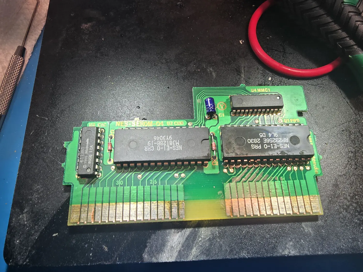
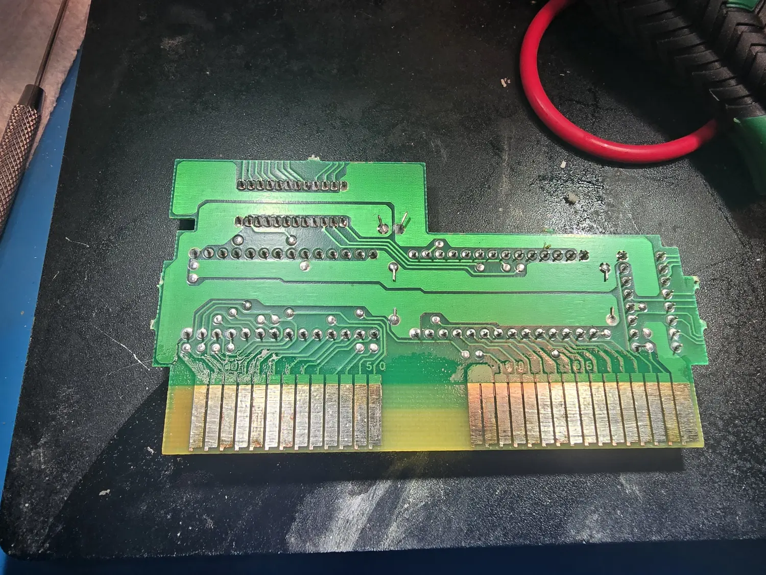
No power at all: dead, no light, no picture
Walk the power path in order rather than guessing. The NES-001 takes a 9 V AC adapter (the NES-002) into an onboard bridge rectifier, then a large reservoir capacitor produces a raw rail of roughly 12 to 13 V DC, which passes through the front-panel power switch and feeds a 7805 regulator that produces the 5.0 V DC the logic runs on. Check, in sequence:
- AC in at the jack (roughly 9 to 10 V AC unloaded).
- Raw DC across the reservoir cap (roughly 12 to 13 V DC).
- 5.0 V DC out of the 7805.
The usual culprits are corroded or cracked solder joints on the bridge rectifier in the metal power and RF module, a failed 7805, a dirty power switch, or a broken DC jack. One useful check: if all three pins of the 7805 read 0 V, the input never arrived (a short or open upstream), which points away from the regulator itself.
Two things worth knowing. First, the power LED is not a valid 5 V indicator on this console. Its circuit is tangled up with the reset and lockout logic, so the light can be dead with a perfectly good 5 V rail. Second, you can isolate the power and RF module: injecting a clean 5 V straight into the center pin of the mainboard power header (with ground) bypasses the whole module. If the console then plays, the fault is confined to that module.
Wavy or noisy video, hum bars, or a 60 Hz buzz
The usual suspect is the large 2200 uF reservoir capacitor on the AV and power module. Community references call it the single most common electrolytic failure on this console, affecting essentially every board revision. My own bench experience does not match that reputation: I have not yet had to replace one, whether because certain revisions were worse and I have not hit them or because I have been lucky. So I do not assume it. Check it: look for a bulged or leaking can and scope the raw rail for ripple, and replace it only if it is actually bad. It also sits inside the RF shielded module, which makes swapping it genuinely annoying, so it is not something to do on spec. But if a noisy picture or an audio buzz traces to a tired cap here, that is the one to replace.
Internal corrosion
Battery leaks and old liquid exposure leave corrosion, most often around the power and RF module joints and shielding. Left alone it spreads and eats traces. I neutralize active corrosion, clean thoroughly with isopropyl alcohol, and seal the treated area, the same process described in my restoration and testing writeup.
Inside the NES-001
A quick tour of what the hardware is actually doing, which makes the faults above make sense.
- Unlike the later top-loader (which is RF-only), the front-loader outputs stock composite video and mono audio on the rear RCA jacks in addition to RF. There is no “add composite” mod to do here; it is already there.
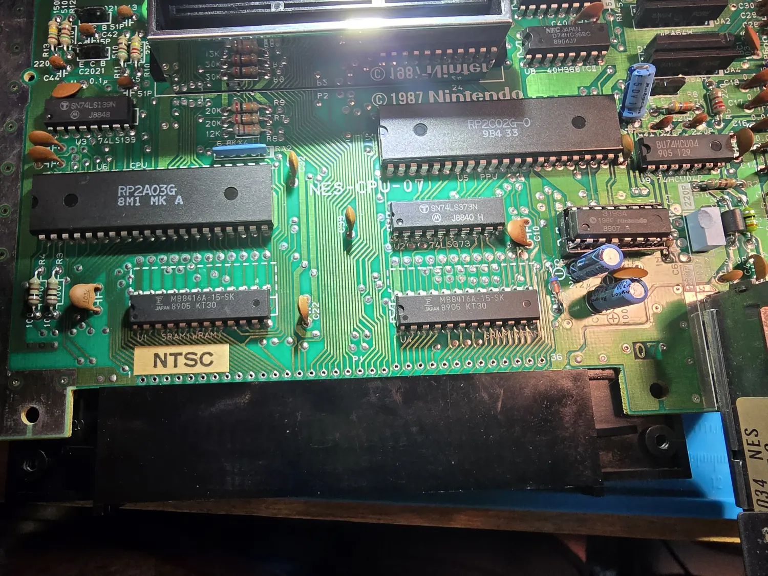
- The brains are two Ricoh chips: the RP2A03 CPU (a 6502 core plus the audio and controller logic) and the RP2C02 PPU, which generates the video. Around them sit two 2K SRAMs (work RAM and video RAM), a 74LS373 latch, a 74LS139 address decoder, a pair of 74HC368 buffers for the controller ports, a 74HCU04 that handles clock shaping and doubles as the audio amplifier stage, and the CIC lockout chip.
- Power: the 9 V AC adapter is a plain transformer. Because the console rectifies onboard with a full bridge, a DC supply of either polarity also powers it. The 7805 regulator sits on a modest heatsink, which matters if you ever add a power-hungry mod. The raw rail off the reservoir cap also feeds the analog side of the RF and modulator section.
- Two clocks run the machine: a 21.477272 MHz master oscillator and a separate 4 MHz clock for the lockout chip. A dead master oscillator takes the whole picture and sound out at once, which is a useful diagnostic split.
- The power and RF section is a separate shielded sub-board. Nintendo used two vendors for it, Alps and Mitsumi, and which one you have does not track the board revision. Identify it by the silkscreen when you recap, because the capacitor layout differs between them.
Mods worth knowing
This is an overview of what is worth doing and where to go for the real instructions, with one exception. The lockout disable gets written out in full in its own section below, because it is the one people ask me for and the version I use is not the version the published guides describe.
- Lockout (CIC) disable. The permanent cure for the region lock and the blink loop, and the mod I do most often. Three ways to do it, with full steps and the tradeoffs between them, are in Disabling the lockout chip below.
- 72-pin alternatives. Beyond refurbishing the original, the Blinking Light Win (Arcade Works) replaces the connector and tray so carts load flat with no push-down, and the Nin10-Drawer brings the top-loader-style connector into the NES-001. Both retire the pin-bend flaw by different means; supply on both is spotty. Reference: ConsoleMods: Blinking Light Win.
- RGB output: NESRGB. Tim Worthington’s board regenerates the video for RGB, S-video, and composite with no lag. It is an advanced install (a 40-pin PPU desolder and an auxiliary regulator). Reference: etim.net.au NESRGB.
- HDMI: Hi-Def NES. Kevtris’s kit reuses the console’s own CPU and PPU for a lag-free digital picture and audio. Advanced install, and it needs an E, G, or H revision CPU and PPU. Reference: game-tech Hi-Def NES.
- Digital scaler picture, low labor: Lumacode / PPUdigitizer. c0pperdragon’s board mounts under the PPU with no desolder and feeds a Lumacode-capable scaler. Reference: c0pperdragon PPUdigitizer.
- Expansion audio. A small resistor mod brings Famicom expansion audio (FDS, VRC6, and similar) from a flashcart to the console’s mixer, which the 72-pin slot otherwise cannot pass. Reference: ConsoleMods: Expansion Audio Mod.
- Replacement boards. When a board is beyond saving (acid damage, lifted traces), open-source and aftermarket motherboards such as OpenTendo, SM-Tendo, and the POW Block power module can turn it back into a working console with donor parts. Reference: OpenTendo.
For a broader mod orientation, RetroRGB’s NES mods index is the best single jumping-off page.
Disabling the lockout chip (CIC)
Disabling the console’s lockout chip retires the blinking-light reset loop for good and lets the machine boot unlicensed cartridges and cartridges from other regions. It is the mod I get asked about most, so this one I write out in full rather than pointing elsewhere.
Start with what it does not do. It is not a fix for a worn 72-pin connector. It stops the console complaining about a bad connection without improving the connection, and a game that runs on marginal contact can still corrupt the battery save on an SRAM cart. Service the connector first, then disable the lockout if you want to, not instead. It also will not make a PAL game run correctly on an NTSC console: region lock and video timing are two separate things, and the CPU, PPU and crystal decide the timing. My clones and PAL vs NTSC page covers what changes between regions.
Find the chip, and get its pin numbering right
The lockout chip is the 16-pin DIP sitting next to the metal RF and power box,
usually silkscreened U10. Its marking tells you the console’s region:
| Marking | Console region |
|---|---|
3193A | NTSC (North America and Japan) |
3195A | PAL-B, and Korea |
3196A | Asia and Hong Kong |
3197A | PAL-A |
The earliest boards carry a plain 3193 with no letter. Pin 1 is at the notched
end of the package, and the numbering runs down that side and back up the other,
so pin 4 is the fourth leg down from the notch on the pin-1 side.
One thing to unlearn before a probe goes anywhere near it: on this chip the supply is pin 16 and ground is pin 8. That is not the pin-14 and pin-7 arrangement of the 74-series logic sitting right next to it, and muscle memory will put you on a port pin.
Why pin 4 is the one everybody talks about
The console and the cartridge carry the same chip. Pin 4 is the strap that decides which role it plays: tied to +5 V it is the lock, which is how the console wires it, and tied to ground it is the key, which is how a cartridge wires it. Only a lock ever drives the reset line. So if you break pin 4’s connection inside the console, the chip’s internal pulldown reads the now floating pin as a 0, the console’s chip decides it is a key, and it stops resetting anything. Tying the disconnected pin to ground works too and is what most published guides tell you to do, but the internal pulldown makes that optional.
That is the whole trick. The first two methods below are just different ways of breaking that one connection, and what separates them is how reversible they are.
Method 1: socket the chip, then reinstall it with pin 4 outside the socket
This is the one I use, and it is what the photo below shows. Nothing on the board is cut, nothing on the chip is cut, and putting the console back to stock later takes about thirty seconds with no iron. The cost is that it is the most work up front, because it means desoldering a 16-pin DIP.
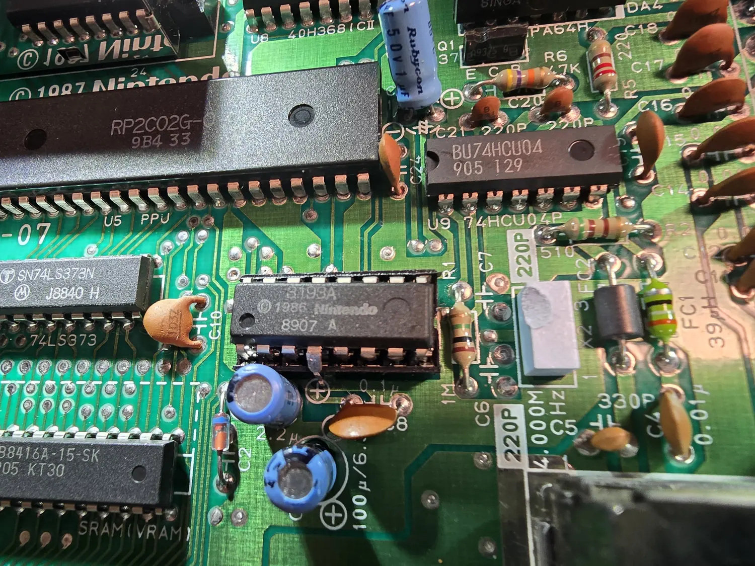
- Strip the console down to a bare board: top case off, RF shield off the mainboard, board out.
- Find the chip and photograph it in place. The notch and pin 1 have to go back the same way round, and once the chip is out, the silkscreen outline on the board is the only thing left telling you which way that was.
- Desolder the chip. This is the only step that carries real risk, so do it properly. Flux every joint, add fresh leaded solder to all 16 pins first so it mixes with the original and drops the melting point, then clear each hole with a desoldering gun or braid. Confirm all 16 legs move freely in their holes before you lift anything. Levering out a chip that is still held by one joint is how pads come off.
- Fit a 16-pin machined-pin (round-pin) DIP socket, notch matching the silkscreen. Do not use the cheap stamped dual-wipe kind. The entire point of this method is that the chip goes in and out cleanly for the rest of the console’s life, and stamped sockets do not grip reliably enough for that.
- Straighten the chip’s legs, then bend pin 4 outward to roughly 90 degrees so it stands clear of the package. Bend at the shoulder where the leg leaves the body, and do it in one movement. Working a leg back and forth at the same spot is what snaps it off.
- Seat the chip in the socket with the notch matching the silkscreen and pin 4 riding outside the socket instead of down into its hole. Check that the bent leg is not touching pin 3, pin 5, the socket body, or the RF shield once everything is back together.
- Reassemble and test with a cartridge you know is good, and with an out-of-region or unlicensed cart if you have one. You want a steady power light and a clean boot, with no blink.
Grounding the lifted pin is unnecessary. If you want to do it anyway, tack a short wire from the bent leg to any nearby ground.
To reverse it: pull the chip, straighten pin 4, seat it fully. The socket stays behind, which is an added part but not a change to the circuit.
Method 2: cut pin 4 in place
This is the version nearly every published guide describes, and it is the one I would skip. It works, and it takes ten minutes instead of an hour. Here is the procedure as ConsoleMods documents it:
- Strip the console down to a bare board as above.
- Cut the chip’s pin 4 with flush cutters, right at the board where the leg enters its solder joint.
- Bend the freed leg up to about 90 degrees, clear of the board.
- Solder a wire to the freed leg and sleeve the joint in heat shrink so it cannot short against a neighbour.
- Solder the other end of that wire to the nearest ground.
- Reassemble and test.
Two things to weigh before choosing it. It is only semi-reversible: going back to stock means soldering a now-shorter leg back onto its pad, on a chip nobody manufactures any more. And the lockout chip stays in the console’s reset path even with the lockout defeated, which is the part that bites people. A chip damaged while you are cutting at it does not just fail to disable, it takes the console’s reset with it, and the console will not boot at all. On this machine the power LED is wired into that same reset and lockout circuitry, so a dark power light is the usual way that shows up. If a console has already been left in exactly that state, the two-wire method below is the standard recovery.
You will also see people snip pin 4 off flush and leave it at that. Electrically it lands in the same place, since the internal pulldown does not care whether the pin is grounded or floating. It also throws the leg away, and with it any prospect of restoring the chip. ConsoleMods reaches the same verdict in fewer words: it works, but it is not recommended.
Method 3: the two-wire method
This one never touches pin 4. Instead it holds the lockout chip permanently in reset and hands its other job to the inverter next door, so the front-panel RESET button drives the CPU and PPU reset directly. Two wires, no cuts, and it is reversible by unsoldering them.
On an NES-001, with the 74HCU04 inverter usually silkscreened U9:
- Wire from the lockout chip’s pin 7, its own reset input, to pin 1 of the 74HCU04.
- Wire from pin 2 of the 74HCU04 to the lockout chip’s pin 9, the line that drives CPU and PPU reset.
The mechanism is worth understanding, because it explains why two wires and no cuts is enough. Pins 1 and 2 of that inverter are the gate running the 4 MHz oscillator that clocks the lockout chip. The first wire stops that oscillator, which is what holds the chip in reset and keeps it from ever asserting anything. The second repurposes the now-idle gate as a buffer, converting the reset button’s signal into the form the CPU and PPU expect. The lockout chip itself stays exactly where it is, in its solder joints, unmodified.
One documented side effect: some consoles then need a press of RESET after power-on before they will boot, because the CPU and PPU are no longer held in reset long enough at startup. The published fix is to replace C8 with a larger capacitor, 220 nF or more, which extends the power-on reset. That fix comes from a single source and I have not verified it on the bench.
If freehanding two wires onto adjacent DIP pins is not appealing, there is a small carrier PCB for the mod with gerbers published at OSH Park.
If the chip is already gone
Pulling the lockout chip and doing nothing else does not work. The console will not boot, because that chip is also the reset generator. There is a documented bypass that rebuilds the function with a resistor and a couple of wires on the empty footprint, meant for boards where the chip was destroyed or ripped out. It is salvage work, it rests on a single source, and on a board with a healthy chip any of the three methods above is a better answer. The procedure is on ConsoleMods.
What to expect afterwards, and the three carts that care
- Camerica, Color Dreams and Wisdom Tree cartridges. These defeated the
lockout in period by hitting it with a voltage spike from an onboard charge
pump. With the console’s chip disabled there is no load on the far end of that
circuit, and the carts have been reported to overheat. Later boards
(
NES-CPU-11, 1990 onward) carry series resistors and clamp diodes on the lockout data lines, though not on the reset lines. - Nintendo World Championships 1990. These need the cartridge-reset signal that a working lock generates, and will not run against a disabled one. Unlikely to ever matter, and worth knowing if you own one.
- Out-of-region carts. They will boot, which is the point. A PAL game on an NTSC console still runs too fast with its music too sharp, and effects the game times by counting CPU cycles can land on the wrong line, because the CPU, PPU and crystal decide that and none of them has changed. The colours come from the console’s PPU, so they are ordinary NTSC colours. The details are on my clones and PAL vs NTSC page.
Recap and parts
Most of the recap fear around the NES-001 is misplaced. The main board carries only three electrolytic capacitors, and they rarely fail. Community references single out the 2200 uF reservoir capacitor on the AV and power module as the failure magnet. My own bench experience does not match that: I have not had to replace one yet, whether because certain revisions were worse and I have not hit them or because I have simply been lucky. So my rule is inspect, do not assume: check that 2200 uF for bulging or leaking, replace it only if it is actually bad, and recap the rest of the module only where a cap reads bad or a fault points at it. Because that cap sits inside the RF shielded module, replacing it is a real chore, which is one more reason not to pull it on spec.
A few practical notes:
- Match the module before you order. The Alps and Mitsumi modules use different capacitor designators and values, so identify yours by the silkscreen. Vendors sell a complete NES-001 cap kit that covers the common cases, which is the low-effort path.
- Desolder the module from the module side. When pulling the power and RF module, desolder its pins from the module PCB, not from the mainboard, because the mainboard traces to those pins are top-side only and their vias dislodge easily.
- 7805 regulator. If it is dead or regulating high, any reputable 78xx-family 5 V TO-220 part (for example an L7805CV) drops in. Keep the heatsink.
- Some parts are effectively unobtainium new. The Japanese discrete transistors (the 2SA937 video buffer and the 2SC2021 oscillator pair) and the original diode arrays are new-old-stock or donor-board only. On a fleet, the worst board is your parts stock.
If you would rather buy a console that has already had this work done, or you need a tested cartridge to go with it, everything I restore is in the shop. (I will link specific NES service and recap-related listings here as those pages firm up.)
The hard data behind all of the above (the per-module cap maps with substitutes, the non-cap parts a repair consumes, the chip and connector pinouts, and the schematic facts I probe against) is tabled in the sections that follow. Long per-item notes fold away to keep it readable; expand any of them for the full detail.
Capacitor lists
The main board carries three electrolytics on the late revisions; everything else worth checking is on the power and RF module, and those maps are per-variant. Match your module by its silkscreen before you order, because the vendor board does not track the NES-CPU number.
NES-CPU-01..03 NES-CPU-01 / -02 / -03 (1985-86, NYC and early test market)
Board p/n: NES-CPU-01 · NES-CPU-02 · NES-CPU-03
Main board — electrolytics
| Desig | Value | V | OEM p/n | Substitute | Note |
|---|---|---|---|---|---|
| C1 | 100µF | 6.3V | — | Panasonic ECE-A0JKA101I or any 100µF ≥6.3V radial (5x7 mm) | 7805 output decoupling ✓console5,opentendo |
notes on C1The main board carries only these three electrolytics; everything else on it is ceramic and does not age out. Voltage ratings here are minimums: going up is always fine and usually easier to source. Confirmed directly against the OpenTendo reverse-engineered schematic for this revision, which agrees with the Console5 list on all three designators and values. | |||||
| C9 | 2.2µF | 50V | — | Panasonic ECA-1HHG2R2I or any 2.2µF ≥50V radial (5x11 mm) | ✓console5,opentendo |
| C23 | 1µF | 50V | — | Nichicon UVR2A010MDD1TD (a 100V part; higher voltage is fine) | ✓console5,opentendo |
NES-CPU-04 NES-CPU-04 (1986-87; first PAL board)
Board p/n: NES-CPU-04
Main board — electrolytics
| Desig | Value | V | OEM p/n | Substitute | Note |
|---|---|---|---|---|---|
| C1 | 100µF | 6.3V | — | Panasonic ECE-A0JKA101I or any 100µF ≥6.3V radial (5x7 mm) | 7805 output decoupling ✓console5,opentendo |
notes on C1The main board carries only these three electrolytics; everything else on it is ceramic and does not age out. Voltage ratings here are minimums: going up is always fine and usually easier to source. Confirmed directly against the OpenTendo reverse-engineered schematic for this revision, which agrees with the Console5 list on all three designators and values. | |||||
| C9 | 2.2µF | 50V | — | Panasonic ECA-1HHG2R2I or any 2.2µF ≥50V radial (5x11 mm) | ✓console5,opentendo |
| C23 | 1µF | 50V | — | Nichicon UVR2A010MDD1TD (a 100V part; higher voltage is fine) | ✓console5,opentendo |
NES-CPU-05..08 NES-CPU-05 / -06 / -07 / -08 (1987-90; final video configuration, G-die CPU and PPU)
Board p/n: NES-CPU-05 · NES-CPU-06 · NES-CPU-07 · NES-CPU-08
Main board — electrolytics
| Desig | Value | V | OEM p/n | Substitute | Note |
|---|---|---|---|---|---|
| C1 | 100µF | 6.3V | — | Panasonic ECE-A0JKA101I or any 100µF ≥6.3V radial (5x7 mm) | 7805 output decoupling benchconsole5,opentendo,consolemods,mem-bench |
notes on C1The main board carries only these three electrolytics; everything else on it is ceramic and does not age out. Voltage ratings here are minimums: going up is always fine and usually easier to source. Confirmed on my own bench on a NES-CPU-07 board: Nintendo silkscreened the values next to the pads on this revision, and the board reads “100µ/6.3” and “2.2µ” at the two positions below, with the third electrolytic a Rubycon marked 50V 1µF. That is first-hand agreement with the Console5 list, which gives one main-board list for every NES-001 revision with no per-revision split. Consistent with the schematics either side of this group (the identical three caps appear on the -04 sheet below it and the -10 and -11 boards above it), and with the fact that the documented changes at these revisions are resistors and diodes (the video-amp collector resistor, the CIC clock and clamp parts), none of which touch an electrolytic. | |||||
| C9 | 2.2µF | 50V | — | Panasonic ECA-1HHG2R2I or any 2.2µF ≥50V radial (5x11 mm) | benchconsole5,opentendo,mem-bench |
notes on C9Silkscreened “2.2µ” on the NES-CPU-07 board on my bench. | |||||
| C23 | 1µF | 50V | — | Nichicon UVR2A010MDD1TD (a 100V part; higher voltage is fine) | benchconsole5,opentendo,mem-bench |
notes on C23Fitted as a Rubycon 50V 1µF on the NES-CPU-07 board on my bench. | |||||
NES-CPU-09 NES-CPU-09 (1989-90; CIC anti-tamper hardening begins)
Board p/n: NES-CPU-09
Main board — electrolytics
| Desig | Value | V | OEM p/n | Substitute | Note |
|---|---|---|---|---|---|
| C1 | 100µF | 6.3V | — | Panasonic ECE-A0JKA101I or any 100µF ≥6.3V radial (5x7 mm) | 7805 output decoupling ✓console5,opentendo,consolemods |
notes on C1The main board carries only these three electrolytics; everything else on it is ceramic and does not age out. Voltage ratings here are minimums: going up is always fine and usually easier to source. No OpenTendo schematic exists for this revision specifically, so this list is Console5’s (which gives one main-board list for every NES-001 revision, with no per-revision split) carried across. It is well bracketed: I confirmed the identical three caps on the -04 schematic below this revision and on the -10 and -11 boards above it, and the documented changes at this revision are resistors and diodes (the video-amp collector resistor and the CIC clock and clamp parts), none of which touch an electrolytic. | |||||
| C9 | 2.2µF | 50V | — | Panasonic ECA-1HHG2R2I or any 2.2µF ≥50V radial (5x11 mm) | ✓console5,opentendo |
| C23 | 1µF | 50V | — | Nichicon UVR2A010MDD1TD (a 100V part; higher voltage is fine) | ✓console5,opentendo |
NES-CPU-10 NES-CPU-10 (about 1990; second CIC series resistor, some boards with factory-added clamp diodes)
Board p/n: NES-CPU-10
Main board — electrolytics
| Desig | Value | V | OEM p/n | Substitute | Note |
|---|---|---|---|---|---|
| C1 | 100µF | 6.3V | — | Panasonic ECE-A0JKA101I or any 100µF ≥6.3V radial (5x7 mm) | 7805 output decoupling: the one main-board electrolytic worth checking on a brown-out ✓console5,opentendo,edc-pwr |
notes on C1Voltage ratings on this board are minimums. Going up is always
fine and usually easier to source. | |||||
| C9 | 2.2µF | 50V | — | Panasonic ECA-1HHG2R2I or any 2.2µF ≥50V radial (5x11 mm) | ✓console5,opentendo |
| C23 | 1µF | 50V | — | Nichicon UVR2A010MDD1TD (a 100V part; higher voltage is fine) | ✓console5,opentendo |
NES-CPU-11 NES-CPU-11 (1990-93; final revision, full CIC stun and -5V hardening)
Board p/n: NES-CPU-11
Main board — electrolytics
| Desig | Value | V | OEM p/n | Substitute | Note |
|---|---|---|---|---|---|
| C1 | 100µF | 6.3V | — | Panasonic ECE-A0JKA101I or any 100µF ≥6.3V radial (5x7 mm) | 7805 output decoupling ✓console5,opentendo,edc-pwr |
| C9 | 2.2µF | 50V | — | Panasonic ECA-1HHG2R2I or any 2.2µF ≥50V radial (5x11 mm) | ✓console5,opentendo |
| C23 | 1µF | 50V | — | Nichicon UVR2A010MDD1TD (a 100V part; higher voltage is fine) | ✓console5,opentendo |
NESE-001 NESE-001 (PAL build of the NES-CPU-04 and later boards)
Board p/n: NES-CPU-04 and later, PAL parts fitted
Main board (PAL parts) — electrolytics
| Desig | Value | V | OEM p/n | Substitute | Note |
|---|---|---|---|---|---|
| C1 | 100µF | 6.3V | — | Panasonic ECE-A0JKA101I or any 100µF ≥6.3V radial (5x7 mm) | 7805 output decoupling ✓console5,consolemods,opentendo |
notes on C1The PAL machine uses the same main-board designs as the NTSC one, so the same three electrolytics apply. Nintendo did not lay out region-specific boards; only the CPU, PPU, clock crystal and lockout chip change between regions. The PAL-specific capacitors are on the RF and power module, not here: see the RF-MOD entry for the Alps FR853 list, which carries a PAL-only C1 10µF/16V and the 10nF ceramic at C34 that has been reported burned on multiple PAL units. One exception to watch: French NES consoles have no RF modulator at all. They carry a rear RGB connector instead, so the module list does not apply to them even though this main-board list does. | |||||
| C9 | 2.2µF | 50V | — | Panasonic ECA-1HHG2R2I or any 2.2µF ≥50V radial (5x11 mm) | ✓console5,opentendo |
| C23 | 1µF | 50V | — | Nichicon UVR2A010MDD1TD (a 100V part; higher voltage is fine) | ✓console5,opentendo |
RF-MOD Power / RF modulator sub-board variants (fitted across all NES-CPU revisions)
Board p/n: Alps and Mitsumi, several layouts: identify by silkscreen, NOT by NES-CPU revision
Alps, brown PCB, BA20-type bridge (revised) — electrolytics
| Desig | Value | V | OEM p/n | Substitute | Note |
|---|---|---|---|---|---|
| C21 | 2200µF | 25V | — | Nichicon UVZ1E222MHD (12.5 mm dia, 5 mm lead spacing): check the can against your module | the reservoir cap; Console5 and ConsoleMods call it the failure magnet, my bench does not agree: see the notes ✓console5,consolemods,mem-bench |
notes on C21Console5 and ConsoleMods both single this cap out: ConsoleMods describes it as especially failure-prone, causing excessive interference and noise in the video signal, across practically all board revisions. That is what those sources say. My bench does not agree. Across the units I have gone through I have not yet had to replace one. I cannot tell you why the gap exists: it could be that certain revisions really are worse and I have not hit them, or it could be sample luck. Either way I do not assume it. So my rule is inspect, do not assume. Look for a bulged or leaking can, scope the raw rail for ripple, and replace it only if it is actually bad or a hum-bar or video-noise fault traces to it. It lives inside the RF shielded module, which makes it a genuinely annoying part to swap, so it is not a job to do on spec. The schematic draws this as a 15 V part and Console5’s replacement spec is 25 V. Use the 25 V. | |||||
| C1 | 10µF | 35V | — | 10µF ≥25V radial (25V is fine here) | single sourceconsole5 |
| C23 | 10µF | 35V | — | 10µF ≥25V radial | single sourceconsole5 |
| C25 | 100µF | 10V | — | 100µF ≥16V radial | single sourceconsole5 |
| C29 | 1µF | 50V | — | 1µF ≥50V radial | single sourceconsole5 |
Alps, green PCB with floating cap, BA20-type bridge — electrolytics
| Desig | Value | V | OEM p/n | Substitute | Note |
|---|---|---|---|---|---|
| C30 | 2200µF | 25V | — | Nichicon UVZ1E222MHD: check the can diameter and lead spacing | reservoir cap on this layout; see the failure-claim note on the brown-PCB C21 row single sourceconsole5,consolemods |
notes on C30Same cap, different designator. Console5 and ConsoleMods call it
the failure magnet; my bench has not agreed so far, so I inspect
rather than replace on spec. | |||||
| C19 | 1µF | 50V | — | 1µF ≥50V radial | single sourceconsole5 |
| C33 | 1µF | 50V | — | 1µF ≥50V radial | single sourceconsole5 |
| C34 | 100µF | 6.3V | — | 100µF ≥16V radial | single sourceconsole5 |
| unlabelled | 1µF | 50V | — | anything 1-100µF at ≥16V is acceptable here | no silkscreen designator: it sits across the regulator input and ground single sourceconsole5 |
notes on unlabelledThere is no dedicated cap-map image for this layout, so locate
this one by following the regulator input pin. | |||||
Alps FR853, four discrete diodes — electrolytics
| Desig | Value | V | OEM p/n | Substitute | Note |
|---|---|---|---|---|---|
| C21 | 2200µF | 25V | — | Nichicon UVZ1E222MHD: check the can against your module | reservoir cap; see the failure-claim note on the brown-PCB C21 row single sourceconsole5,consolemods |
| C1 | 10µF | 16V | — | 10µF ≥16V radial | PAL boards only single sourceconsole5 |
| C23 | 100µF | 25V | — | 100µF ≥25V radial | single sourceconsole5 |
| C25 | 100µF | 10V | — | 100µF ≥16V radial | single sourceconsole5 |
| C29 | 1µF | 50V | — | 1µF ≥50V radial | single sourceconsole5 |
| C34 | 10nF | — | — | 0.01µF ≥50V ceramic | ceramic, not an electrolytic: listed because burned C34 discs have been reported on PAL FR853 boards single sourceconsole5 |
notes on C34This one is here for a specific reason: multiple PAL FR853 boards
have turned up with this 10 nF ceramic disc burned. If you are
working a PAL module, look at it. | |||||
| C35 | 1µF | 50V | — | 1µF ≥50V radial | single sourceconsole5 |
| C36 | 10µF | 16V | — | 10µF ≥16V radial | single sourceconsole5 |
Alps SH-SH5 / FS074, four discrete diodes — electrolytics
| Desig | Value | V | OEM p/n | Substitute | Note |
|---|---|---|---|---|---|
| C21 | 2200µF | 25V | — | Nichicon UVZ1E222MHD: check the can against your module | reservoir cap; see the failure-claim note on the brown-PCB C21 row single sourceconsole5,consolemods |
| C23 | 100µF | 25V | — | 100µF ≥25V radial | single sourceconsole5 |
| C25 | 100µF | 10V | — | 100µF ≥16V radial | single sourceconsole5 |
| C29 | 1µF | 50V | — | 1µF ≥50V radial | single sourceconsole5 |
| C36 | 10µF | 16V | — | 10µF ≥16V radial | single sourceconsole5 |
| C37 | 1µF | 50V | — | 1µF ≥50V radial | same layout family as FR853 but with several caps re-oriented: check polarity against the board, not against the FR853 map single sourceconsole5 |
Mitsumi TDK-T12V — electrolytics
| Desig | Value | V | OEM p/n | Substitute | Note |
|---|---|---|---|---|---|
| C26 | 2200µF | 25V | — | Nichicon UVZ1E222MHD: check the can against your module | reservoir cap on this layout; see the failure-claim note on the brown-PCB C21 row single sourceconsole5,consolemods |
| C2 | 10µF | 16V | — | 10µF ≥16V radial | single sourceconsole5 |
| C6 | 10µF | 16V | — | 10µF ≥16V radial | single sourceconsole5 |
| C29 | 100µF | 16V | — | 100µF ≥16V radial | single sourceconsole5 |
| C31 | 100µF | 25V | — | 100µF ≥25V radial | single sourceconsole5 |
| C32 | 10µF | 16V | — | 10µF ≥16V radial | single sourceconsole5 |
Mitsumi TDK-T31V — electrolytics
| Desig | Value | V | OEM p/n | Substitute | Note |
|---|---|---|---|---|---|
| C21 | 2200µF | 25V | — | Nichicon UVZ1E222MHD: check the can against your module | reservoir cap; see the failure-claim note on the brown-PCB C21 row single sourceconsole5,consolemods |
notes on C21A sub-variant of the T31V exists with a ferrite choke between the
DC jack and the bridge and shifted cap numbers. If your board has
that choke, verify every designator against the physical board
before ordering. | |||||
| C6 | 10µF | 16V | — | 10µF ≥16V radial | single sourceconsole5 |
| C22 | 100µF | 16V | — | 100µF ≥16V radial | single sourceconsole5 |
| C25 | 100µF | 10V | — | 100µF ≥16V radial | single sourceconsole5 |
Mitsumi MTM-8V-0 / VIX — electrolytics
| Desig | Value | V | OEM p/n | Substitute | Note |
|---|---|---|---|---|---|
| C20 | 2200µF | 25V | — | Nichicon UVZ1E222MHD: check the can against your module | reservoir cap on this layout; see the failure-claim note on the brown-PCB C21 row single sourceconsole5,consolemods |
notes on C20No cap-map image exists for this layout, so locate the designators
on the silkscreen. | |||||
| C5 | 10µF | 35V | — | 10µF ≥25V radial (25V is fine here) | single sourceconsole5 |
| C21 | 100µF | 16V | — | 100µF ≥16V radial | single sourceconsole5 |
| C24 | 100µF | 10V | — | 100µF ≥16V radial | single sourceconsole5 |
Replacement parts
The non-cap parts an NES-001 repair actually goes through, including the several that are donor-board-only now.
Non-cap consumables
| Function | OEM part | Why replaced | Substitute | Note |
|---|---|---|---|---|
| 72-pin cartridge connector | Nintendo 72-pin ZIF connector (no new OEM production) | contact corrosion and pins permanently bent down by years of push-down insertions: the number-one fault on this console | refurbish the original (boil and re-tension); generic aftermarket about $13; Blinking Light Win or Nin10-Drawer to retire the flaw entirely | I refurbish the original rather than fit a generic clone ✓consolemods,mem-bench |
notesConsoleMods puts it plainly: replacement 72-pin connectors are either hard to find or of very low quality and will have the same or worse issues than a worn OEM connector. That matches what I see, so a refurbished original is my default on anything resale-grade. Refurbish method: submerge the connector pins-down in boiling water for about 30 minutes, let it cool, rinse with isopropyl alcohol, and dry it fully before refitting. The shape-memory of the metal pulls the bent pins back up. Do not sand, Brasso or magic-eraser the pins: that strips the plating and makes the contact permanently worse. Two permanent fixes exist if you want the design flaw gone rather than reset: the Blinking Light Win loads carts horizontally on a card edge with no push-down, and the Nin10-Drawer brings the top-loader-style connector into the NES-001. Both retire the downward-wipe wear; only the cheap generic clones reproduce it. Supply on both is chronically spotty. | ||||
| 2200µF reservoir capacitor (power / RF module) | 2200µF, drawn as 15V on the schematic; Console5 specifies 25V for replacement | sources call it the near-universal failure; my bench has not agreed: inspect, do not assume | Nichicon UVZ1E222MHD (2200µF 25V, 12.5 mm dia, 5 mm lead spacing) | inside the RF shielded module, so it is a real chore to reach ✓console5,consolemods,mem-bench |
notesConsole5 and ConsoleMods both treat this as the cap to replace on every NES-001; ConsoleMods attributes video noise and interference to it across practically all board revisions. That is their position, and it is worth knowing. Mine is different. I have not yet had to replace one. Whether that is because the failures cluster on revisions I have not seen enough of, or because I have had a lucky sample, I genuinely cannot say. So I inspect for a bulged or leaking can and scope the raw rail for ripple, and I replace it when it is actually bad: not on principle. Check the can diameter and lead spacing against your specific module before buying in bulk; the variants differ. | ||||
| +5V regulator | AN7805 (one recorded example; units shipped with various 78xx brands) | dead or regulating high | STMicro L7805CV, or any reputable 78xx-family 5V TO-220 (onsemi MC7805CTG, TI UA7805) | keep the heatsink ✓console5,mem-bench |
notesBefore condemning it: if all three terminals read 0 V the input never
arrived, which is a short or an open upstream, not a bad regulator. | ||||
| Master crystal | 21.477272 MHz crystal (X1) | cracked or drifting takes picture and sound out together | ECS ECS-214-S-4X | a dead master oscillator kills video and audio at once: a useful diagnostic split ✓opentendo,edc-cpu |
notesThe oscillator is discrete: the crystal plus two 2SC2021 transistors (Q2
and Q3) as oscillator and buffer. If the picture and the sound are both
gone but the 5 V rail is good, look here before you look at the CPU. | ||||
| CIC clock resonator | 4 MHz ceramic resonator, marked "4000A" (X2) | dead resonator means the lockout handshake never completes: constant reset, and often no power light | Murata CSTLS4M00G56-B0 | ✓opentendo,edc-cpu,noa |
| Composite video buffer transistor | ROHM 2SA937 PNP (Q1) | video present at PPU pin 21 but nothing at the RCA jack | no verified modern drop-in; NOS, reclaimed, or donor board. A 2N3906 is the commonly cited stand-in but its pinout differs | out of franchised distribution ✓opentendo,nesdev-ppu |
notesThe OpenTendo BOM lists this with no distributor part at all. A generic
small-signal PNP probably works in this low-demand position, but nothing
in my sources confirms it, so validate video quality on a bench unit
before you standardise on a substitute across a fleet. | ||||
| Master oscillator transistors | ROHM 2SC2021 x2 (Q2, Q3) | dead 21 MHz oscillator | no verified modern drop-in; NOS, reclaimed, or donor board | out of franchised distribution ✓opentendo |
| Controller-port diode arrays | ROHM DAN601 (DA1-DA4) | port faults: Nintendo's own fault chain lists these after the 368 buffers and the CPU | no verified through-hole drop-in; NOS, reclaimed, or donor board | out of franchised distribution ✓opentendo,noa |
| Work / nametable SRAM | 2K x 8 DIP-24 SRAM (U1, U4) | bad work RAM or bad nametable RAM | Renesas 6116SA15SOG (SOIC) on a SOIC-24-to-DIP-24 adapter, or pull from a donor board | DIP-24 6116-class SRAM is effectively gone from franchised distribution ✓opentendo,console5 |
notesBoards up to NES-CPU-05 take narrow DIP only; NES-CPU-06 and later accept
either width. On a fleet, a donor board is usually faster than an adapter
stack. | ||||
| Audio-amp / clock inverter | 74HCU04 (U9): UNBUFFERED | no audio, distorted audio, or an oscillating audio stage after a wrong substitution | TI SN74HCU04N. Do NOT fit a buffered HC04, HCT04 or LS04 | the single most common wrong substitution on this board ✓opentendo,console5 |
notesOne gate of this chip is biased as a linear inverting amplifier with 47k
of feedback. A buffered part has three cascaded stages instead of one, so
it has far too much open-loop gain and phase shift and will oscillate or
distort. The DC bias still looks right, which is what makes this a trap. | ||||
| CIC data-line clamp zeners | 5.1V zener x2 (D2, D3 on NES-CPU-11) | restoring the late-revision CIC protection, or repairing a board that saw a stun circuit | onsemi 1N5231B | paired with two 1k series resistors (R18, R19) on the CIC data lines ✓opentendo,consolemods |
| Replacement lockout chip | 3193A (donor board only) | dead CIC, or a region-free build that keeps normal reset behaviour | NullCIC (open-source drop-in), krikzz AVR ATtiny13A CIC, or Kevtris CIClone | for a plain lockout disable you need no parts at all: lift pin 4 ✓consolemods,nesdev-cicpin |
notesThe pin-4 method is free and reversible if you lift rather than cut. Watch
the power LED: the CIC circuit is entangled with the LED and reset path,
so a simple pin-4 cut can kill the light. On anything I care about I use
the two-wire method that reroutes the reset button through the glue logic
instead. | ||||
| Power / Reset switch assembly | front-panel Power/Reset switch assembly | dirty or failed contacts: the power switch interrupts the RAW rail, not the 5V output | clean first; no new production found, so donor board otherwise | on Nintendo's own fault tables for both no-operation and no-power-light ✓noa,edc-pwr |
Inside the controller
The NES pad is the most repairable controller of its generation, and the reason is the shift register: it is a plain CD4021B, an 8-bit parallel-in / serial-out jellybean that is still in production. A dead one is a part you order, not a donor you hunt. Compare the SNES, whose pad uses Nintendo house shift registers with no substitute at all.
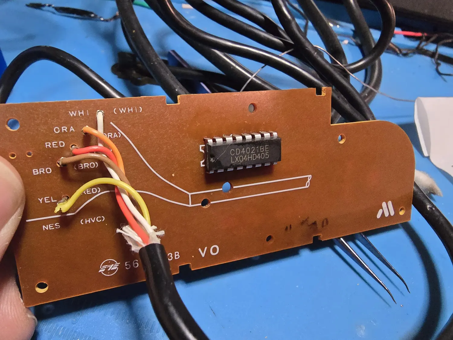
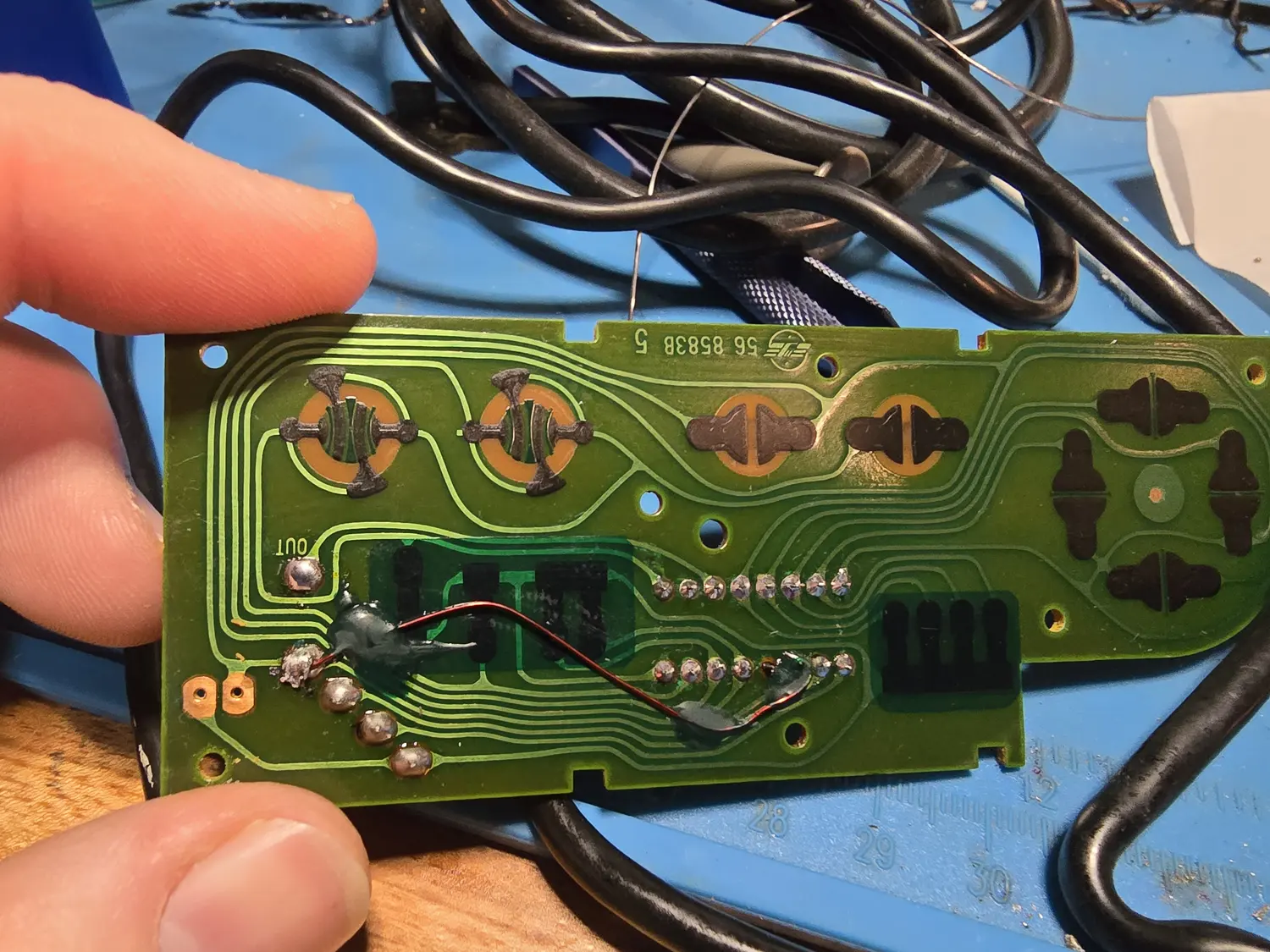
Eight buttons sit on the eight parallel inputs and shift out of Q8. The inputs are held high by a 45 kΩ × 8 resistor network and pulled down by the carbon contact pads, so a pad that reports a button stuck ON is usually a contact or a pull-up problem rather than a dead chip.
One detail that trips people mid-repair: some pads fit a 3.6 kΩ resistor on the OUT0 latch line and some do not. The OEM drawing annotates it as “not present in all models,” so its absence is not a fault and does not need correcting.
Before suspecting the electronics at all, check the cable. The overwhelming majority of dead or intermittent NES pads are a broken conductor at the strain relief, and the five-way header inside the shell is where you land a replacement.
Pin tables for the CD4021 and the internal header are in the component library below. For how this compares with the SNES, Genesis and N64 pads (and why the choice of shift register decides whether a dead pad is repairable), see Controllers: How Five Consoles Read a Button.
Chip & connector pinouts
Each IC and connector is defined once, with an interactive pin diagram and a folded pin table. The 72-pin cartridge edge and the underside expansion port are the two I reach for most.
Components & pinouts
Each part is defined once. The revision badge on every card shows exactly which board revision(s) it applies to.
Every diagram rotates and flips to match the board in front of you, zooms from a whole-package overview up to 3.2×, and saves at the orientation you are looking at — ↓ SVG matches the screen, and ↓ SVG (print) gives you the same drawing as ink on white. Both are vector, so print them at any size you like, which is the better route for the long connector pinouts since printing this page has to shrink them to fit the sheet. The # beside a part name links to that card, and the one in the pin panel links to a single pin — either link opens the card for whoever you send it to.
Hex inverting three-state buffer (controller reads) 74HC368N / PC74HC368P (U7, U8) NES-CPU-01..03 · NES-CPU-04 · NES-CPU-05..08 · NES-CPU-09 · NES-CPU-10 · NES-CPU-11 · NESE-001 dip-16✓philips-hc368,nexperia-hc368,edc-cpu,console5,opentendo#
U7 and U8: gate the controllers' serial data onto the CPU bus at $4016 and $4017
Dead or stuck buttons on one port, with the other port fine, is the pattern that sends me here. Nintendo’s port-fault chain is these buffers, the CPU, the DA1-DA4 diode arrays, and the RA1/RA2 resistor arrays, in that order.
Pin data is the Philips 74HC/HCT368 product specification, which is the lineage the PC74HC368P marking comes from, cross-checked against Nexperia’s current rev 5 sheet for the same part. The EDC schematic lists U7 and U8 as 74HC368 with power on 16 and ground on 8, which agrees.
Read the package as six inverting three-state buffers split into a group of four (enabled by pin 1) and a group of two (enabled by pin 15), which is the odd bit of the ‘368: it is not a clean 3+3 split. Both enables are active low. Note the outputs INVERT: the controller data arriving at an A pin comes out of the matching Y pin flipped, which is exactly what you want when the pad’s switches pull to ground.
Marking to expect on the board: OpenTendo draws U7 and U8 as “40H368”, which is the Nintendo house number. The EDC sheet calls the same positions 74HC368. Same part.
Click a pin to see its signal, net, and sources.
Interactive diagram needs JavaScript. The full pinout is in the table below.
| Pin | Signal | Cat | Net | Note |
|---|---|---|---|---|
| 1 | /1OE | signal | oe_a | output enable for buffers 1-4, active low ✓ |
| 2 | 1A | signal | in1 | data input ✓ |
| 3 | 1Y | signal | out1 | inverted three-state output onto the CPU data bus ✓ |
| 4 | 2A | signal | in2 | data input ✓ |
| 5 | 2Y | signal | out2 | inverted three-state output ✓ |
| 6 | 3A | signal | in3 | data input ✓ |
| 7 | 3Y | signal | out3 | inverted three-state output ✓ |
| 8 | GND | gnd | gnd | ✓ |
| 9 | 4Y | signal | out4 | inverted three-state output ✓ |
| 10 | 4A | signal | in4 | data input ✓ |
| 11 | 5Y | signal | out5 | inverted three-state output: this half is enabled by pin 15, not pin 1 ✓ |
| 12 | 5A | signal | in5 | data input ✓ |
| 13 | 6Y | signal | out6 | inverted three-state output ✓ |
| 14 | 6A | signal | in6 | data input ✓ |
| 15 | /2OE | signal | oe_b | output enable for buffers 5 and 6 only, active low: the '368 splits 4 + 2, not 3 + 3 ✓ |
| 16 | +5V | rail | vcc | ✓ |
CIC lockout chip (10NES) Nintendo 3193A (plain 3193 on the earliest boards); PAL-A 3197, PAL-B 3195, Asia 3196 NES-CPU-01..03 · NES-CPU-04 · NES-CPU-05..08 · NES-CPU-09 · NES-CPU-10 · NES-CPU-11 · NESE-001 dip-16✓nesdev-cicpin,nesdev-cic,edc-cpu,opentendo#
U10: a 4-bit microcontroller; pin 4 sets the lock/key role (high = lock, the console side) and Vcc is pin 16, not pin 14
Console and cartridge carry the same die. Pin 4 decides which one it is: pulled to +5V it is the lock (the console), grounded it is the key (the cart). That is the whole basis of the pin-4 disable mod: lift pin 4 and the console’s CIC stops behaving as a lock, and the internal pulldown reads the floating pin as a key.
The handshake runs over cart edge pins 34 and 35 with both chips clocked from the shared 4 MHz oscillator on pin 6 (cart edge pin 71); the lock resets the cart’s key through its pin 10 and cart edge pin 70. When the handshake fails, the lock pulses /host reset (pin 9) at about 1 Hz: the famous blink. In practice that is nearly always a dirty or bent 72-pin connector, not a dead CIC.
Two cautions. First, Vcc is pin 16 and ground is pin 8, so this is not the pin-14/pin-7 layout your muscle memory expects from 74-series logic. Second, the CIC circuit is tangled up with the power LED and reset path, so a chip damaged while cutting pin 4 leaves a console that will not boot and a power LED that never lights. The socketed pin-4 lift and the two-wire method both avoid cutting anything; see the page’s “Disabling the lockout chip” section.
Pins 1, 2, 3, 4, 6, 9 and 10 are corroborated by the OpenTendo CPU-11 sheet and the EDC schematic. The remaining port pins come from the NESdev pinout alone.
Click a pin to see its signal, net, and sources.
Interactive diagram needs JavaScript. The full pinout is in the table below.
| Pin | Signal | Cat | Net | Note |
|---|---|---|---|---|
| 1 | Data Out | signal | cic_dout | P0.0: console-to-cart data; reaches the key on cart edge pin 35 ✓ |
| 2 | Data In | signal | cic_din | P0.1: cart-to-console data; cart edge pin 34 ✓ |
| 3 | Seed | signal | cic_seed | P0.2: seed select ✓ |
| 4 | Lock/Key | signal | cic_role | P0.3: high = lock (console), low = key (cart). This is the pin the disable mod lifts ✓ |
| 5 | Xout | nc | clock output, unused here single source | |
| 6 | Xin / CLK | signal | cic_clk | 4.000 MHz clock in from the resonator; shared with the cart key via edge pin 71 ✓ |
| 7 | Reset | signal | cic_rst | the lock's own reset input, off the system reset bus ✓ |
| 8 | GND | gnd | gnd | ground is pin 8, not pin 7: this is not a 74-series layout ✓ |
| 9 | /Host reset | signal | reset | P1.0: pulses at about 1 Hz when the handshake fails; that is the blink ✓ |
| 10 | Slave reset | signal | cic_slave_rst | P1.1: resets the cartridge key via cart edge pin 70 ✓ |
| 11 | Speed A | signal | gnd | P1.2: grounded / reset-speed strap single source |
| 12 | Speed B | signal | gnd | P1.3: grounded / reset-speed strap single source |
| 13 | GND | gnd | gnd | P2.0: tied to ground single source |
| 14 | GND | gnd | gnd | P2.1: tied to ground (NOT Vcc; the supply is pin 16) single source |
| 15 | GND | gnd | gnd | P2.2: tied to ground single source |
| 16 | +5V | rail | vcc | supply: pin 16, the corner opposite ground ✓ |
72-pin cartridge connector 72-pin ZIF card edge, 2.50 mm pitch (NOT 0.1 inch) NES-CPU-01..03 · NES-CPU-04 · NES-CPU-05..08 · NES-CPU-09 · NES-CPU-10 · NES-CPU-11 · NESE-001 edge-72✓nesdev-cart,edc-cpu,console5#
the signature part of this console and its number-one fault; carries two independent buses (CPU and PPU) plus the CIC handshake, and NO audio
Two fully independent buses cross this connector: the CPU bus (A0-A14, D0-D7, R/W, M2, /ROMSEL, /IRQ) and the PPU bus (A0-A13, D0-D7, /RD, /WR, /A13, plus CIRAM A10 and CIRAM /CE going back into the console). Power is +5V on pin 36 with ground on pins 1 and 72, and the lockout handshake lives on pins 34, 35, 70 and 71.
Two traps in the numbering. PPU A10 and A11 land on pins 63 and 62: out of order, deliberately. And the pitch is 2.50 mm, not 2.54 mm, so a generic 0.1-inch card-edge socket will not fit; do not scavenge one.
Nametable mirroring is decided in the cartridge, not the console: the cart drives CIRAM A10 (pin 22) from either PPU A10 or PPU A11 through solder jumpers, and enables the console’s own 2K nametable RAM through CIRAM /CE (pin 57).
There is no audio on this connector. The Famicom’s 60-pin edge loops cart audio through pins 45 and 46; the 72-pin NES edge has no equivalent, which is why expansion audio from a flashcart needs the resistor mod through the underside expansion port instead.
Before I do any electrical diagnosis on a misbehaving cart, I clean and re-tension this connector. Nintendo’s own service procedure starts there too.
Click a pin to see its signal, net, and sources.
Interactive diagram needs JavaScript. The full pinout is in the table below.
| Pin | Signal | Cat | Net | Note |
|---|---|---|---|---|
| 1 | GND | gnd | gnd | bridge-ok ✓ |
| 2 | CPU A11 | bus | abus | ✓ |
| 3 | CPU A10 | bus | abus | ✓ |
| 4 | CPU A9 | bus | abus | ✓ |
| 5 | CPU A8 | bus | abus | ✓ |
| 6 | CPU A7 | bus | abus | ✓ |
| 7 | CPU A6 | bus | abus | ✓ |
| 8 | CPU A5 | bus | abus | ✓ |
| 9 | CPU A4 | bus | abus | ✓ |
| 10 | CPU A3 | bus | abus | ✓ |
| 11 | CPU A2 | bus | abus | ✓ |
| 12 | CPU A1 | bus | abus | ✓ |
| 13 | CPU A0 | bus | abus | ✓ |
| 14 | CPU R/W | signal | rw | low = write ✓ |
| 15 | /IRQ | signal | irq | cart pulls low to interrupt; internally pulled up, safe to leave floating ✓ |
| 16 | EXP0 | signal | exp0 | routed to the underside expansion port ✓ |
| 17 | EXP1 | signal | exp1 | routed to the underside expansion port ✓ |
| 18 | EXP2 | signal | exp2 | routed to the underside expansion port ✓ |
| 19 | EXP3 | signal | exp3 | routed to the underside expansion port ✓ |
| 20 | EXP4 | signal | exp4 | routed to the underside expansion port ✓ |
| 21 | PPU /RD | signal | ppu_rd | ✓ |
| 22 | CIRAM A10 | signal | ciram_a10 | mirroring select: driven BY the cart into the console's nametable RAM ✓ |
| 23 | PPU A6 | bus | ppu_abus | ✓ |
| 24 | PPU A5 | bus | ppu_abus | ✓ |
| 25 | PPU A4 | bus | ppu_abus | ✓ |
| 26 | PPU A3 | bus | ppu_abus | ✓ |
| 27 | PPU A2 | bus | ppu_abus | ✓ |
| 28 | PPU A1 | bus | ppu_abus | ✓ |
| 29 | PPU A0 | bus | ppu_abus | ✓ |
| 30 | PPU D0 | bus | ppu_dbus | ✓ |
| 31 | PPU D1 | bus | ppu_dbus | ✓ |
| 32 | PPU D2 | bus | ppu_dbus | ✓ |
| 33 | PPU D3 | bus | ppu_dbus | ✓ |
| 34 | CIC toPak | signal | cic_dout | console lock to cartridge key: one of the four lockout lines ✓ |
| 35 | CIC toMB | signal | cic_din | cartridge key back to the console lock ✓ |
| 36 | +5V | rail | vcc | 5.0 V to the cartridge ✓ |
| 37 | SYSTEM CLK | signal | mclk | raw master clock, 21.477272 MHz NTSC / 26.601712 MHz PAL: present on the 72-pin edge only, not on the Famicom's 60-pin ✓ |
| 38 | M2 | signal | m2 | CPU bus strobe; data is valid on the falling edge ✓ |
| 39 | CPU A12 | bus | abus | ✓ |
| 40 | CPU A13 | bus | abus | ✓ |
| 41 | CPU A14 | bus | abus | ✓ |
| 42 | CPU D7 | bus | dbus | ✓ |
| 43 | CPU D6 | bus | dbus | ✓ |
| 44 | CPU D5 | bus | dbus | ✓ |
| 45 | CPU D4 | bus | dbus | ✓ |
| 46 | CPU D3 | bus | dbus | ✓ |
| 47 | CPU D2 | bus | dbus | ✓ |
| 48 | CPU D1 | bus | dbus | ✓ |
| 49 | CPU D0 | bus | dbus | ✓ |
| 50 | /ROMSEL | signal | romsel | NAND of M2 and CPU A15: low for $8000-$FFFF; the cart's PRG /OE hangs on it ✓ |
| 51 | EXP9 | signal | exp9 | routed to the underside expansion port ✓ |
| 52 | EXP8 | signal | exp8 | routed to the underside expansion port ✓ |
| 53 | EXP7 | signal | exp7 | routed to the underside expansion port ✓ |
| 54 | EXP6 | signal | exp6 | the de facto expansion-audio line; the audio mod bridges this to expansion-port pin 3 ✓ |
| 55 | EXP5 | signal | exp5 | routed to the underside expansion port ✓ |
| 56 | PPU /WR | signal | ppu_wr | ✓ |
| 57 | CIRAM /CE | signal | ciram_ce | the cart enables the console's 2K nametable RAM here; usually tied to PPU /A13 ✓ |
| 58 | PPU /A13 | signal | ppu_na13 | inverted PPU A13 ✓ |
| 59 | PPU A7 | bus | ppu_abus | ✓ |
| 60 | PPU A8 | bus | ppu_abus | ✓ |
| 61 | PPU A9 | bus | ppu_abus | ✓ |
| 62 | PPU A11 | bus | ppu_abus | OUT OF ORDER: A11 is on 62 and A10 is on 63 ✓ |
| 63 | PPU A10 | bus | ppu_abus | OUT OF ORDER: see pin 62 ✓ |
| 64 | PPU A12 | bus | ppu_abus | ✓ |
| 65 | PPU A13 | bus | ppu_abus | ✓ |
| 66 | PPU D7 | bus | ppu_dbus | ✓ |
| 67 | PPU D6 | bus | ppu_dbus | ✓ |
| 68 | PPU D5 | bus | ppu_dbus | ✓ |
| 69 | PPU D4 | bus | ppu_dbus | ✓ |
| 70 | CIC +RST | signal | cic_slave_rst | console lock resets the cartridge key here ✓ |
| 71 | CIC CLK | signal | cic_clk | 4.000 MHz shared lockout clock ✓ |
| 72 | GND | gnd | gnd | bridge-ok ✓ |
Controller port (front, 7-pin) Nintendo 7-pin controller socket, two fitted (port 1 and port 2) NES-CPU-01..03 · NES-CPU-04 · NES-CPU-05..08 · NES-CPU-09 · NES-CPU-10 · NES-CPU-11 · NESE-001 header-7single sourcegamesx-ctrl,nesdev-cpu,edc-cpu#
the pad is a CMOS 4021 shift register; five wires do the work, and the two extra data lines carry the Zapper and Power Pad
Read this table as single-source and meter before you trust a number. The pin NUMBERS come from GameSX, which is the table the other wikis copy. The signal SET is beyond doubt (ground, +5V, the strobe, the clock, the serial data line, plus two auxiliary data lines) and NESdev’s own drawing shows the same seven signals, but NESdev does not number its drawing and its physical ordering of the clock, strobe and data column does not match GameSX’s numbering. Until I have metered a port myself I am not calling this verified.
How the interface works: the controller holds eight buttons on a 4021 parallel-in serial-out shift register, pulled high through about 45k and grounded by the switches. CPU OUT0 (CPU pin 39) strobes the latch, then each read at $4016 or $4017 clocks one bit out. /OE1 (CPU pin 36) and /OE2 (CPU pin 35) enable port 1 and port 2 respectively, and the 74HC368 buffers at U7/U8 put the returned data on the CPU bus.
Dead port with a known-good pad: the fault chain Nintendo publishes is the 368 buffers, the CPU, the DA1-DA4 diode arrays, then the RA1/RA2 pull-up resistor arrays.
Click a pin to see its signal, net, and sources.
Interactive diagram needs JavaScript. The full pinout is in the table below.
| Pin | Signal | Cat | Net | Note |
|---|---|---|---|---|
| 1 | GND | gnd | gnd | brown wire on an OEM NES-004 pad single source |
| 2 | +5V | rail | vcc | white wire on an OEM pad single source |
| 3 | OUT / P-S | signal | out0 | strobe from CPU OUT0 (pin 39) that latches the button state; orange wire single source |
| 4 | D3 | signal | d3 | auxiliary data line: Zapper, Power Pad, Arkanoid; not used by a standard pad single source |
| 5 | D0 | signal | d0 | serial data back from the 4021; red wire single source |
| 6 | D4 | signal | d4 | second auxiliary data line: Power Pad and similar single source |
| 7 | CLK | signal | clk | shift clock; yellow wire single source |
Controller internal header (5-way) 5-pin header inside the NES-004 shell NES-004 controller header-5single sourcec5-ctrlr#
where the cable lands inside the pad: the tap point for a cable repair
Click a pin to see its signal, net, and sources.
Interactive diagram needs JavaScript. The full pinout is in the table below.
| Pin | Signal | Cat | Net | Note |
|---|---|---|---|---|
| 1 | GND | gnd | gnd | single source |
| 2 | CUP (clock) | signal | clock | single source |
| 3 | OUT0 (latch) | signal | latch | single source |
| 4 | DO (data) | signal | data | single source |
| 5 | Vcc | rail | vcc | +5 V single source |
DC input jack (rear) barrel jack for the NES-002 adapter, 9 VAC 1.3 A NES-CPU-01..03 · NES-CPU-04 · NES-CPU-05..08 · NES-CPU-09 · NES-CPU-10 · NES-CPU-11 · NESE-001 · RF-MOD header-2✓edc-pwr,noa,console5#
this jack takes AC, not DC: the NES-002 is a plain transformer and the console rectifies onboard, so there is no polarity to get wrong
The single most useful fact about this jack: it is unpolarised. The NES-002 is a bare transformer putting out about 9 VAC, and the bridge rectifier is inside the power module, so a DC supply of either polarity also runs the console. Roughly 9-10 V at 850 mA or better is the practical floor.
The reverse is emphatically not true. Do not put an NES-002 on a centre-negative DC-input console such as a Famicom or a Sega machine; the AC output will damage it.
Unloaded the jack reads high, around 9-10 VAC. That is normal and not a fault.
Click a pin to see its signal, net, and sources.
Interactive diagram needs JavaScript. The full pinout is in the table below.
| Pin | Signal | Cat | Net | Note |
|---|---|---|---|---|
| 1 | AC in | rail | ac | AC: no polarity; the bridge is downstream on the power module bridge-ok ✓ |
| 2 | AC in | rail | ac | AC: no polarity bridge-ok ✓ |
Expansion port (underside, 48-pin card edge) 48-pin card edge, 2.6 mm thick, under the removable plastic tab NES-CPU-01..03 · NES-CPU-04 · NES-CPU-05..08 · NES-CPU-09 · NES-CPU-10 · NES-CPU-11 · NESE-001 edge-48single sourcenesdev-exp,consolemods#
the port for the disk drive Nintendo never shipped in the West; it is where expansion audio, video, the raw rail and both joypad buses all come out
This is a 48-pin card edge on the underside, not a D-sub. It is commercially near-unused, which makes it a convenient tap: it carries composite video (pin 21), amplified audio (pin 22), the audio mixer input (pin 3), the unregulated adapter rail (pin 23), the 4 MHz CIC clock (pin 24), all ten EXP lines from the cartridge edge, the full CPU data bus, and the raw joypad data lines from both ports.
The expansion-audio mod uses exactly two of these: EXP6 on pin 9 into the audio mix input on pin 3, with ground on pin 2, optionally through a 1k resistor. That is the whole reason the mod exists, since the 72-pin cart edge carries no audio of its own.
Two cautions from the NESdev notes. /NMI on pin 4 is open-collector. And /IRQ on pin 14 should be used through a series 1k resistor rather than driven directly. Pins marked as available “only when nothing else is using that bit” are the joypad /D0, /D3 and /D4 lines: a Four Score, Zapper, Power Pad or Arkanoid controller in the front ports takes them.
Single-source: this pinout is NESdev’s. The three pins the audio mod uses (2, 3 and 9) are independently corroborated by the ConsoleMods mod guide.
Click a pin to see its signal, net, and sources.
Interactive diagram needs JavaScript. The full pinout is in the table below.
| Pin | Signal | Cat | Net | Note |
|---|---|---|---|---|
| 1 | +5V | rail | vcc | bridge-ok single source |
| 2 | GND | gnd | gnd | the ground reference for the expansion-audio mod bridge-ok ✓ |
| 3 | Audio mix in | signal | aud_mix | into the console's audio summing junction through a 20k resistor: the expansion-audio mod injects here ✓ |
| 4 | /NMI | signal | nmi | open-collector single source |
| 5 | CPU A15 | bus | abus | the only place A15 leaves the console single source |
| 6 | EXP9 | signal | exp9 | from cart edge pin 51 single source |
| 7 | EXP8 | signal | exp8 | from cart edge pin 52 single source |
| 8 | EXP7 | signal | exp7 | from cart edge pin 53 single source |
| 9 | EXP6 | signal | exp6 | the expansion-audio line from cart edge pin 54 ✓ |
| 10 | EXP5 | signal | exp5 | from cart edge pin 55 single source |
| 11 | /OE joypad 2 | signal | oe2 | $4017 read strobe single source |
| 12 | joypad 1 /D1 | signal | j1d1 | inverted single source |
| 13 | joypad 1 /D3 | signal | j1d3 | only free if nothing in port 1 is using bit 3 single source |
| 14 | /IRQ | signal | irq | use through a series 1k resistor single source |
| 15 | joypad 2 /D2 | signal | j2d2 | inverted single source |
| 16 | joypad 2 /D3 | signal | j2d3 | only free if nothing in port 2 is using bit 3 single source |
| 17 | /OE joypad 2 | signal | oe2 | duplicate of pin 11 bridge-ok single source |
| 18 | joypad 2 /D4 | signal | j2d4 | only free if nothing in port 2 is using bit 4 single source |
| 19 | joypad 2 /D0 | signal | j2d0 | only free if nothing in port 2 is using bit 0 single source |
| 20 | joypad 2 /D1 | signal | j2d1 | inverted single source |
| 21 | Video out | signal | video | buffered composite single source |
| 22 | Amplified audio | signal | audio | console audio after the 74HCU04 stage single source |
| 23 | Raw adapter Vdd | rail | vraw | unregulated rectified rail, roughly 12-13 V: the provision for the disk add-on ✓ |
| 24 | CIC CLK 4 MHz | signal | cic_clk | single source |
| 25 | CPU D7 | bus | dbus | single source |
| 26 | CPU D6 | bus | dbus | single source |
| 27 | CPU D5 | bus | dbus | single source |
| 28 | CPU D4 | bus | dbus | single source |
| 29 | CPU D3 | bus | dbus | single source |
| 30 | CPU D2 | bus | dbus | single source |
| 31 | CPU D1 | bus | dbus | single source |
| 32 | CPU D0 | bus | dbus | single source |
| 33 | joypad 1 /D2 | signal | j1d2 | inverted single source |
| 34 | /OE joypad 1 | signal | oe1 | duplicate of pin 37 bridge-ok single source |
| 35 | joypad 1 /D0 | signal | j1d0 | only free if nothing in port 1 is using bit 0 single source |
| 36 | joypad 1 /D4 | signal | j1d4 | only free if nothing in port 1 is using bit 4 single source |
| 37 | /OE joypad 1 | signal | oe1 | $4016 read strobe single source |
| 38 | EXP4 | signal | exp4 | from cart edge pin 20 single source |
| 39 | EXP3 | signal | exp3 | from cart edge pin 19 single source |
| 40 | EXP2 | signal | exp2 | from cart edge pin 18 single source |
| 41 | EXP1 | signal | exp1 | from cart edge pin 17 single source |
| 42 | EXP0 | signal | exp0 | from cart edge pin 16 single source |
| 43 | OUT0 | signal | out0 | $4016 write bit 0: the controller strobe single source |
| 44 | OUT1 | signal | out1 | $4016 write bit 1 single source |
| 45 | OUT2 | signal | out2 | $4016 write bit 2 single source |
| 46 | NC | nc | no connect single source | |
| 47 | GND | gnd | gnd | bridge-ok single source |
| 48 | +5V | rail | vcc | bridge-ok single source |
Power / RF modulator harness pins (mainboard to sub-board) 5 soldered signal/power pins plus ground tabs: no plug, the module is soldered down NES-CPU-01..03 · NES-CPU-04 · NES-CPU-05..08 · NES-CPU-09 · NES-CPU-10 · NES-CPU-11 · NESE-001 · RF-MOD header-5single sourceconsole5,edc-pwr,mem-bench#
the five pins that join the mainboard to the shielded power/RF module; the CENTRE pin is +5V, which is the injection point that isolates the module
This is not a connector you unplug. The module is soldered to the mainboard through five signal and power pins plus its ground tabs. Two things about it matter more than the pin table.
The isolation trick: inject a clean 5 V into the centre pin of this five-pin group, with ground, and the whole power and RF module is bypassed. If the console then plays, the fault is confined to the module. That single test saves a lot of blind desoldering on a dead deck.
The removal technique: pull the module’s top shield and desolder these five pins from the MODULE PCB, not from the NES mainboard. The mainboard traces to these pins are top-side only, and their vias dislodge easily. If you lift one you lose a signal on reassembly and will not know which.
The last two pins are now filled from the EDC power/AV/RF sheet, which numbers all five crossings between the module and the mainboard. Pins 4 and 5 are both the raw rectified rail, and the reason there are two of them is the front power switch: the module sends the rail out on pin 5, the mainboard runs it through the switch on P6, and it comes back on pin 4 to feed the 7805. There is no ground pin in this group at all: ground returns through the module’s solder tabs, which is exactly why an injection test needs its own ground lead.
That also gives you a fast switch test. With the console on, pin 5 and pin 4 should both sit at the raw rail. Rail on 5 and nothing on 4 is the power switch or its wiring, not the module.
Click a pin to see its signal, net, and sources.
Interactive diagram needs JavaScript. The full pinout is in the table below.
| Pin | Signal | Cat | Net | Note |
|---|---|---|---|---|
| 1 | Video in | signal | video | buffered composite from the 2SA937 follower; AC-coupled and re-biased inside the can single source |
| 2 | Audio in | signal | audio | mixed audio from the 74HCU04 stage into the module's three 2SC1740 stages single source |
| 3 | +5V | rail | vcc | the centre pin: inject 5 V here (with ground) to bypass the whole module bench |
| 4 | Raw DC (switched) | rail | vraw_sw | rectified rail coming BACK from the front power switch; this is what feeds the 7805 input, and it is the node the +13V label hangs off on the EDC sheet single source |
| 5 | Raw DC (unswitched) | rail | vraw_unsw | rectified rail leaving the bridge and the 2200uF filter on its way OUT to the power switch: live whenever the adapter is plugged in, switch or no switch single source |
Dual 2-to-4 address decoder 74LS139 (U3); some NES-CPU-04 boards carry a 74HC139 NES-CPU-01..03 · NES-CPU-04 · NES-CPU-05..08 · NES-CPU-09 · NES-CPU-10 · NES-CPU-11 · NESE-001 dip-16✓onsemi-ls139,ti-hc139,edc-cpu,console5,nesdev-rev#
U3: decodes the CPU address map: PPU /CS for $2000-$3FFF and the work-RAM enable
Nintendo’s fault tables implicate the 74139 in lockups and blank screens, which makes sense: if the PPU never gets chip-selected, nothing draws.
Some NES-CPU-04 boards were built with a 74HC139 in this position instead of the LS part, and that does not change anything here: ON Semiconductor’s SN74LS139 sheet and TI’s CD74HC139 sheet give the same 16 pins in the same order. The EDC schematic draws U3 with the same numbering, and it also confirms how Nintendo wired it: CPU A13 into pin 2 and A14 into pin 3 on the enabled half, with the other half’s enable (pin 15) tied to ground so it runs permanently from A15 on pin 13.
The naming across datasheets is a mess for the same silicon: ON Semi calls the pins E / A0 / A1 / O0-O3, TI’s HC sheet calls them 1E / 1A0 / 1A1 / 1Y0-1Y3, and the EDC drawing uses C / A / B / Y0-Y3. I have listed them in the TI form with the enable spelled out, because that is the one that makes the active-low behaviour obvious. All outputs are active low, so on a live board only one output per enabled half should ever be low at once.
Click a pin to see its signal, net, and sources.
Interactive diagram needs JavaScript. The full pinout is in the table below.
| Pin | Signal | Cat | Net | Note |
|---|---|---|---|---|
| 1 | /1E | signal | e1 | enable for decoder 1, active low: the whole half is dead high ✓ |
| 2 | 1A0 | signal | a13 | CPU A13 ✓ |
| 3 | 1A1 | signal | a14 | CPU A14 ✓ |
| 4 | /1Y0 | signal | y10 | active-low decoded output ✓ |
| 5 | /1Y1 | signal | y11 | active-low decoded output ✓ |
| 6 | /1Y2 | signal | y12 | active-low decoded output ✓ |
| 7 | /1Y3 | signal | y13 | active-low decoded output ✓ |
| 8 | GND | gnd | gnd | ✓ |
| 9 | /2Y3 | signal | y23 | active-low decoded output ✓ |
| 10 | /2Y2 | signal | y22 | active-low decoded output ✓ |
| 11 | /2Y1 | signal | y21 | active-low decoded output ✓ |
| 12 | /2Y0 | signal | y20 | active-low decoded output ✓ |
| 13 | 2A1 | signal | a15 | CPU A15 on this board ✓ |
| 14 | 2A0 | signal | a0_2 | second select input for decoder 2 ✓ |
| 15 | /2E | signal | gnd | enable for decoder 2: the EDC sheet shows it tied to ground, so that half is always on ✓ |
| 16 | +5V | rail | vcc | ✓ |
Controller shift register: CD4021 (NES-004 pad) CD4021B: 8-bit static parallel-in / serial-out shift register, DIP-16 NES-004 controller dip-16single sourcec5-ctrlr#
a genuine jellybean part: still in production and buyable from any distributor, which makes an NES pad the most repairable of the three Nintendo/Sega families
Unlike the SNES pad (Nintendo house parts, no substitute) the NES controller runs on an ordinary CD4021B. If the shift register is dead you buy a new one rather than hunting a donor.
Eight buttons on eight parallel inputs, shifted out of Q8 on pin 3. The button inputs are held high by a 45 kΩ × 8 resistor network and pulled to ground by the carbon contact pads. Some pads fit a 3.6 kΩ resistor on the OUT0 line and some do not: the drawing annotates it as “not present in all models”, so do not treat its absence as a fault.
Pin numbers are from a single drawing, hence single-source. Two things corroborate it: the button-to-pin map is internally consistent, and the three signal pins agree with the console-side controller-port card.
Click a pin to see its signal, net, and sources.
Interactive diagram needs JavaScript. The full pinout is in the table below.
| Pin | Signal | Cat | Net | Note |
|---|---|---|---|---|
| 1 | A button | signal | btn_a | single source |
| 2 | unconnected | nc | brought out by the 4021 but not wired in the NES-004 pad single source | |
| 3 | Q8: serial out | signal | data | to cable DO/D0, console port pin 4 single source |
| 4 | Up | signal | btn_up | single source |
| 5 | Down | signal | btn_down | single source |
| 6 | Left | signal | btn_left | single source |
| 7 | Right | signal | btn_right | single source |
| 8 | VSS | gnd | gnd | ground, 0 V single source |
| 9 | P/S control | signal | latch | to cable OUT0, the latch single source |
| 10 | CLK | signal | clock | to cable CUP, the clock single source |
| 11 | tied to pin 8 | gnd | gnd | strapped to ground single source |
| 12 | unconnected | nc | brought out by the 4021 but not wired in the NES-004 pad single source | |
| 13 | Start | signal | btn_start | single source |
| 14 | Select | signal | btn_select | single source |
| 15 | B button | signal | btn_b | single source |
| 16 | VDD | rail | vcc | +5 V from the console, port pin 2 single source |
Unbuffered hex inverter (clock shaping + audio amp) 74HCU04 (U9): must be the UNBUFFERED HCU part NES-CPU-01..03 · NES-CPU-04 · NES-CPU-05..08 · NES-CPU-09 · NES-CPU-10 · NES-CPU-11 · NESE-001 dip-14✓ti-hcu04,edc-cpu,console5,opentendo#
U9: one gate is biased as a linear audio amplifier with 47k feedback; a buffered HC04 or LS04 will NOT work here
This is the substitution trap on this board. The HCU part has a single inverter stage, so with resistive feedback it settles into a stable linear region and works as the console’s audio amplifier. A buffered HC04, HCT04 or LS04 has three cascaded stages, far more open-loop gain and phase shift, and it oscillates or distorts instead. The DC bias still forms, so it looks right on a meter and sounds wrong.
Note that the OpenTendo schematic sheet labels this position 74LS04 while its own build BOM specifies SN74HCU04N. The BOM is the one that matches Console5 and the EDC schematic, and it is the one that describes a board that actually works. Check the chip in front of you before substituting.
The pin table is TI’s SN74HCU04 sheet, whose first feature line is literally “Unbuffered Outputs”: that is the part you have to order, and the U in the middle of the part number is the whole point. Anything without it has three cascaded stages and will not sit in a linear region. The EDC schematic lists U9 with power on 14 and ground on 7, matching, and it draws the audio amplifier explicitly as the gate on pins 11 and 10: input on 11 (5A), output on 10 (5Y), 47k from output back to input, 220pF across the feedback and another 220pF from the input to ground.
That means pin 11 and pin 10 are the two most useful probe points on this chip. On a healthy console both sit at roughly half the rail with audio riding on them. Both sitting hard at 0 V or 5 V means the gate has lost its bias (which is what a buffered substitute does), and the console goes silent with everything else working.
The remaining gates do inversion and clock shaping elsewhere on the board; the EDC sheet draws several of them over in the reset and lockout area. Do not assume every inverter symbol on that sheet is this chip: the CIC oscillator has its own. Numbering is the standard hex-inverter map: odd pins 1/3/5 and 9/11/13 are inputs, and each output sits directly opposite its input in the package order below.
Click a pin to see its signal, net, and sources.
Interactive diagram needs JavaScript. The full pinout is in the table below.
| Pin | Signal | Cat | Net | Note |
|---|---|---|---|---|
| 1 | 1A | signal | in1 | inverter 1 input ✓ |
| 2 | 1Y | signal | out1 | inverter 1 output ✓ |
| 3 | 2A | signal | in2 | inverter 2 input ✓ |
| 4 | 2Y | signal | out2 | inverter 2 output ✓ |
| 5 | 3A | signal | in3 | inverter 3 input ✓ |
| 6 | 3Y | signal | out3 | inverter 3 output ✓ |
| 7 | GND | gnd | gnd | ground is pin 7 and the supply is pin 14: the ordinary 14-pin logic layout, unlike the CIC next door ✓ |
| 8 | 4Y | signal | out4 | inverter 4 output ✓ |
| 9 | 4A | signal | in4 | inverter 4 input ✓ |
| 10 | 5Y | signal | aud_out | AUDIO AMPLIFIER OUTPUT: 47k feedback back to pin 11 with 220pF across it; should sit near half rail with audio on it ✓ |
| 11 | 5A | signal | aud_in | audio amplifier input: the mixed 2A03 AD1/AD2 signal arrives here through the resistor network, with 220pF to ground ✓ |
| 12 | 6Y | signal | out6 | inverter 6 output ✓ |
| 13 | 6A | signal | in6 | inverter 6 input ✓ |
| 14 | +5V | rail | vcc | ✓ |
Octal transparent latch (PPU AD demux) 74LS373 (U2); SN74HC373N substitutes in the OpenTendo build NES-CPU-01..03 · NES-CPU-04 · NES-CPU-05..08 · NES-CPU-09 · NES-CPU-10 · NES-CPU-11 · NESE-001 dip-20✓ti-ls373,ti-hc373,edc-cpu,console5,opentendo#
U2: latches PPU AD0-AD7 under ALE (PPU pin 39) to form the low VRAM address byte
Scrambled graphics on a game that is otherwise running is the classic symptom that points here, along with the video RAM and the PPU. Nintendo’s own service workbook names the 74373 in both the scrambled-video and one blank-screen-with-sound fault chain.
The pin table is the standard octal-latch map, and the LS and HC parts are identical on it: TI’s SN74LS373 sheet and TI’s SN74HC373 sheet give the same 20 pins in the same order, so the SN74HC373N the OpenTendo build specifies is a straight drop-in as far as the footprint is concerned. The EDC schematic draws U2 with the same numbering, which is what lets me call this verified rather than assumed.
One naming trap: TI calls the latch-enable pin C on the LS part and LE on the HC part. Same pin 11 either way, and on this board it is the PPU’s ALE output. Pin 1 is the active-low output control, which is a separate thing from the latch enable: outputs can be floated while the latch keeps its data.
Probing it: with the console running you should see ALE on pin 11 and traffic on both the D and Q sides. D pins moving with Q pins stuck is the chip; both sides stuck is more likely the PPU.
Click a pin to see its signal, net, and sources.
Interactive diagram needs JavaScript. The full pinout is in the table below.
| Pin | Signal | Cat | Net | Note |
|---|---|---|---|---|
| 1 | /OC | signal | oc | output control, active low: floats all eight Q outputs when high; TI calls this OC on the LS part and OE on the HC part ✓ |
| 2 | 1Q | bus | qbus | latched low VRAM address bit ✓ |
| 3 | 1D | bus | dbus | from the PPU AD bus ✓ |
| 4 | 2D | bus | dbus | ✓ |
| 5 | 2Q | bus | qbus | ✓ |
| 6 | 3Q | bus | qbus | ✓ |
| 7 | 3D | bus | dbus | ✓ |
| 8 | 4D | bus | dbus | ✓ |
| 9 | 4Q | bus | qbus | ✓ |
| 10 | GND | gnd | gnd | ✓ |
| 11 | C / LE | signal | ale | latch enable: driven by PPU pin 39 (ALE). Transparent while high, latched on the falling edge ✓ |
| 12 | 5Q | bus | qbus | ✓ |
| 13 | 5D | bus | dbus | ✓ |
| 14 | 6D | bus | dbus | ✓ |
| 15 | 6Q | bus | qbus | ✓ |
| 16 | 7Q | bus | qbus | ✓ |
| 17 | 7D | bus | dbus | ✓ |
| 18 | 8D | bus | dbus | ✓ |
| 19 | 8Q | bus | qbus | ✓ |
| 20 | +5V | rail | vcc | ✓ |
+5V linear regulator AN7805 (Panasonic-branded 78xx) on a heatsink, three-terminal TO-220-style package NES-CPU-01..03 · NES-CPU-04 · NES-CPU-05..08 · NES-CPU-09 · NES-CPU-10 · NES-CPU-11 · NESE-001 header-3✓panasonic-an78xx,edc-pwr,console5#
takes the raw rectified rail down to the 5.0 V logic rail; output decoupled with 100uF/6.3V (C1) plus 0.01uF
Lead order comes straight out of Panasonic’s own AN78xx/AN78xxF datasheet, which prints the legend against the package outline: 1 input, 2 common, 3 output. That is the standard 78xx arrangement, and the EDC power sheet draws the part the same way: rectified rail in on the left, +5 V out on the right, tab and centre lead to ground.
Pin 2 is also the metal tab, which is why the heatsink is at ground potential and why you can get away with bolting it straight to the shield can. Do not assume that on some other 78xx-family part: it is true for this one because ground is the centre lead.
The one diagnostic worth memorising: if all three terminals read 0 V, the input never arrived. That is a short or an open upstream, not a bad regulator, and swapping the 7805 will not fix it. The other one worth knowing is that a sagging regulator often measures fine unloaded: test it in circuit or bench-load it, do not trust a no-load reading.
AN7805 is one recorded example of what Nintendo fitted, not a uniform fact. Units shipped with various 78xx brands, and all of them share this lead order.
Click a pin to see its signal, net, and sources.
Interactive diagram needs JavaScript. The full pinout is in the table below.
| Pin | Signal | Cat | Net | Note |
|---|---|---|---|---|
| 1 | IN | rail | vraw | rectified, switched DC from the power section: roughly 11-13 V off a healthy 9 VAC brick ✓ |
| 2 | COMMON | gnd | gnd | ground, and electrically the same as the mounting tab ✓ |
| 3 | OUT | rail | vcc | the 5.0 V logic rail: C1 100uF/6.3V plus 0.01uF sit across it ✓ |
CPU (6502 core + APU + controller I/O) Ricoh RP2A03 (NTSC, E/G die) / RP2A07 (PAL) NES-CPU-01..03 · NES-CPU-04 · NES-CPU-05..08 · NES-CPU-09 · NES-CPU-10 · NES-CPU-11 · NESE-001 dip-40✓nesdev-cpu,edc-cpu,console5#
U6: 6502 without BCD, plus the APU and the controller strobe/enable lines; same 40-pin map for the PAL RP2A07
The NTSC RP2A03 and the PAL RP2A07 share this pinout; only the clock divisor and some APU/DMA behaviour differ. Pin 29 takes the 21.477272 MHz master clock (26.601712 MHz on PAL) and the core divides it by 12 (16 on PAL) internally.
Bench anchors I use on this chip: pin 40 is the 5.0 V rail check, pin 29 is TP1 for the master clock, pin 31 (M2) should show a 1.789773 MHz bus strobe, and pins 1 and 2 are where I look for APU life before chasing the audio chain. Pin 3 (/RST) sitting low or blinking at about 1 Hz is the lockout chip resetting the console, not a dead CPU.
Pins whose function I have cross-checked against the EDC schematic sheet are tagged verified; the address and data lines come from the NESdev pinout alone and are tagged single-source.
Click a pin to see its signal, net, and sources.
Interactive diagram needs JavaScript. The full pinout is in the table below.
| Pin | Signal | Cat | Net | Note |
|---|---|---|---|---|
| 1 | AD1 | signal | aud1 | audio out: both pulse channels ✓ |
| 2 | AD2 | signal | aud2 | audio out: triangle, noise, DPCM ✓ |
| 3 | /RST | signal | reset | held low = CPU in reset; a ~1 Hz square here is the CIC resetting the console ✓ |
| 4 | A0 | bus | abus | single source |
| 5 | A1 | bus | abus | single source |
| 6 | A2 | bus | abus | single source |
| 7 | A3 | bus | abus | single source |
| 8 | A4 | bus | abus | single source |
| 9 | A5 | bus | abus | single source |
| 10 | A6 | bus | abus | single source |
| 11 | A7 | bus | abus | single source |
| 12 | A8 | bus | abus | single source |
| 13 | A9 | bus | abus | single source |
| 14 | A10 | bus | abus | single source |
| 15 | A11 | bus | abus | single source |
| 16 | A12 | bus | abus | single source |
| 17 | A13 | bus | abus | single source |
| 18 | A14 | bus | abus | single source |
| 19 | A15 | bus | abus | not brought out to the cart edge: /ROMSEL encodes it instead single source |
| 20 | GND | gnd | gnd | ✓ |
| 21 | D7 | bus | dbus | single source |
| 22 | D6 | bus | dbus | single source |
| 23 | D5 | bus | dbus | single source |
| 24 | D4 | bus | dbus | single source |
| 25 | D3 | bus | dbus | single source |
| 26 | D2 | bus | dbus | single source |
| 27 | D1 | bus | dbus | single source |
| 28 | D0 | bus | dbus | single source |
| 29 | CLK | signal | mclk | master clock in: 21.477272 MHz NTSC, 26.601712 MHz PAL; this is TP1 ✓ |
| 30 | TST | signal | gnd | grounded in the NES; pulled high it enables test registers (2A03G) or halts the core (2A07/2A03E) ✓ |
| 31 | M2 | signal | m2 | bus-ready strobe, 1.789773 MHz NTSC; also goes to cart pin 38 ✓ |
| 32 | /IRQ | signal | irq | from cart edge pin 15; internally pulled up ✓ |
| 33 | /NMI | signal | nmi | driven by the PPU /INT (open-drain): this is vblank ✓ |
| 34 | R/W | signal | rw | high = read, low = write; goes to cart pin 14 ✓ |
| 35 | /OE2 | signal | oe2 | controller port 2 output enable ($4017 read strobe) ✓ |
| 36 | /OE1 | signal | oe1 | controller port 1 output enable ($4016 read strobe) ✓ |
| 37 | OUT2 | signal | out2 | $4016 write bit 2: expansion port only ✓ |
| 38 | OUT1 | signal | out1 | $4016 write bit 1: expansion port only ✓ |
| 39 | OUT0 | signal | out0 | $4016 write bit 0: the strobe that latches both controllers ✓ |
| 40 | +5V | rail | vcc | 5.0 V logic rail: my first meter point on a dead deck ✓ |
PPU (picture processing unit) Ricoh RP2C02 (NTSC, E-0/G-0 die) / RP2C07 (PAL) NES-CPU-01..03 · NES-CPU-04 · NES-CPU-05..08 · NES-CPU-09 · NES-CPU-10 · NES-CPU-11 · NESE-001 dip-40✓nesdev-ppu,edc-cpu,console5#
U5: generates complete composite video internally and drives it out of pin 21; that is why the front-loader already has composite and needs no mod
The composite PPUs (2C02 NTSC, 2C07 PAL) share this pinout. Pin 21 (VOUT) is the shifted analog composite output; on this console it feeds the 2SA937 emitter follower and then the modulator can. That is TP5 and it is the split point I use: good video at pin 21 but nothing at the RCA means the fault is the 2SA937, the modulator, or the coupling path, not the PPU.
Pin 39 (ALE) is what the 74LS373 latches on to demultiplex AD0-AD7 into the low VRAM address byte. Scrambled graphics with a game otherwise running points at the 373, the video RAM, or the PPU itself.
The RGB PPUs (2C03/2C04/2C05, arcade and PlayChoice) use the same pinout except that EXT0-2 become R, G, B, EXT3 becomes ground, and pin 21 becomes CSYNC. That matters if you are feeding a PlayChoice PPU into a mod.
Click a pin to see its signal, net, and sources.
Interactive diagram needs JavaScript. The full pinout is in the table below.
| Pin | Signal | Cat | Net | Note |
|---|---|---|---|---|
| 1 | R/W | signal | rw | from CPU pin 34 ✓ |
| 2 | CPU D0 | bus | dbus | single source |
| 3 | CPU D1 | bus | dbus | single source |
| 4 | CPU D2 | bus | dbus | single source |
| 5 | CPU D3 | bus | dbus | single source |
| 6 | CPU D4 | bus | dbus | single source |
| 7 | CPU D5 | bus | dbus | single source |
| 8 | CPU D6 | bus | dbus | single source |
| 9 | CPU D7 | bus | dbus | single source |
| 10 | CPU A2 | bus | abus | register select single source |
| 11 | CPU A1 | bus | abus | register select single source |
| 12 | CPU A0 | bus | abus | register select single source |
| 13 | /CS | signal | cs | from the 74LS139 decoder: maps the PPU regs at $2000-$3FFF (also called /DBE) ✓ |
| 14 | EXT0 | signal | ext | normally grounded on a console (R on an RGB PPU) single source |
| 15 | EXT1 | signal | ext | normally grounded (G on an RGB PPU) single source |
| 16 | EXT2 | signal | ext | normally grounded (B on an RGB PPU) single source |
| 17 | EXT3 | signal | ext | normally grounded (analog ground on an RGB PPU) single source |
| 18 | CLK | signal | mclk | master clock in: same 21.477272 MHz net as CPU pin 29 ✓ |
| 19 | /INT | signal | nmi | open-drain vblank interrupt into CPU /NMI, with a pull-up ✓ |
| 20 | GND | gnd | gnd | video ground reference for the composite tap ✓ |
| 21 | VOUT | signal | vout | composite video out: TP5; about 1 Vpp into 75 ohms once buffered ✓ |
| 22 | /RST | signal | reset | clears the picture on reset; the Famicom ties this to +5V, the NES does not ✓ |
| 23 | /WR | signal | ppu_wr | VRAM write; cart edge pin 56 ✓ |
| 24 | /RD | signal | ppu_rd | VRAM read; cart edge pin 21 ✓ |
| 25 | PPU A13 | bus | ppu_abus | single source |
| 26 | PPU A12 | bus | ppu_abus | single source |
| 27 | PPU A11 | bus | ppu_abus | single source |
| 28 | PPU A10 | bus | ppu_abus | single source |
| 29 | PPU A9 | bus | ppu_abus | single source |
| 30 | PPU A8 | bus | ppu_abus | single source |
| 31 | PPU AD7 | bus | ppu_adbus | multiplexed address/data: latched by the 74LS373 under ALE ✓ |
| 32 | PPU AD6 | bus | ppu_adbus | single source |
| 33 | PPU AD5 | bus | ppu_adbus | single source |
| 34 | PPU AD4 | bus | ppu_adbus | single source |
| 35 | PPU AD3 | bus | ppu_adbus | single source |
| 36 | PPU AD2 | bus | ppu_adbus | single source |
| 37 | PPU AD1 | bus | ppu_adbus | single source |
| 38 | PPU AD0 | bus | ppu_adbus | single source |
| 39 | ALE | signal | ale | address latch enable: drives the 74LS373 that demuxes AD0-AD7 ✓ |
| 40 | +5V | rail | vcc | 5.0 V logic rail ✓ |
Work RAM (U1) and nametable RAM / CIRAM (U4) 2K x 8 SRAM: observed LH5216AD-10L, MN4216-20, CXK5816SPS-15L (6116 class) NES-CPU-01..03 · NES-CPU-04 · NES-CPU-05..08 · NES-CPU-09 · NES-CPU-10 · NES-CPU-11 · NESE-001 dip-24✓sony-cxk5816,renesas-6116,edc-cpu,console5,nesdev-rev,opentendo#
two identical 2K x 8 SRAMs: U1 is CPU work RAM at $0000-$07FF, U4 is the PPU nametable RAM the cart enables via CIRAM /CE
This is the JEDEC 24-pin 2K x 8 static-RAM map, and I am publishing it because three sources that do not depend on each other agree pin for pin. Sony’s CXK5816PN/M datasheet covers the CXK5816SPS-15L that Console5 records in these sockets, and its own feature list states the part is pin compatible with MB8416A, HM6116 and uPD446. The Renesas 6116SA/6116LA datasheet (the modern part the OpenTendo rebuild specifies for U1 and U4) gives the identical map. And the EDC schematic draws both U1 and U4 with the same numbering.
What I have NOT confirmed: LH5216AD-10L and MN4216-20 against their own datasheets. I could not obtain either. They are recorded as observed parts in the same 6116-class socket, so treat them as very likely rather than proven, and read the marking on the chip in front of you before you probe.
Footprint history worth knowing before you order a donor part: boards up to NES-CPU-05 take narrow DIP only, and NES-CPU-06 onward accept either narrow DIP or standard-width DIP. DIP-24 6116-type SRAM is essentially gone from franchised distribution, so a donor board is usually the fast answer.
The two positions differ only in what drives the control pins. U1 is CPU work RAM: /WE follows CPU R/W and /CE is decoded by the 74LS139 at U3. U4 is the nametable RAM, and the cartridge decides how it mirrors: the cart drives CIRAM A10 into A10 from cart edge pin 22 and enables the chip through CIRAM /CE on cart edge pin 57. That is why a mirroring fault follows the cart, not the console.
Click a pin to see its signal, net, and sources.
Interactive diagram needs JavaScript. The full pinout is in the table below.
| Pin | Signal | Cat | Net | Note |
|---|---|---|---|---|
| 1 | A7 | bus | abus | ✓ |
| 2 | A6 | bus | abus | ✓ |
| 3 | A5 | bus | abus | ✓ |
| 4 | A4 | bus | abus | ✓ |
| 5 | A3 | bus | abus | ✓ |
| 6 | A2 | bus | abus | ✓ |
| 7 | A1 | bus | abus | ✓ |
| 8 | A0 | bus | abus | the address block runs A7 down to A0 on pins 1-8, backwards from the way you expect to read it ✓ |
| 9 | D0 | bus | dbus | I/O1 in Sony's numbering ✓ |
| 10 | D1 | bus | dbus | ✓ |
| 11 | D2 | bus | dbus | ✓ |
| 12 | GND | gnd | gnd | ground is pin 12, mid-package: not the corner ✓ |
| 13 | D3 | bus | dbus | the data byte is split 9-11 and 13-17 across the ground pin ✓ |
| 14 | D4 | bus | dbus | ✓ |
| 15 | D5 | bus | dbus | ✓ |
| 16 | D6 | bus | dbus | ✓ |
| 17 | D7 | bus | dbus | ✓ |
| 18 | /CE | signal | ce | chip enable, active low: U3 decodes it for U1; for U4 it is the cart's CIRAM /CE off edge pin 57. High here means standby, so a stuck-high /CE looks exactly like dead RAM ✓ |
| 19 | A10 | bus | abus | on U4 this is CIRAM A10 from cart edge pin 22: the mirroring select, driven by the cartridge ✓ |
| 20 | /OE | signal | oe | output enable, active low ✓ |
| 21 | /WE | signal | we | write enable, active low: on U1 this follows CPU R/W ✓ |
| 22 | A9 | bus | abus | ✓ |
| 23 | A8 | bus | abus | ✓ |
| 24 | +5V | rail | vcc | ✓ |
Schematic facts
Schematic facts
- Master clock (NTSC): 21.477272 MHz; CPU divides by 12 to 1.789773 MHz (TP1 is CPU pin 29; the same net reaches PPU pin 18 and cart edge pin 37)✓nesdev-clk,nesdev-cpu,console5
- Master clock (PAL): 26.601712 MHz; CPU divides by 16 (RP2A07 and RP2C07 parts)✓nesdev-clk,consolemods
- CIC clock: 4.000 MHz (a ceramic resonator marked 4000A; shared with the cartridge key on cart edge pin 71)✓nesdev-cic,noa,edc-cpu
- Logic rail: 5.0 V DC (measure at CPU pin 40, PPU pin 40, or cart edge pin 36)✓console5,edc-pwr
- Raw unregulated rail: about 12-13 V DC with the console on (the schematic labels it +13V and the OpenTendo redraw labels the same net +9V: do not chase the label)✓edc-pwr,opentendo
notes
9 VAC full-wave rectified and lightly loaded lands around 12-13 V; expect 9-13 V depending on load. - AC adapter: NES-002, 9 VAC 1.3 A, unpolarised (the console rectifies onboard, so DC of either polarity also works; about 9-10 V at 850 mA is the practical floor)✓edc-pwr,noa
- RF OUT centre conductor: about 10 V DC with the console on (that DC injection is what switches the NES-003 box over from the antenna)✓noa,edc-pwr
- Composite video level: about 1 Vpp into 75 ohms (at PPU pin 21 (TP5) and again at the RCA jack)✓nesdev-ppu,edc-pwr
- 72-pin edge pitch: 2.50 mm: NOT 0.1 inch (a generic 2.54 mm card-edge socket will not fit; do not scavenge one)✓nesdev-cart
- Region lockout codes: NTSC 3193 / 3193A console, 6113 on later carts; PAL-A 3197; PAL-B 3195; Asia 3196 (PAL-A and PAL-B are mutually incompatible and both incompatible with NTSC: an out-of-region cart gives the same 1 Hz blink as a dirty connector)✓nesdev-cic,consolemods
- Main-board electrolytic count: 3 on the late boards (C1 100µF, C9 2.2µF, C23 1µF) (everything else on the main PCB is ceramic and does not age out)✓console5,opentendo
notes
The three-electrolytic layout is the late NES-CPU-10/-11 class. Earlier boards (NES-CPU-05, -07, -09) carry around seven under different designators, and I have not captured that map yet: read your own silkscreen on an early board. - Power LED: NOT a valid 5V indicator (its circuit is tangled with the reset and lockout logic, so the light can be dead with a perfectly good 5 V rail)✓noa
notes
Nintendo’s own no-power-light fault list is the 7404 (U9), the CIC, the 4 MHz oscillator, and the Power/Reset switch assembly. - Modulator vendor vs board revision: independent: Alps and Mitsumi modules appear across overlapping NES-CPU revisions (identify the module by its own silkscreen before ordering caps; the NES-CPU number tells you nothing about it)✓nesdev-mod,console5,consolemods
- Module removal: desolder the five pins from the MODULE PCB, not from the mainboard (the mainboard traces to those pins are top-side only and the vias dislodge easily)✓console5
Reference confidence key
How to read the confidence tags and source citations on the data above.
Sources
- c5-ctrlr
- Console5 NES-004 standard controller schematic (single drawing): the CD4021 wiring, the 45 kΩ pull-up network and the 5-way internal header
- console5
- Console5 TechWiki: Nintendo NES-001 (wiki.console5.com). Chip BOM, main-PCB cap list, per-variant power/modulator cap maps, module desolder technique
- consolemods
- ConsoleMods Wiki: NES model differences (consolemods.org/wiki/NES:NES_Model_Differences). Revision history, 2200uF failure claim
- edc-cpu
- Electronix Corp redrawn NES-001 schematic (1992), CPU / PPU / RAM / CIC sheet
- edc-pwr
- Electronix Corp redrawn NES-001 schematic (1992), power / AV / RF sheet
- gamesx-ctrl
- GameSX: NES/SNES/Famicom controller pinouts (gamesx.com). The numbered NES 7-pin controller-port table other wikis copy
- mem-bench
- My bench notes
- nesdev-cart
- NESdev Wiki: Cartridge connector (nesdev.org/wiki/Cartridge_connector). 72-pin NES edge pinout + signal descriptions
- nesdev-cic
- NESdev Wiki: CIC lockout chip (nesdev.org/wiki/CIC_lockout_chip). Lock/key roles, region codes
- nesdev-cicpin
- NESdev Wiki: CIC lockout chip pinout (nesdev.org/wiki/CIC_lockout_chip_pinout). 16-pin DIP map + CIClone / krikzz ATtiny13 replacement pinouts
- nesdev-clk
- NESdev Wiki: Clock rate (nesdev.org/wiki/Clock_rate). NTSC/PAL master clocks and divisors
- nesdev-cpu
- NESdev Wiki: CPU pinout (nesdev.org/wiki/CPU_pinout). RP2A03/RP2A07 40-pin DIP pin assignments + signal descriptions
- nesdev-exp
- NESdev Wiki: Expansion port (nesdev.org/wiki/Expansion_port). NES 48-pin underside card-edge pinout
- nesdev-mod
- NESdev forums t=13762: Alps and Mitsumi modules observed across overlapping CPU revisions
- nesdev-ppu
- NESdev Wiki: PPU pinout (nesdev.org/wiki/PPU_pinout). RP2C02/RP2C07 composite-PPU 40-pin DIP pin assignments
- nesdev-rev
- NESdev forums t=15985: Lord Nightmare / lidnariq NES-CPU board-revision breakdown
- nexperia-hc368
- Nexperia 74HC368; 74HCT368 hex buffer/line driver; 3-state; inverting: product data sheet rev. 5, 19 March 2024; Table 2 pin description
- noa
- Nintendo of America NES Technical Training Workbook, rev 11-90 (service fault tables, test points)
- onsemi-ls139
- ON Semiconductor SN74LS139 dual 1-of-4 decoder/demultiplexer, publication order number SN74LS139/D, Rev. 6, December 1999; DIP connection diagram + logic-symbol pin numbers
- opentendo
- OpenTendo reverse-engineered NES-CPU-11 schematic + build BOM (github.com/Redherring32/OpenTendo); CPU-01/02, -03, -04 sheets also on file
- panasonic-an78xx
- Panasonic AN78xx/AN78xxF series 3-pin positive output voltage regulator (1 A type) datasheet: package outline HSIP003-P-0000 with the terminal legend '1: Input, 2: Common, 3: Output'
- philips-hc368
- Philips Semiconductors 74HC/HCT368 hex buffer/line driver; 3-state; inverting: product specification, December 1990, file under Integrated Circuits IC06; PIN DESCRIPTION table
- renesas-6116
- Renesas (IDT) 6116SA/6116LA CMOS static RAM 16K (2K x 8-bit) datasheet, Jul.17.20: DIP/SOIC pin-configuration drawing + pin-description table
- sony-cxk5816
- Sony CXK5816PN/M 2K-word x 8-bit high-speed CMOS static RAM datasheet: Pin Configuration (Top View) plus the feature line 'Pin compatible with MB8416A, HM6116, uPD446'
- ti-hc139
- Texas Instruments CD54HC139/CD74HC139/CD54HCT139/CD74HCT139 dual 2-to-4 line decoder/demultiplexer, SCHS148D (data sheet acquired from Harris Semiconductor); PDIP pinout drawing + functional-diagram pin numbers
- ti-hc373
- Texas Instruments SN54HC373/SN74HC373 octal transparent D-type latches with 3-state outputs, SCLS140G: December 1982, revised February 2025; Table 3-1 Pin Functions
- ti-hcu04
- Texas Instruments SN54HCU04/SN74HCU04 hex inverters, SCLS079E: March 1984, revised March 2004; N-package top-view pin assignment and the 'Unbuffered Outputs' feature line
- ti-ls373
- Texas Instruments SN54LS373/SN74LS373 octal D-type transparent latches, SDLS165B: October 1975, revised August 2002; N-package top-view pin assignment
Confidence: verified two+ sources agree · single source one source / scan-derived, treat with care · bench my own measurement or practice.
Sources and further reading
These are the outside references I trust for the NES-001. I link them rather than copy them; go read the originals.
- ConsoleMods: 72-pin connector refurbishment
- ConsoleMods: Disabling the CIC chip
- ConsoleMods: NES model differences
- Console5 TechWiki: Improving NES-001 reliability
- NESdev wiki: CIC lockout chip
- NESdev wiki: CIC lockout chip pinout
- RetroRGB: NES mods index
- iFixit: NES 72-pin connector replacement
- iFixit: NES troubleshooting
- RetroGame Start: fixing the NES blinking red light
- SDG Electronics: cleaning and restoring an NES front-loader (video)
- Adrian’s Digital Basement: testing scrap NES motherboards (video)
- AtariAge: Fix your NES, once and for all (forum thread)