SNES / Super Famicom Repair Reference
The Super Nintendo (SNS-001) and its Japanese twin the Super Famicom (SHVC-001) are two of the most repairable 16-bit consoles you will meet, but they hide a trap the NES does not: the same model number covers wildly different boards, and which board is in front of you decides the diagnosis, the picture quality you can expect, and every mod choice. So this page starts with board triage, then works through the faults. It is written for someone comfortable opening the console and using a multimeter; where a step needs more, I say so.
One rule up front that saves the most time: identify the board before you theorize about the fault. A bright vertical line means one thing on a multi-chip board and is fixed a different way on a 1CHIP. A too-bright, ringing picture is a defect to chase on one board and stock behavior to leave alone on another.
Which board you have, and why it decides everything
The case tells you almost nothing beyond original (001) versus New-Style (101). The board is the real unit of identification, and it is silkscreened next to the cartridge slot. There are three families:
- Multi-chip, the community “2-chip” or “3-chip” boards. Separate S-CPU, S-PPU1 and S-PPU2 chips. Revisions SHVC-CPU-01 (the earliest Super Famicom, with a plug-on sound module), SNS-CPU-GPM-01 and -02, SNS-CPU-RGB-01 and -02, SNS-CPU-APU-01, and the PAL SNSP-CPU-01 and -02. These apply a baked-in horizontal blur to RGB that a clean buffer cannot undo.
- 1CHIP. Nintendo fused the CPU and both PPUs into a single S-CPUN ASIC in 1995. Silkscreen SNS-CPU-1CHIP-01, -02 or -03 (and the PAL SNSP-CPU-1CHIP variants). These carry a plain “SNS1CHIP” marking near the slot and output inherently sharp RGB.
- New-Style / Jr, board SNN-CPU-01, used in the SNS-101 and Super Famicom Jr. Same S-CPUN silicon as a 1CHIP in a small shell. Composite-only from the factory, but equals or beats 1CHIP picture once RGB is restored.
Telling them apart without full disassembly: the 101 is smaller and rounder, with
a circular reset button and power slider and no eject button. On a PAL unit, pull
the bottom expansion-port door; a 1CHIP shows a plain area behind it while a
multi-chip board shows a dot pattern. On North American units, a serial beginning
UN3 raises the odds of a 1CHIP but never proves it, because late multi-chip
(APU-01) boards also turn up in those cases. The only definitive method is to read
the silkscreen: remove the metal plate under the cart-release lever to expose the
full revision string and the main chip.
There is also a set of in-game debug menus (Final Fantasy Mystic Quest, The Lion King, and a couple of others) that print the CPU and PPU die revisions, but Nintendo stopped incrementing those numbers once the boards consolidated, so they do not distinguish the late revisions. Read the silkscreen.
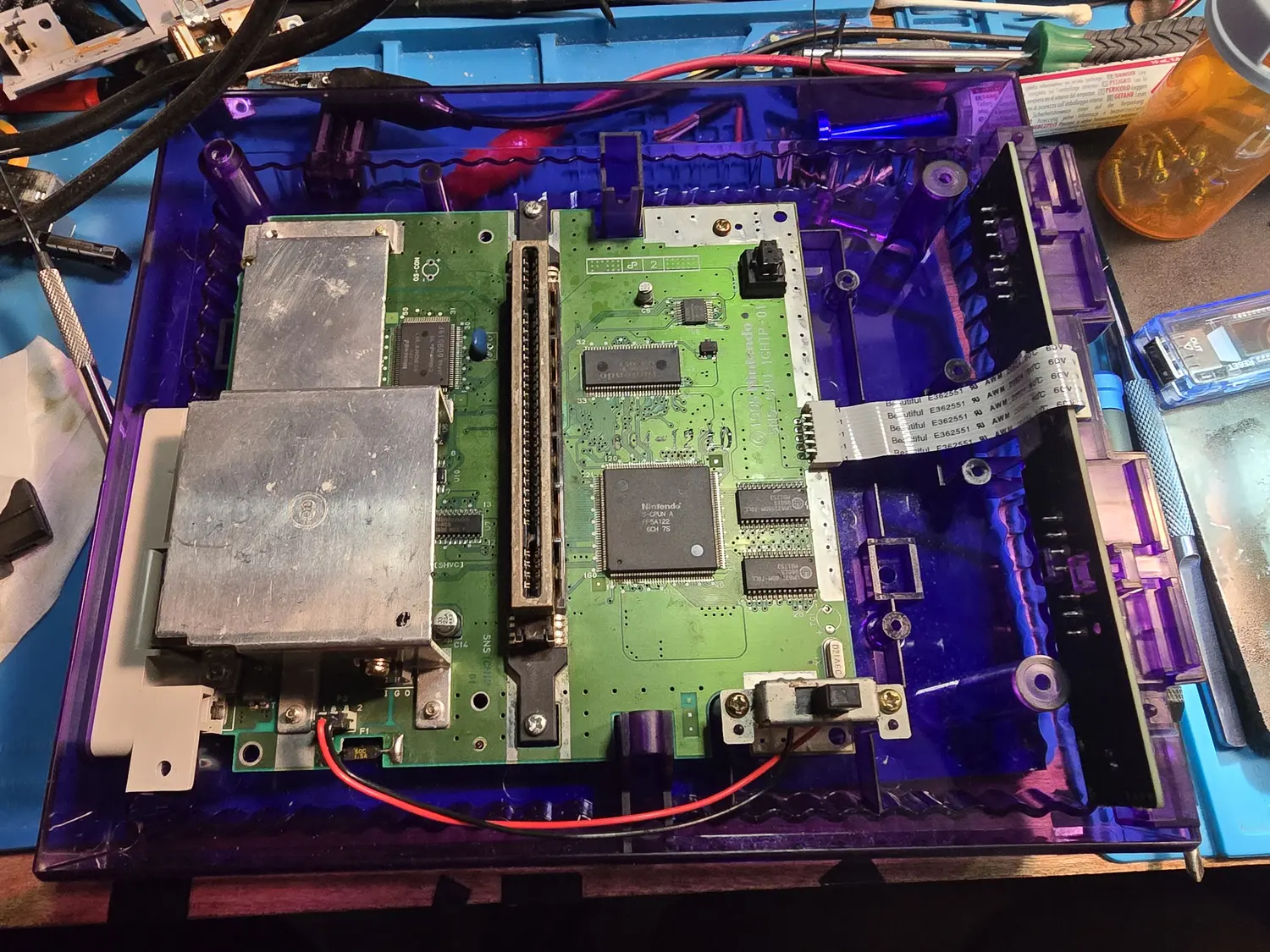
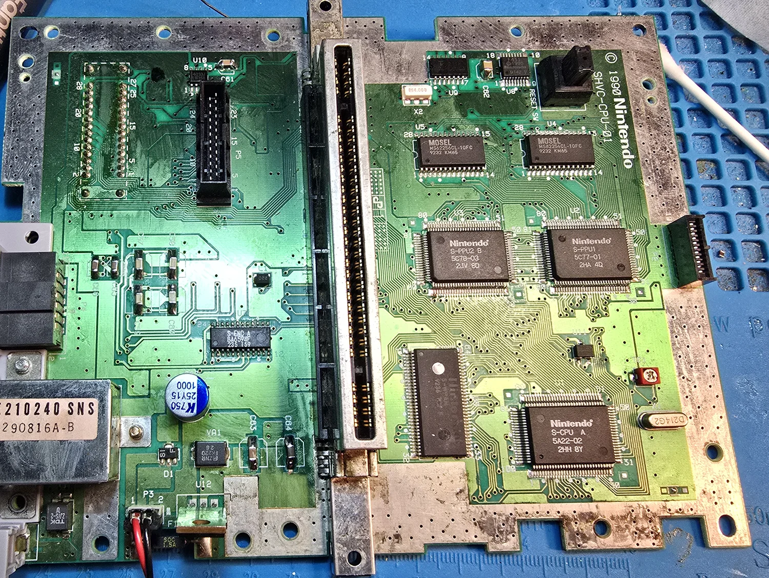
Why it matters for the picture: every S-CPUN board (all 1CHIP revisions and the Jr) outputs markedly sharper video than any multi-chip board. Within the multi-chip group SHVC-CPU-01 is the best by a hair and APU-01 is the worst. Within the 1CHIP family, do not use the sub-revision as a proxy for quality; the one review that tested many units found awful-looking -02s and phenomenal -03s, with the spread tracking component condition rather than revision.
A chart will lie to you about the U10 op-amp
One identification detail is worth a specific warning because the sources disagree. Starting somewhere in the multi-chip run, Nintendo replaced the discrete quad op-amp at reference designator U10 with its own integrated mixer, marked S-MIX. ConsoleMods says that swap began with SNS-CPU-APU-01; Console5’s per-board lists and the board photographs I have seen put S-MIX at U10 a revision or two earlier, on SNS-CPU-RGB-01. There is no chart that resolves it. Read the actual marking on the 14-pin chip at U10 on the board in front of you rather than infer it from the revision string. That is a good habit for this platform generally: the factory substituted parts, depopulated circuits, and omitted caps in ways that make any “this revision always has X” claim risky.
1CHIP or multi-chip: which one to buy
The revision above decides your picture, so it decides what to shop for. The answer splits on one question: are you going to mod it?
Stock, the 1CHIP wins and it is not close. It outputs sharp RGB from the factory, and a multi-chip board’s blur is applied ahead of the output stage, so no cable and no neutral RGB bypass recovers it. A listing claiming an RGB bypass “fixes” 2-chip blur is wrong.
Modded, a multi-chip board is the better buy. An active deblur (the open Torapu/Buttersoft filter mod, SNEdge, or Voultar’s Edge-Enhancer, all in Mods worth knowing) takes a multi-chip board to sharp. The asymmetry is what settles it: a mod fixes multi-chip blur, and no mod fixes what is wrong with a 1CHIP.
What is wrong with a 1CHIP is smaller than the word “compatibility” suggests. Games run. The S-CPUN’s DAC handles rapid writes to the brightness register poorly, which shows up as darkened scanlines at the top of the screen and wrong fade effects in a known set of titles: several Capcom games, the missing plane shadow in Air Strike Patrol, warped text boxes in Rudra. Every 1CHIP also runs its RGB hot and shows mild edge ringing. All of it is inherent to the silicon rather than a defect in any particular console, and the full detail is here. The cheap tuning is three 750 ohm resistors for brightness and a larger cap at C11 for the ringing, and C11 is a trade-off rather than an upgrade: slowing the DAC’s settling makes the fade glitch worse.
So, three situations:
- You already own a 1CHIP. You have a special machine. Fit the brightness resistors, decide on C11 by taste, and enjoy it.
- You already own a multi-chip board. Mod it. A deblur gets you the best of both, which is 1CHIP-grade sharpness with none of the S-CPUN glitches.
- You are deciding from scratch. Go multi-chip and mod it. Much cheaper, and much easier to find in good condition.
Whether the 1CHIP premium is worth paying is your call. My read is that the premium is largely an artifact of the years when a multi-chip board had no good deblur option, so buying a 1CHIP was the only route to a sharp picture. That stopped being true a while ago and the prices have not fully caught up.
Two things to check before you buy either one. The SNS-CPU-1CHIP-03 ships with its composite-sync circuit depopulated, so a CSYNC RGB cable gets no stable sync on it while a sync-on-luma cable works perfectly; that is not a fault, and not a reason to skip the board, but know which cable you own (details). And the New-Style SNS-101 and Super Famicom Jr carry the same S-CPUN silicon as a 1CHIP, composite-only from the factory, so a Jr plus an RGB restore lands in the same place as a 1CHIP for less money, with the same glitch list attached.
If you want the modded multi-chip route without doing the work, the Buttersoft filter boards I build are in the shop, as are finished consoles.
Common problems and fixes
Won’t load, freezes mid-game, or works only after reinsertion
This is the single most common fault, and it is almost always the cartridge interface rather than a chip. Start by cleaning the cartridge edge contacts with high-purity (99 percent) isopropyl alcohol and a lint-free swab, then retest two or three known-good carts. If several clean, known-good carts all misbehave the same way, the fault is the console-side 62-pin connector.
Here is where I part ways with the manufacturer. Nintendo’s own service literature is explicit that the 62-pin connector should not be cleaned, it should be replaced. I understand why they wrote that, but I do not follow it and I would not tell you to either. In my experience I have never met an SNES connector I could not clean back into reliable working order, and these connectors are not easy to source, with more than one physical type across the revisions to match on top of that. So I treat cleaning as the fix, not a stopgap: clean the console-side leaves the way you clean a cart edge, inspect them under a loupe for bent or spread contacts and gently re-tension any that need it, and reflow the connector’s solder joints on the underside, which is a common cold-joint spot. Replacement is my last resort, for a connector that is physically broken or too far gone to re-tension, not my first move. If you do replace one, note there is more than one physical 62-pin connector across SNES revisions; match the part to your board.
Dead: no light, no picture, no sound
Rule out the adapter before you open the case, and get the power spec right, because this is a console people kill with the wrong brick.
- NTSC (US SNS-001 and Japanese SHVC-001) takes 10 V DC, at least 850 mA, center-negative, unregulated. Meter an unknown brick before plugging it in: a center-positive supply is the wrong polarity here. (You will see 9 V quoted in some places; the OEM figure is 10 V DC and a 9 to 10 V DC center-negative supply is safe.) The North American jack has an inner pin specifically so a 9 V AC NES adapter cannot be inserted.
- PAL (SNSP) is different: it takes AC from the same brick as the PAL NES and rectifies it on the board, so the PAL jack tolerates either polarity. Do not feed a PAL unit a DC supply and expect it to behave like an NTSC one (more on that under the SCART hazard below).
With the adapter confirmed, the community’s reported order of no-power causes puts the DC power jack first: its plastic center post cracks with age and the joint fatigues, giving intermittent or dead power. It is a mechanical fault, and a common one. Reflow it first, and replace it if the post is loose or broken. For a replacement you have two good options: harvest a jack off a dead donor board, or buy a modern clone part for about 15 to 20 dollars. The clone is visually distinct from the original but a close match, and perfectly cromulent for getting the job done. Fair warning on the removal, though: getting the old jack off cleanly is genuinely hard without good equipment. It is a big, heat-sunk, through-hole part anchored into a ground plane, so plan on a powerful iron, a solid hot-air station, or both, and do not try it with a cheap pencil iron. This is also a job that is much easier to watch than to read, so find a good video of a SNES power-jack swap before you commit to your first one. The next suspect is the fuse, F1: 1.5 A, 125 V, fast-blow. It is a Pico axial part on the original consoles and a tiny SMD part marked F1 on the New-Style / Jr. Two things matter about it. Never fit a slow-blow substitute, because the fuse exists precisely to catch a wrong or overvoltage supply and a short to ground. And a blown fuse rarely fails on its own, so find the cause (wrong PSU, a shorted surge absorber, a downstream short) before you fit a new one and watch it pop again.
Nintendo’s own no-power priority list runs F1, then the series diode D1, then the T1 line filter, then the 7805 regulator (U12), then the VA1 surge absorber, then Q18, then the power switch (P3). The surge absorber (a small MOV) is the part nobody thinks of: a shorted VA1 pops the fuse instantly and repeatedly and looks like “the fuse keeps blowing.” Lift a leg to check it before you go hunting a downstream short.
Powers on but the screen is black or a solid color
This is the classic “it turns on but does nothing.” Work it in order:
- Confirm the reset button is not physically stuck down, which by itself blanks the screen.
- Boot a flashcart (an FXPak Pro or Everdrive). If the flashcart runs but a region-correct retail cart does not, the problem is the lockout chip, not the silicon (see region and lockout below).
- If nothing runs, split CPU from PPU. The cleanest field test is a Super Game Boy with a known-good Game Boy game: no picture at all points at a dead CPU, while a working SGB border with a game that will not load points at the PPUs. A burn-in test ROM on a flashcart is better still, because it prints an explicit “CPU FAIL” line and exercises the RAM and PPUs directly.
On the underlying cause, the repair community is fairly unified, and I want to frame this as their reported experience rather than a guarantee: once the connector and solder joints are excluded, the black-screen SNES is reported to be “nearly always” a dead CPU, with the early S-CPU / CPU-A revisions the fragile ones and VRAM a distant second. I flag that as a strong community pattern to test against, not a diagnosis to skip the testing for.
There is one case people miss, and it is worth checking early on the right board. A dead audio subsystem can present as a black screen, not merely as silence, because the CPU waits on the sound system’s boot handshake, and Nintendo’s own fault table ranks a defective sound module second for a solid-color screen, above the CPU. On most SNES boards the sound chips are soldered down, but on the original Super Famicom board (SHVC-CPU-01) the whole sound section is a plug-on module, the SHVC-SOUND daughtercard, carrying the S-SMP, S-DSP, sound RAM, DAC, and amp. On one of those, check that module first: confirm it is present, fully seated, and making clean contact. A bad connection or a bad module will either keep the console from working at all or crash it the instant a game initializes sound. In my recollection a burn-in cart may run without the module until you enter its sound test, though I would not swear to that. This is the one board where reseating and cleaning a sound module is a real, cheap first move.
The rework itself (hot-air swapping a 100-pin QFP) is routine; sourcing a good donor chip is the hard part. A CPU/PPU test socket soldered to a known-good donor board lets you swap-test a suspect chip without desoldering it, and since the S-CPU and both PPUs share the same package, one socket covers all three. It is the highest-leverage bench purchase for diagnosing dead multi-chip boards at volume.
A bright vertical line down the center of the screen
Mostly a multi-chip fault, worst at power-on and in dark scenes (Super Metroid is the canonical test). It is a voltage sag on the 5 V rail during DRAM refresh, from insufficient bypass capacitance, and it is a console fault, not a cable fault. Confirm it strengthens in dark content, then fix it one of two ways: replace the stock 7805 with a higher-current linear regulator (an ST L78S05CV-DG, 2 A) and bump the small cap on its output to 22 uF, or add a 470 uF / 16 V electrolytic across the regulator with the negative stripe to the center pin (step up to 1000 uF if 470 uF is not enough). On a 1CHIP or any board carrying an RGB bypass amp, the bypass fixes the line on the RGB output; the regulator fix is the one that also cures composite and S-video.
Left audio channel louder than the right
A design defect on the early boards only, not aging. Nintendo tied both voltage- reference pins of the NEC uPD6376 audio DAC to a single shared 47 uF capacitor where the datasheet calls for a separate cap on each, and the resulting per-channel mismatch makes the left channel hotter. It affects SHVC-CPU-01, both GPM revisions, both PAL SNSP multi-chip revisions, and SNS-CPU-RGB-01. Later boards switched to the single-reference uPD6379A DAC, which makes the imbalance structurally impossible, so they are simply unaffected. The fix is to isolate one reference pin and give it its own 47 uF cap to ground. On the SHVC-SOUND module the relevant trace runs under the chip, so you lift a pin rather than cut a trace. If you ever replace a dead late-board DAC, mind the suffix: the 6379 and 6379A latch opposite channels, so the wrong part gives you swapped stereo that passes a mono bench test and comes back as a return.
Corrupt or scrambled graphics while the game keeps running
Distinct from a black screen. On a multi-chip board this points at the video RAM (the discrete SRAM at U4/U5) first, which is cheap and socketable, then the PPUs. Mode 7 titles (Super Mario Kart, F-Zero) expose early-stage PPU faults that ordinary games hide. Before opening the console, rule out the cartridge: Nintendo’s cart-side fault table lists a dirty edge connector, the program ROM, and the cart’s own enhancement chips as causes of “confused video,” so test a few known-good carts first.
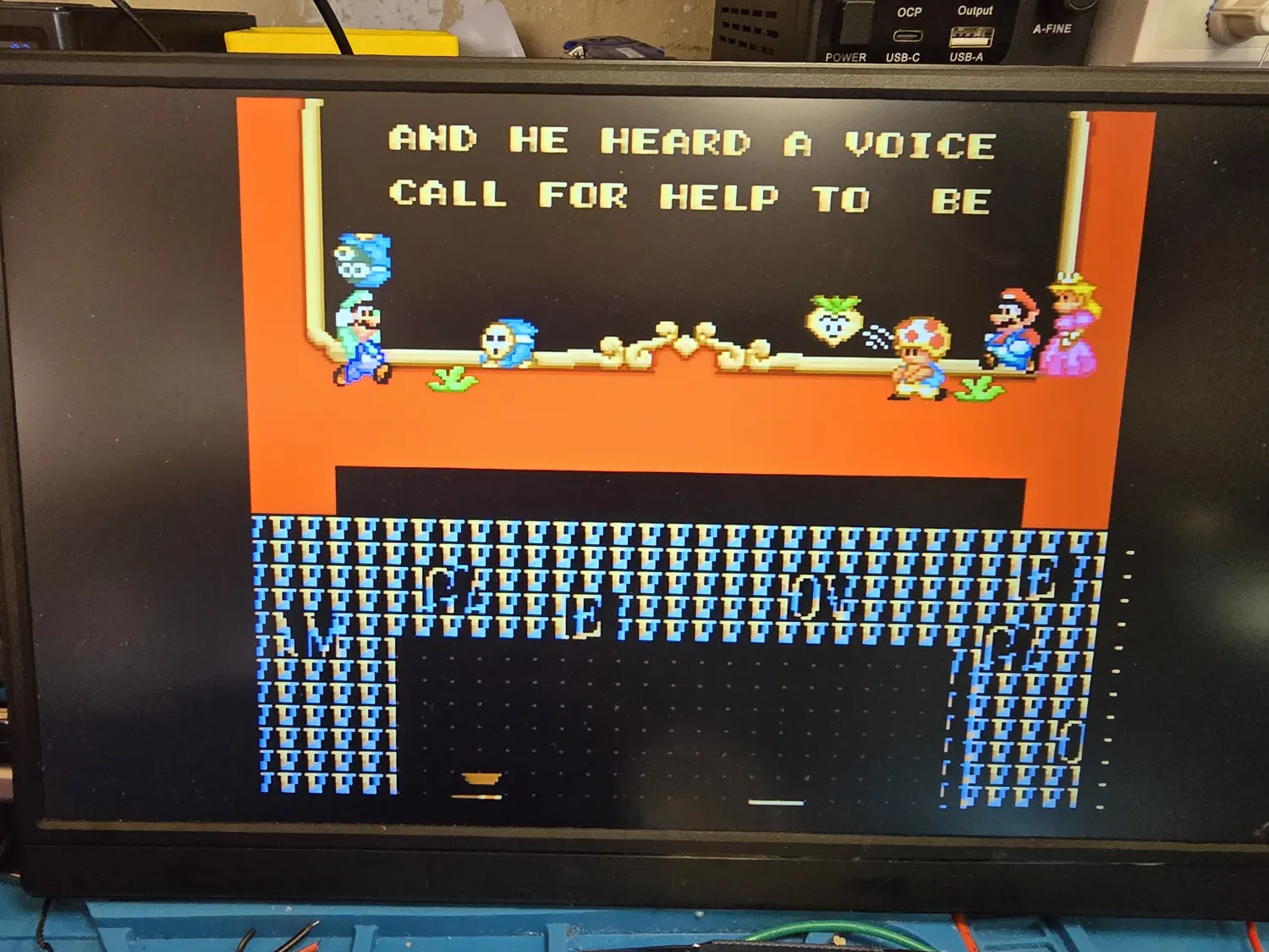
A caution from my own bench on this symptom. A burn-in or diagnostic cartridge passing every test is weaker evidence than it feels like. I have had a console clear a full diagnostic cart, run most games correctly, and still corrupt graphics reliably on specific titles, and the fix was a CPU swap. Diagnostics exercise a subset of the machine; a game exercises whatever it happens to use. If a fault reproduces perfectly on the same titles every time, trust the repeatability over the diagnostic result.
Snow or analog video artifacts
A picture that is fundamentally there but crawling with snow, speckle, or other analog artifacts is worth separating from a dead or garbled screen, because the cause is often not the console at all. The first thing I do is swap in a known-good genuine cartridge. If the artifacts clear with a good cart, the console is fine and the cartridge is the problem.
The usual culprit is a cartridge with no bus interfacing at all, which the cheapest reproduction and flash cartridges skip entirely. Running lower-voltage memory against the SNES’s 5 V cartridge bus with nothing in between puts marginal signals on the bus and dumps switching noise into the rails the video circuitry shares, and that shows up in the picture as snow or artifacts. 1CHIP consoles in particular tend to be the least forgiving of marginal cartridge-bus signals.
This cost me a lot of bench time: I once suspected three SNES consoles in a row of bad video output before working out that the cartridge was the problem. I have since opened five flash cartridges and photographed what each one puts between the edge connector and the chips, including the one that caused this. See Flash Carts, Clones and Bootlegs: What Is Actually Inside Them.
1CHIP and Jr: too bright, ringing edges, and specific game glitches
These are inherent behavior of the S-CPUN, not faults, and chasing them as defects is a waste of a bench hour. All 1CHIP consoles output RGB that runs hot (too bright and washed out) and shows mild edge ringing. The community fixes are tuning, not repair: three 750 ohm resistors into the RGB via holes brings brightness to spec (1.2 kohm on the Jr), and a larger value for the on-board cap at C11 reduces the ringing.
The ringing fix has a trade-off that listings never mention, so I will: the S-CPUN’s DAC already responds poorly to rapid writes of the brightness register, which produces darkened top-of-screen scanlines and wrong fade effects in a known set of titles (several Capcom games, Air Strike Patrol’s missing plane shadow, Rudra’s warped text boxes). The larger C11 cap slows the DAC’s settling and makes that worse. So it is a taste-and-trade-off mod, not a strict upgrade. On original carts an FXPak’s firmware brightness patch mitigates the underlying glitch (with its own caveat: it can break games that DMA to that register, like Star Fox, so it ships off and is enabled per game).
No RGB sync on a CSYNC cable (1CHIP-03), and the PAL sync hazard
The SNS-CPU-1CHIP-03 revision ships with its composite-sync output circuit depopulated, so a CSYNC (pin 3) RGB cable gets no stable sync while a sync-on-luma cable works perfectly. That split is the -03 fingerprint. The easy answer is a sync-on-luma cable with no mod at all; the proper restore repopulates the missing sync components, and the cleanest path for a modded unit is an RGB bypass board that carries its own sync circuit.
Separately, and this one can cost you equipment: a PAL SNES puts 12 V on multi-out pin 3 for SCART autoswitching, where an NTSC unit puts a TTL sync signal. Connecting an NTSC CSYNC cable to a PAL SNES can damage your gear. Take sync from luma (pin 7) or composite (pin 9) on PAL. And if a PAL unit “stopped auto-switching the TV to 4:3,” suspect that someone ran it on a DC supply: the 12 V comes from a doubler that only reaches 12 V on the correct AC input, and sits around 7.5 V on DC, too low to trigger the switch. That is not a board fault.
Cosmetic: yellowed shells and hidden corrosion
The ABS shells yellow over time from UV and the bromine flame retardant in the plastic, and it is purely cosmetic. Retrobrighting brings the color back for resale. While the shielding is off, check under the RF can for corrosion that has not yet become an electrical fault; neutralize and clean it before it eats a trace.
![A SNES mainboard corner with the RF shielding removed and the DC barrel jack desoldered out, exposing a large rectangular area of orange-brown corrosion crust spreading across the solder mask, the module's mounting pads and the vacated jack footprint, which sits against large tinned ground areas. Nearby silkscreen reads P4, P3, J2, U9, VA1 and D1[SHVCJ], with a 1.5 A fuse and several electrolytic capacitors marked 33uF 25V and 47uF 16V visible at the lower edge.](/reference/snes/corrosion-under-rf-module.webp)
I use the same corrosion process described in my restoration and testing writeup, then re-validate function separately.
Repairing a snapped-off edge connector
Reddit user Hungry4Italy posted a SHVC-BJ1M-20 board, a 1994
battery-backed save cart, with the whole gold-finger strip separated from the
board across its full width. Not cracked, not lifting at one corner. Off, in one
piece. Both photographs here are his, used with permission; the
original thread is on r/snes
and is worth reading for the replies as well.
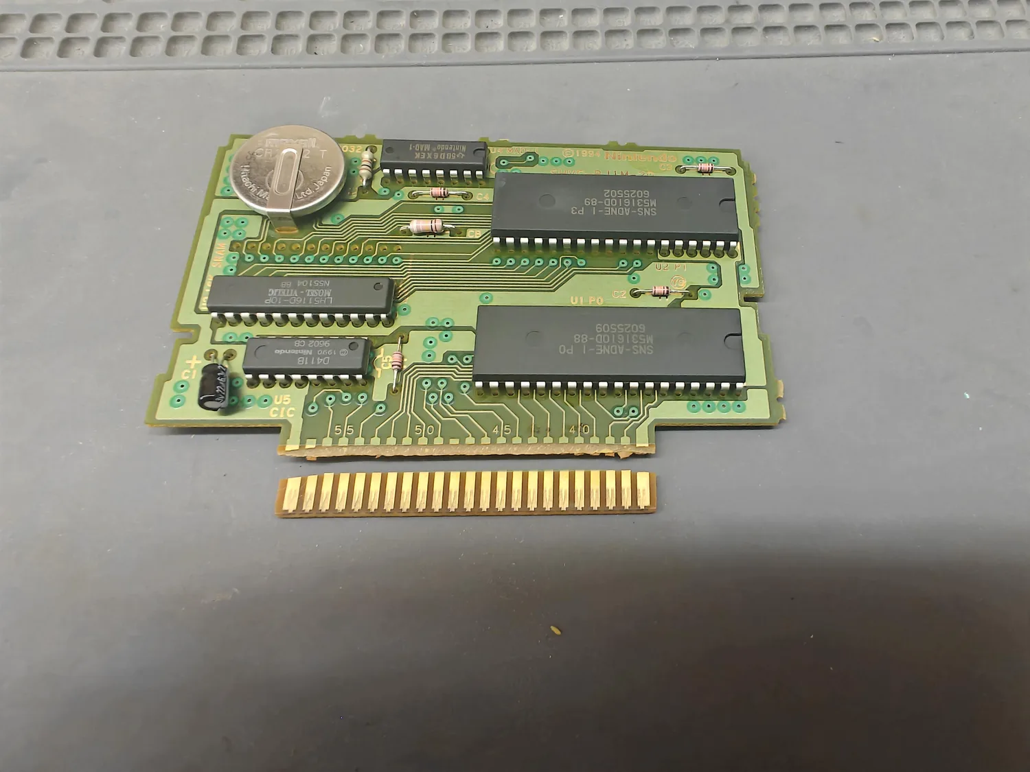
He got it working again.
Not my greatest solder job, but after using 2 part epoxy and a clamp to repair the broken piece, I scratched the PCB to expose the copper and soldered the joint. Epoxy is extremely strong and it all works now.
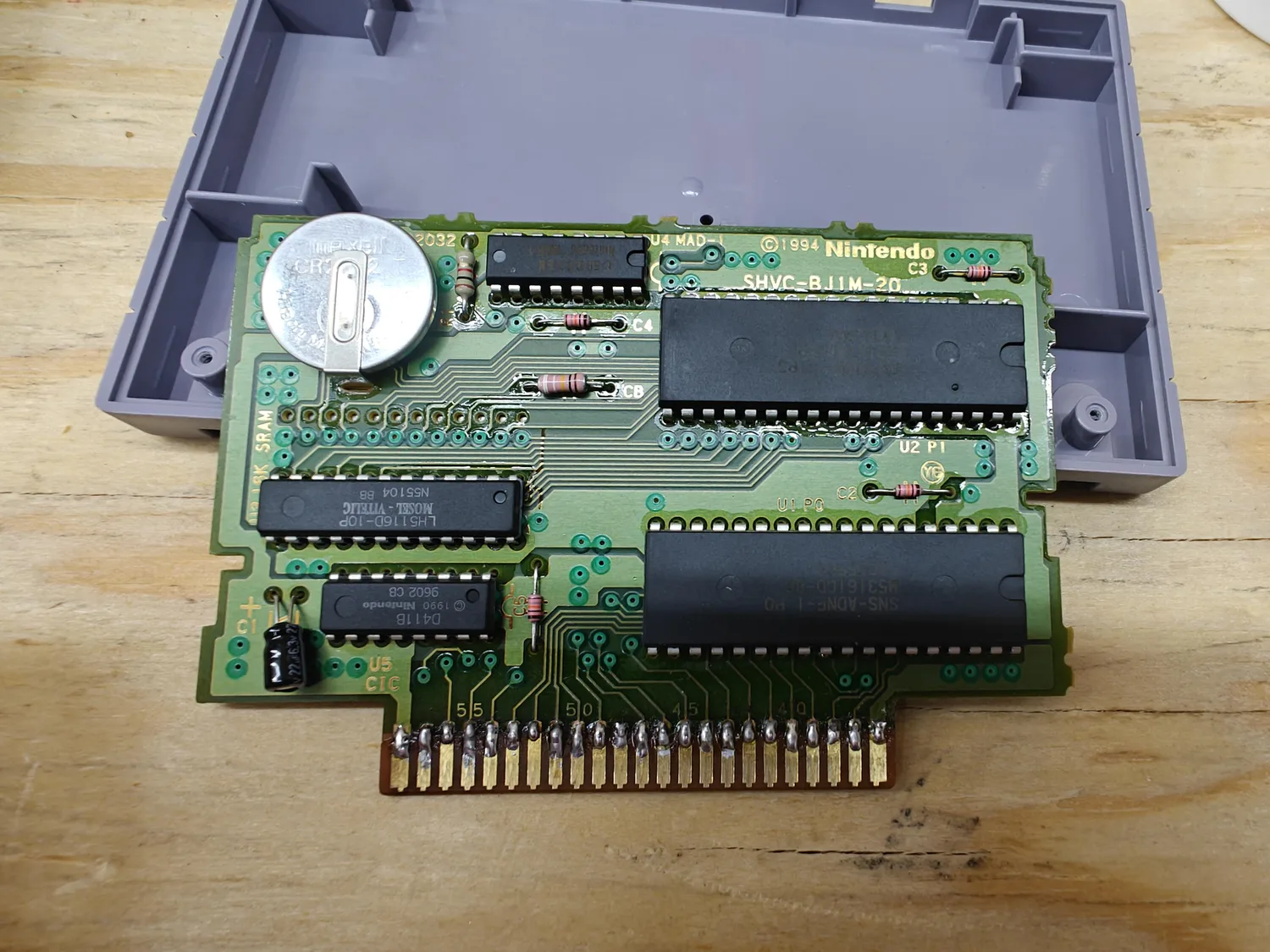
Epoxy carries the load, solder carries the signal. Solder has no useful mechanical strength across a break that a cartridge slot works on every insertion, so the joint cannot do both jobs. Scratching back to bare copper on each side of the break is what turns thirty-odd interrupted traces into conductors again.
Cartridges from the first few generations are simple. The parts are large, most of them are through-hole, and the traces are wide enough to see and wide enough to put an iron on. Nothing on this board sits at a pitch that needs a microscope. People will tell you a repair like this is not economical, and they are usually right. With enough effort it can still be done.
One thing to get right if you copy it: keep the joints flat. A proud blob on a cart edge spreads or scores the console’s 62-pin leaves, and you find that out later, on other carts. He went back and reduced the ones he had built too high after another commenter raised it. Keep them at the top of the finger area, away from the leading edge, and test the repaired cart in the console you care least about.
It broke because the cart was knocked while it was inserted, and the crack grew from there over months before it finally let go.
I have not done this repair myself, so I cannot tell you how it holds up over a few hundred insertions or whether the epoxy minds a warm console. If your cart is a common one, a donor board and a ROM transplant is less work.
Region, 50/60 Hz, and SFC to SNES conversion
Region is two separate barriers that need different fixes, and confusing them wastes effort.
The first is cartridge shape. Japanese, PAL and Korean carts use the rounded shell; North American and Brazilian carts use the blocky one. All regions share the exact same cartridge connector and pinout. A US console physically blocks Japanese and PAL carts with two plastic tabs at the back of the slot, which you can cut out or replace with a tab-free insert (use the insert on anything with collector value).
The second is the lockout chip (CIC). All NTSC consoles (Japan, Korea, US, Brazil) use the same F411 family; all PAL consoles use F413. The consequence people miss: a Japanese cart in a US console is only blocked by the slot tabs, not by lockout, because both are NTSC F411. So playing imports on a US machine can be purely mechanical, with no CIC mod at all. A true region change (PAL to NTSC or the reverse) is where you defeat or replace the lockout. The modern answer is a drop-in region-free CIC board (SuperCIC and similar), most of which also add a switchless 50/60 Hz toggle. Keep a CIC-on mode available: some SA-1 titles (Super Mario RPG, Kirby Super Star) detect a disabled CIC and refuse to boot, so ship a switch, never a permanent disable.
A 50/60 Hz switch changes only the video timing, not the color encoding. A PAL board forced to 60 Hz can still show black-and-white on a color-fussy set, because you have not converted PAL color to NTSC color, only the refresh rate. The fix for that is a display that syncs both, not more soldering.
That shared NTSC lockout is also what makes the Super Famicom to SNES conversion worthwhile: drop a cheap, plentiful Japanese 1CHIP board into a US shell and it plays US carts natively with no CIC or 50/60 Hz mod, because the only thing that ever blocked those carts was the slot tabs in the shell. Four things actually bite: match the shell generation to the board (the earliest four-foot SHVC-CPU-01 cases do not interchange with the later two-foot cases), deal with the cart-slot tabs, ship the correct 10 V DC center-negative brick wound for local mains, and do not attempt this with a PAL board (its on-board AC rectifier and 12 V doubler make it a poor fit for a US shell and supply). If you sell a converted unit, disclose it: it is a genuine Nintendo board in a genuine Nintendo shell, but the case serial will not match the board revision inside, which is exactly the check a knowledgeable 1CHIP buyer runs.
Mods worth knowing
RGB is already good on a stock NTSC SNES, which is the platform’s happy surprise, so the mods here are about matching the output to a modern display and about recovering the sharpness the multi-chip boards throw away. I do not reproduce anyone’s install guide or schematic; this is an orientation with pointers to the real instructions.
- The governing fact: a multi-chip board’s blur cannot be undone by a neutral buffer or RGB bypass. It needs an active deblur or sharpener. A 1CHIP or Jr is already sharp and needs only cheap tuning. The most common overclaim in SNES listings is that an RGB bypass “fixes” 2-chip blur; it does not.
- Multi-chip sharpening. The low-cost open path is the Torapu / Buttersoft filter mod (a per-channel op-amp and RC network built from cheap parts), documented in amaiorano’s per-revision build guides. The open THS7376-based SNEdge is an active sharpener, fab-it-yourself under an open-hardware license (NTSC tested, PAL still experimental). The turnkey commercial option is Voultar’s Edge-Enhancer, the one board that also cleans composite and S-video.
- RGB bypass and cleanup for all revisions. borti4938’s open SNES RGB Bypass (THS7374) comes in base, CSYNC and CSYNC-plus-S-video variants; the licensing across borti’s boards is mixed, so check the repo before you build or sell. RetroSix’s CleanRGB fixes the DC offset at the console so a purely passive cable works.
- 1CHIP tuning: the 750 ohm brightness resistors and the C11 ghosting cap described above are the near-mandatory cheap wins on any 1CHIP RGB unit, with the C11 trade-off in mind.
- Dejitter is a scaler-specific fix, not a picture upgrade. It matters only if the buyer runs a simple line-doubler that mishandles the SNES’s shortened scanline, and it can cause composite or S-video flicker on some boards, so leave it off by default. marqs85’s and borti4938’s dejitter designs are the references.
- Digital audio (S/PDIF) taps the sound DSP for a bit-exact optical or coax output. Two limitations to disclose: Super Game Boy audio and MSU-1 soundtrack audio are generated outside the SNES sound chips, so neither appears on the digital output.
One mod to never do or ship: the old 2-chip “YPbPr” component mod. ConsoleMods keeps its guide only for historical reasons and warns it can damage the video encoder. Use an HD Retrovision transcoding cable if you want component out.
If you would rather buy an SNES with the RGB and region work already done, everything I restore is in the shop.
Recap and parts
The SNES is not a routine-recap console, and the mass-leak advisories that exist for a Game Gear have no SNES equivalent. Its electrolytics are small audio-coupling and decoupling caps, not switcher caps under ripple stress, so the community consensus (which I share here as the sensible default) is to recap on symptoms: muffled or weak audio, audible bias noise, bulging or leaking cans, or as belt-and-suspenders on a resale unit you already have open. The one genuinely age-sensitive area is the SHVC-SOUND module on the earliest Super Famicom, whose caps sit inside a shielded module you have to pry open.
Practical notes:
- Board-specific cap kits exist (Console5 sells them per revision, leaded or SMD), and the cap values and designators differ by board, so identify the revision first. Read the value off the can and the silkscreen before you desolder; the published cap maps are a single-origin reference, good but worth cross-checking against the physical part.
- There is a documented conflict over whether the big 1000 uF reservoir cap (C67 / C58 depending on board) is even populated on North American boards. One source says it is factory-omitted on US units; the NTSC schematic shows it present. Do not assume a missing bulk cap on a US board is a prior repair, and do not assume it is there either. Look at the pads. If they are empty, populating that cap is essentially the same intervention as the vertical-line “add a bulk cap” fix.
- Fuse F1 is 1.5 A, 125 V, fast-blow: a Littelfuse 251-series Pico axial on the original consoles, a Littelfuse 451-series Nano SMD on the New-Style / Jr. Never a slow-blow.
- The 7805 regulator (U12) runs hot by design, dropping 10 V to 5 V linearly, and the heat alone is not a fault. If you replace it, keep it linear. Switching drop-in modules run cool but can inject rolling lines into the picture, and this is not a 5 V-only console: the raw input rail also feeds the video and audio circuitry through a transistor follower, so do not follow the common “run the regulator from 7.5 V to reduce heat” advice here, and do not skip the regulator and feed 5 V straight in.
- A few Japanese discrete parts and the Nintendo-custom mechanical parts (the DC jack, the 62-pin connector) have no distributor part number. Order them from a retro-parts vendor or harvest a donor. On a fleet, the worst board is your parts stock.
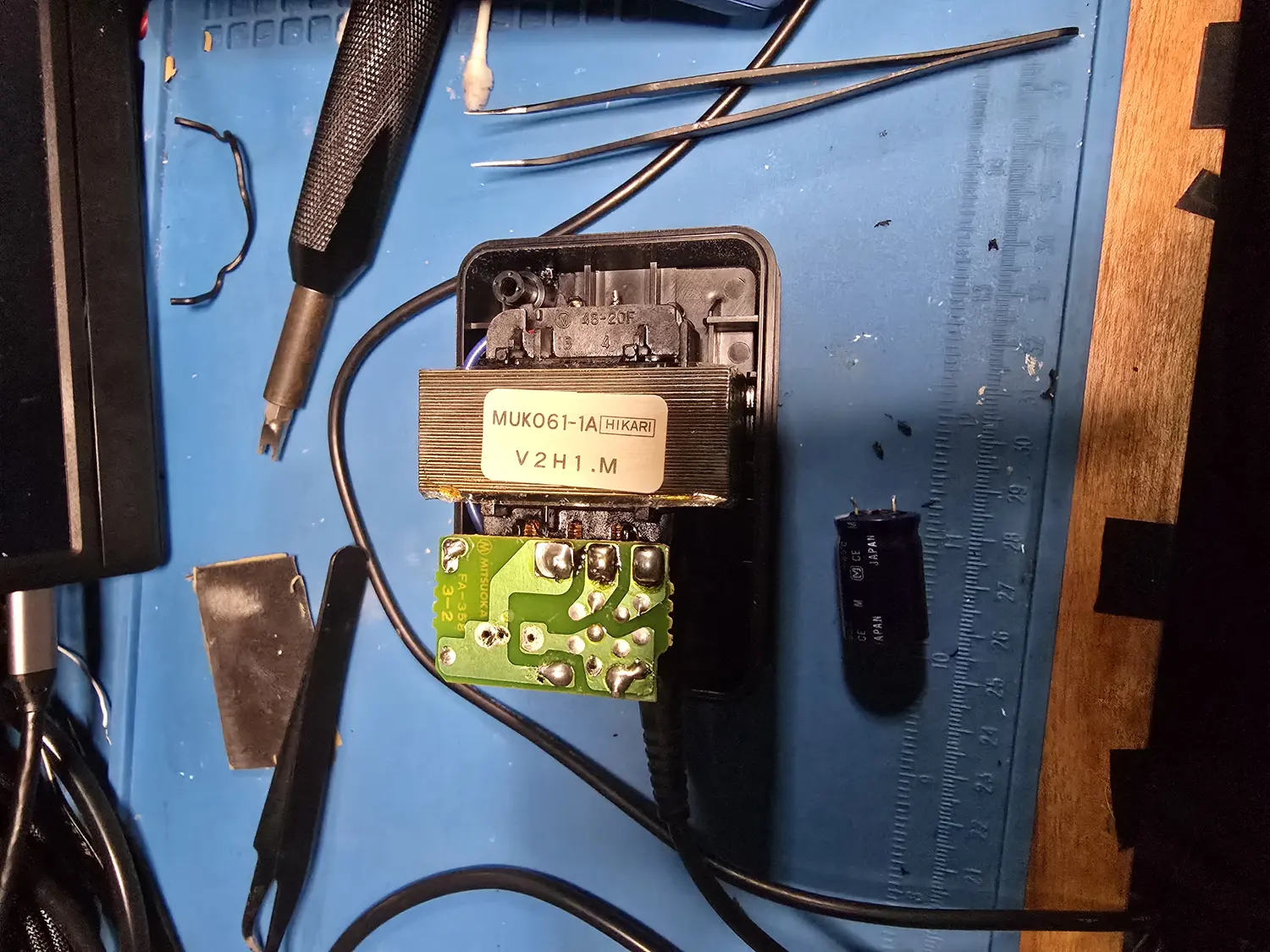
Test every unit with an enhancement-chip cartridge (Star Fox for Super FX, Super Mario RPG for SA-1) before you list it. Those carts are the only ones that use the outer pin groups of the slot and the only ones that load the 5 V rail hard, so a board that is marginal on power or has dirty outer contacts will pass a Super Mario World smoke test and fail for the buyer.
The data behind all of this
Everything above is the reasoning; what follows is the raw reference material I work from at the bench, structured so you can actually use it. It is folded by default because there is a lot of it. Expand any row or card for the detail, and note the confidence tag on every line, because a fair amount of this platform’s published data comes from a single source.
Capacitor lists
Per-revision electrolytic maps. The board revision decides the designators as well as the values here (the whole board renumbers at SNS-CPU-RGB-01, and the Jr has a list of its own), so identify the board before you order a kit.
SHVC-CPU-01 SHVC-CPU-01: multi-chip, plug-on SHVC-SOUND module (NTSC, 1990–1992)
Board p/n: SHVC-CPU-01 (JP / US / KR)
Main board — electrolytics
| Desig | Value | V | OEM p/n | Substitute | Note |
|---|---|---|---|---|---|
| C57 | 100 µF | 6 V | 100 µF, ≥10 V, 105 °C aluminium (6 V stock is a tight rating; going up is free) | SHVC-only value: later boards use 220 µF/6.3 V here single sourcec5,c5-capmap | |
| C58 | 100 µF | 6 V | 100 µF, ≥10 V, 105 °C aluminium | single sourcec5,c5-capmap | |
| C59 | 100 µF | 6 V | 100 µF, ≥10 V, 105 °C aluminium | single sourcec5,c5-capmap | |
| C60 | 100 µF | 6 V | 100 µF, ≥10 V, 105 °C aluminium | single sourcec5,c5-capmap | |
| C61 | 10 µF | 16 V | 10 µF, ≥16 V, 105 °C aluminium | single sourcec5,c5-capmap | |
| C62 | 2.2 µF | 50 V | 2.2 µF, ≥50 V, 105 °C aluminium | CIC power-on delay: this is the cap on CIC pin 3 single sourcec5,c5-capmap,sch-pal | |
notes on C62The PAL schematic ties C62 (2.2 µF/50 V) to CIC pin 3 as the
power-on delay. Same designator and value appears on every SNES
revision I have a list for, so the role almost certainly carries
across, but I have only seen it drawn on the PAL sheet. | |||||
| C63 | 33 µF | 25 V | 33 µF, ≥25 V, 105 °C aluminium | regulator input side single sourcec5,c5-capmap,sch-ntsc | |
| C64 | 33 µF | 25 V | 33 µF, ≥25 V, 105 °C aluminium | single sourcec5,c5-capmap | |
| C65 | 10 µF | 16 V | 10 µF, ≥16 V, 105 °C aluminium | single sourcec5,c5-capmap | |
| C66 | 10 µF | 16 V | 10 µF, ≥16 V, 105 °C aluminium | single sourcec5,c5-capmap | |
| C67 | 1000 µF | 25 V | 1000 µF, ≥25 V, 105 °C low-ESR | the main reservoir: Console5 says it is unpopulated on North American boards from late SHVC-CPU-01 onward single sourcec5,cm-diff,sch-ntsc | |
notes on C67Two good sources disagree about this position and I have not resolved it. Console5 and ConsoleMods both say the 1000 µF reservoir is factory-omitted on North American boards; the NTSC schematic, drawn for the NTSC boards, shows it populated. Practical handling: look at the pads. If they are empty on a US board, do not assume a previous repair pulled the cap: and populating it with a 1000 µF/25 V is essentially free and is the same intervention as the vertical-line bulk-cap fix. | |||||
SHVC-SOUND plug-on module — electrolytics
| Desig | Value | V | OEM p/n | Substitute | Note |
|---|---|---|---|---|---|
| C50 | 47 µF | 10 V | 47 µF, ≥10 V, 105 °C aluminium | audio section: see notes before you cut anything here single sourcec5,c5-capmap,cm-audio | |
notes on C50C50 and C51 are the only two electrolytics on the sound module, and they are why a SHVC-CPU-01 recap is a bigger job than the cap count suggests: the module unscrews from the main board with two JIS screws and then its shielding has to be pried off before you can reach either one. Which of the two is the DAC’s shared voltage-reference cap is not settled. Both are 47 µF/10 V, ConsoleMods says both µPD6376 Vref pins share a single 47 µF against the datasheet, so one of these is that cap and the other serves something else. Confirm against the actual DAC pins before treating either as the audio-balance-fix position. If you are doing the balance fix on this board, note the SHVC-only procedure: lift DAC pin 9 rather than cutting the pin 9/10 trace, because that trace runs underneath the DAC. Space inside the shielding is tight, so fit the smallest 47 µF you can get. | |||||
| C51 | 47 µF | 10 V | 47 µF, ≥10 V, 105 °C aluminium | audio section: see the C50 notes single sourcec5,c5-capmap | |
SNS-CPU-GPM-01 SNS-CPU-GPM-01: multi-chip, audio moves onto the main board (NTSC, 1992)
Board p/n: SNS-CPU-GPM-01
Main board — electrolytics
| Desig | Value | V | OEM p/n | Substitute | Note |
|---|---|---|---|---|---|
| C57 | 220 µF | 6.3 V | 220 µF, ≥6.3 V, 105 °C aluminium | audio output coupling single sourcec5,c5-capmap | |
| C59 | 220 µF | 6.3 V | 220 µF, ≥6.3 V, 105 °C aluminium | single sourcec5,c5-capmap | |
| C61 | 10 µF | 16 V | 10 µF, ≥16 V, 105 °C aluminium | single sourcec5,c5-capmap | |
| C62 | 2.2 µF | 50 V | 2.2 µF, ≥50 V, 105 °C aluminium | CIC power-on delay single sourcec5,c5-capmap | |
| C63 | 33 µF | 25 V | 33 µF, ≥25 V, 105 °C aluminium | regulator input side single sourcec5,c5-capmap | |
| C64 | 33 µF | 25 V | 33 µF, ≥25 V, 105 °C aluminium | single sourcec5,c5-capmap | |
| C65 | 10 µF | 16 V | 10 µF, ≥16 V, 105 °C aluminium | single sourcec5,c5-capmap | |
| C66 | 10 µF | 16 V | 10 µF, ≥16 V, 105 °C aluminium | single sourcec5,c5-capmap | |
| C67 | 1000 µF | 25 V | 1000 µF, ≥25 V, 105 °C low-ESR | Console5: not present on North American units. Check the pads before you conclude anything single sourcec5,cm-diff,sch-ntsc | |
notes on C67Same unresolved conflict as on SHVC-CPU-01: Console5 and
ConsoleMods call this factory-omitted on NA boards, the NTSC
schematic shows it fitted. Look at the pads. | |||||
| C73 | 47 µF | 16 V | 47 µF, ≥16 V, 105 °C aluminium | the DAC voltage-reference cap: the audio-balance defect lives here single sourcec5,c5-capmap,sch-pal,cm-audio | |
notes on C73On the PAL schematic, C73 (47 µF) is the single cap that both Vref
pins of the µPD6376 are tied to. The shared-reference wiring that
causes the channel imbalance. This board carries the same
designator, the same value and the same DAC, so the balance fix
lands here: isolate DAC pin 10 by cutting the pin 9–10 trace, then
hang a fresh 47 µF (≥10 V) on the isolated pin, positive to the
pin, negative to ground. | |||||
SNS-CPU-GPM-02 SNS-CPU-GPM-02: multi-chip, last removable cart port (NTSC, 1993–1994)
Board p/n: SNS-CPU-GPM-02 · SNSM-CPU-GPM-02 (Brazil, PAL-M)
Main board — electrolytics
| Desig | Value | V | OEM p/n | Substitute | Note |
|---|---|---|---|---|---|
| C57 | 220 µF | 6.3 V | 220 µF, ≥6.3 V, 105 °C aluminium | Console5 gives GPM-01 and GPM-02 one shared cap list single sourcec5,c5-capmap | |
| C59 | 220 µF | 6.3 V | 220 µF, ≥6.3 V, 105 °C aluminium | single sourcec5,c5-capmap | |
| C61 | 10 µF | 16 V | 10 µF, ≥16 V, 105 °C aluminium | single sourcec5,c5-capmap | |
| C62 | 2.2 µF | 50 V | 2.2 µF, ≥50 V, 105 °C aluminium | CIC power-on delay single sourcec5,c5-capmap | |
| C63 | 33 µF | 25 V | 33 µF, ≥25 V, 105 °C aluminium | regulator input side single sourcec5,c5-capmap | |
| C64 | 33 µF | 25 V | 33 µF, ≥25 V, 105 °C aluminium | single sourcec5,c5-capmap | |
| C65 | 10 µF | 16 V | 10 µF, ≥16 V, 105 °C aluminium | single sourcec5,c5-capmap | |
| C66 | 10 µF | 16 V | 10 µF, ≥16 V, 105 °C aluminium | single sourcec5,c5-capmap | |
| C67 | 1000 µF | 25 V | 1000 µF, ≥25 V, 105 °C low-ESR | Console5: not present on North American units. Check the pads single sourcec5,cm-diff,sch-ntsc | |
| C73 | 47 µF | 16 V | 47 µF, ≥16 V, 105 °C aluminium | DAC voltage-reference cap: audio-balance defect position single sourcec5,c5-capmap,sch-pal,cm-audio | |
notes on C73Same position as on GPM-01: the single shared cap across the
µPD6376’s two Vref pins. Isolate pin 10 and give it its own 47 µF
to fix the imbalance. | |||||
SNS-CPU-RGB-01 SNS-CPU-RGB-01: multi-chip, new encoder kills the discrete RGB amp (NTSC, 1994)
Board p/n: SNS-CPU-RGB-01
Main board — electrolytics
| Desig | Value | V | OEM p/n | Substitute | Note |
|---|---|---|---|---|---|
| C9 | 2.2 µF | 50 V | 2.2 µF, ≥50 V, 105 °C aluminium | the whole board renumbers here: Console5 gives RGB-01, RGB-02 and APU-01 one shared list single sourcec5,c5-capmap | |
| C12 | 10 µF | 16 V | 10 µF, ≥16 V, 105 °C aluminium | single sourcec5,c5-capmap | |
| C13 | 10 µF | 16 V | 10 µF, ≥16 V, 105 °C aluminium | single sourcec5,c5-capmap | |
| C14 | 33 µF | 25 V | 33 µF, ≥25 V, 105 °C aluminium | single sourcec5,c5-capmap | |
| C15 | 47 µF | 16 V | 47 µF, ≥16 V, 105 °C aluminium | this board still uses the two-Vref µPD6376, so it still has the audio-balance defect single sourcec5,c5-capmap,cm-audio | |
notes on C15RGB-01 is the last board with the µPD6376, so it is the last board
with the balance defect. The fix is at the DAC (isolate pin 10, own
47 µF), not necessarily at this designator: I have not seen the
Vref cap identified by designator on this board. | |||||
| C16 | 33 µF | 25 V | 33 µF, ≥25 V, 105 °C aluminium | single sourcec5,c5-capmap | |
| C17 | 33 µF | 25 V | 33 µF, ≥25 V, 105 °C aluminium | single sourcec5,c5-capmap | |
| C18 | 220 µF | 6.3 V | 220 µF, ≥6.3 V, 105 °C aluminium | audio output coupling single sourcec5,c5-capmap | |
| C19 | 220 µF | 6.3 V | 220 µF, ≥6.3 V, 105 °C aluminium | single sourcec5,c5-capmap | |
| C58 | 1000 µF | 25 V | 1000 µF, ≥25 V, 105 °C low-ESR | the reservoir moves from C67 to C58 on this generation. Console5: not present on North American units. single sourcec5,cm-diff | |
SNS-CPU-RGB-02 SNS-CPU-RGB-02: multi-chip, S-RGB encoder and the DAC that fixes the audio balance (NTSC, 1995)
Board p/n: SNS-CPU-RGB-02
Main board — electrolytics
| Desig | Value | V | OEM p/n | Substitute | Note |
|---|---|---|---|---|---|
| C9 | 2.2 µF | 50 V | 2.2 µF, ≥50 V, 105 °C aluminium | single sourcec5,c5-capmap | |
| C12 | 10 µF | 16 V | 10 µF, ≥16 V, 105 °C aluminium | single sourcec5,c5-capmap | |
| C13 | 10 µF | 16 V | 10 µF, ≥16 V, 105 °C aluminium | single sourcec5,c5-capmap | |
| C14 | 33 µF | 25 V | 33 µF, ≥25 V, 105 °C aluminium | single sourcec5,c5-capmap | |
| C15 | 47 µF | 16 V | 47 µF, ≥16 V, 105 °C aluminium | this board runs the single-Vref µPD6379A: no balance defect to fix single sourcec5,c5-capmap,cm-audio | |
| C16 | 33 µF | 25 V | 33 µF, ≥25 V, 105 °C aluminium | single sourcec5,c5-capmap | |
| C17 | 33 µF | 25 V | 33 µF, ≥25 V, 105 °C aluminium | single sourcec5,c5-capmap | |
| C18 | 220 µF | 6.3 V | 220 µF, ≥6.3 V, 105 °C aluminium | single sourcec5,c5-capmap | |
| C19 | 220 µF | 6.3 V | 220 µF, ≥6.3 V, 105 °C aluminium | single sourcec5,c5-capmap | |
| C58 | 1000 µF | 25 V | 1000 µF, ≥25 V, 105 °C low-ESR | Console5: not present on North American units single sourcec5,cm-diff |
SNS-CPU-APU-01 SNS-CPU-APU-01: final multi-chip board, audio fused into one S-APU (NTSC, 1995–1996)
Board p/n: SNS-CPU-APU-01
Main board — electrolytics
| Desig | Value | V | OEM p/n | Substitute | Note |
|---|---|---|---|---|---|
| C9 | 2.2 µF | 50 V | 2.2 µF, ≥50 V, 105 °C aluminium | same list as RGB-01/-02: the board lost U15–U17, not caps single sourcec5,c5-capmap | |
| C12 | 10 µF | 16 V | 10 µF, ≥16 V, 105 °C aluminium | single sourcec5,c5-capmap | |
| C13 | 10 µF | 16 V | 10 µF, ≥16 V, 105 °C aluminium | single sourcec5,c5-capmap | |
| C14 | 33 µF | 25 V | 33 µF, ≥25 V, 105 °C aluminium | single sourcec5,c5-capmap | |
| C15 | 47 µF | 16 V | 47 µF, ≥16 V, 105 °C aluminium | single sourcec5,c5-capmap | |
| C16 | 33 µF | 25 V | 33 µF, ≥25 V, 105 °C aluminium | single sourcec5,c5-capmap | |
| C17 | 33 µF | 25 V | 33 µF, ≥25 V, 105 °C aluminium | single sourcec5,c5-capmap | |
| C18 | 220 µF | 6.3 V | 220 µF, ≥6.3 V, 105 °C aluminium | single sourcec5,c5-capmap | |
| C19 | 220 µF | 6.3 V | 220 µF, ≥6.3 V, 105 °C aluminium | single sourcec5,c5-capmap | |
| C58 | 1000 µF | 25 V | 1000 µF, ≥25 V, 105 °C low-ESR | Console5: not present on North American units single sourcec5,cm-diff |
SNS-CPU-1CHIP-01 SNS-CPU-1CHIP-01: first 1CHIP, S-CPUN (NTSC, 1995)
Board p/n: SNS-CPU-1CHIP-01 · SNSM-CPU-1CHIP-01 (Brazil, PAL-M)
Main board — electrolytics
| Desig | Value | V | OEM p/n | Substitute | Note |
|---|---|---|---|---|---|
| C9 | 2.2 µF | 50 V | 2.2 µF, ≥50 V, 105 °C aluminium | Console5 gives 1CHIP-01, -02 and -03 one shared list, identical to the RGB/APU list single sourcec5,c5-capmap | |
| C12 | 10 µF | 16 V | 10 µF, ≥16 V, 105 °C aluminium | single sourcec5,c5-capmap | |
| C13 | 10 µF | 16 V | 10 µF, ≥16 V, 105 °C aluminium | single sourcec5,c5-capmap | |
| C14 | 33 µF | 25 V | 33 µF, ≥25 V, 105 °C aluminium | single sourcec5,c5-capmap | |
| C15 | 47 µF | 16 V | 47 µF, ≥16 V, 105 °C aluminium | single sourcec5,c5-capmap | |
| C16 | 33 µF | 25 V | 33 µF, ≥25 V, 105 °C aluminium | single sourcec5,c5-capmap | |
| C17 | 33 µF | 25 V | 33 µF, ≥25 V, 105 °C aluminium | single sourcec5,c5-capmap | |
| C18 | 220 µF | 6.3 V | 220 µF, ≥6.3 V, 105 °C aluminium | single sourcec5,c5-capmap | |
| C19 | 220 µF | 6.3 V | 220 µF, ≥6.3 V, 105 °C aluminium | single sourcec5,c5-capmap | |
| C58 | 1000 µF | 25 V | 1000 µF, ≥25 V, 105 °C low-ESR | Console5: not present on North American units single sourcec5,cm-diff | |
notes on C58Do not sweep C11 into a recap of this board. On a 1CHIP, C11 is a
0.47 µF ceramic, not an electrolytic: it is the ghosting-fix cap,
and it is listed in the replacement-parts table instead. | |||||
SNS-CPU-1CHIP-02 SNS-CPU-1CHIP-02: 1CHIP, largely identical to -01 (NTSC, 1995–1997)
Board p/n: SNS-CPU-1CHIP-02 · SNSM-CPU-1CHIP-02 (Brazil, PAL-M)
Main board — electrolytics
| Desig | Value | V | OEM p/n | Substitute | Note |
|---|---|---|---|---|---|
| C9 | 2.2 µF | 50 V | 2.2 µF, ≥50 V, 105 °C aluminium | single sourcec5,c5-capmap | |
| C12 | 10 µF | 16 V | 10 µF, ≥16 V, 105 °C aluminium | single sourcec5,c5-capmap | |
| C13 | 10 µF | 16 V | 10 µF, ≥16 V, 105 °C aluminium | single sourcec5,c5-capmap | |
| C14 | 33 µF | 25 V | 33 µF, ≥25 V, 105 °C aluminium | single sourcec5,c5-capmap | |
| C15 | 47 µF | 16 V | 47 µF, ≥16 V, 105 °C aluminium | single sourcec5,c5-capmap | |
| C16 | 33 µF | 25 V | 33 µF, ≥25 V, 105 °C aluminium | single sourcec5,c5-capmap | |
| C17 | 33 µF | 25 V | 33 µF, ≥25 V, 105 °C aluminium | single sourcec5,c5-capmap | |
| C18 | 220 µF | 6.3 V | 220 µF, ≥6.3 V, 105 °C aluminium | single sourcec5,c5-capmap | |
| C19 | 220 µF | 6.3 V | 220 µF, ≥6.3 V, 105 °C aluminium | single sourcec5,c5-capmap | |
| C58 | 1000 µF | 25 V | 1000 µF, ≥25 V, 105 °C low-ESR | Console5: not present on North American units single sourcec5,cm-diff |
SNS-CPU-1CHIP-03 SNS-CPU-1CHIP-03: 1CHIP shipped with composite sync depopulated (NTSC, 1997)
Board p/n: SNS-CPU-1CHIP-03 · SNSM-CPU-1CHIP-03 (Brazil, PAL-M)
Main board — electrolytics
| Desig | Value | V | OEM p/n | Substitute | Note |
|---|---|---|---|---|---|
| C9 | 2.2 µF | 50 V | 2.2 µF, ≥50 V, 105 °C aluminium | electrically the same cap list as -01/-02; what differs on -03 is the missing csync circuit single sourcec5,c5-capmap | |
| C12 | 10 µF | 16 V | 10 µF, ≥16 V, 105 °C aluminium | single sourcec5,c5-capmap | |
| C13 | 10 µF | 16 V | 10 µF, ≥16 V, 105 °C aluminium | single sourcec5,c5-capmap | |
| C14 | 33 µF | 25 V | 33 µF, ≥25 V, 105 °C aluminium | single sourcec5,c5-capmap | |
| C15 | 47 µF | 16 V | 47 µF, ≥16 V, 105 °C aluminium | single sourcec5,c5-capmap | |
| C16 | 33 µF | 25 V | 33 µF, ≥25 V, 105 °C aluminium | single sourcec5,c5-capmap | |
| C17 | 33 µF | 25 V | 33 µF, ≥25 V, 105 °C aluminium | single sourcec5,c5-capmap | |
| C18 | 220 µF | 6.3 V | 220 µF, ≥6.3 V, 105 °C aluminium | single sourcec5,c5-capmap | |
| C19 | 220 µF | 6.3 V | 220 µF, ≥6.3 V, 105 °C aluminium | single sourcec5,c5-capmap | |
| C46 | 330 pF | 330 pF ceramic | NOT an electrolytic and NOT fitted from the factory: part of the depopulated csync circuit, near the multi-out ✓c5,cm-diff | ||
notes on C46Listed here because you will find an empty pad and wonder. Nintendo shipped this revision with the composite-sync driver unpopulated, so a CSYNC RGB cable gets no stable sync while a sync-on-luma cable works perfectly. That split is the -03 fingerprint, and it is factory, not damage. Console5’s restore-to-spec bill of materials is Q1 = C2412, R9 = 1.8 kΩ, R10 = 3.3 kΩ, R11 = 300 Ω, R12 = 100 Ω and this C46 = 330 pF. The quick alternative is a wire from S-RGB pin 18 to multi-out pin 3, but that bypasses the buffer and termination the full circuit provides, so it is not electrically the same thing. | |||||
| C58 | 1000 µF | 25 V | 1000 µF, ≥25 V, 105 °C low-ESR | Console5: not present on North American units single sourcec5,cm-diff | |
SNSP-CPU-01 SNSP-CPU-01: PAL multi-chip, AC input and the S-CLK multiplier (1992–1994)
Board p/n: SNSP-CPU-01
Main board — electrolytics
| Desig | Value | V | OEM p/n | Substitute | Note |
|---|---|---|---|---|---|
| C59 | 10 µF | 25 V | 10 µF, ≥50 V, BIPOLAR (non-polarised): do not fit a polarised part | polarised from the factory on -01 and failure-prone; two sources say to convert it to bipolar ✓c5,sch-pal,cm-diff | |
notes on C59This is the one genuinely prescriptive cap call on the platform, and it is two-source: Console5’s list says “this cap should be updated to bipolar”, and the arzi84 PAL schematic carries the printed note “C59 should be changed to non-polarized electrolytic capacitor”. The schematic labels it 50 V where Console5 says 25 V, so a bipolar rated ≥50 V satisfies both. ConsoleMods also notes that some SNSP-CPU-02 boards still shipped the polarised part despite -02 nominally being bipolar from the factory. Read the part, do not infer it from the revision. | |||||
| C60 | 10 µF | 50 V | 10 µF, ≥50 V, 105 °C aluminium | part of the PAL-only 12 V doubler that drives multi-out pin 3 single sourcec5,c5-capmap,sch-pal | |
| C61 | 10 µF | 50 V | 10 µF, ≥50 V, 105 °C aluminium | single sourcec5,c5-capmap | |
| C62 | 2.2 µF | 50 V | 2.2 µF, ≥50 V, 105 °C aluminium | CIC power-on delay, on CIC pin 3 ✓c5,c5-capmap,sch-pal | |
| C63 | 33 µF | 25 V | 33 µF, ≥25 V, 105 °C aluminium | regulator input side single sourcec5,c5-capmap,sch-pal | |
| C64 | 33 µF | 25 V | 33 µF, ≥25 V, 105 °C aluminium | single sourcec5,c5-capmap | |
| C65 | 10 µF | 50 V | 10 µF, ≥50 V, 105 °C aluminium | single sourcec5,c5-capmap | |
| C66 | 10 µF | 50 V | 10 µF, ≥50 V, 105 °C aluminium | single sourcec5,c5-capmap | |
| C67 | 2200 µF | 25 V | 2200 µF, ≥25 V, 105 °C low-ESR | 2200 µF here, not 1000 µF: this is the AC-side reservoir after the bridge rectifier, and it IS populated ✓c5,c5-capmap,sch-pal | |
notes on C67The North American omission story does not apply to PAL. This board
rectifies AC on-board, so the reservoir is doing real work and it
is bigger: 2200 µF, not the 1000 µF of an NTSC board. | |||||
| C73 | 47 µF | 16 V | 47 µF, ≥16 V, 105 °C aluminium | the single shared DAC Vref cap: the audio-balance defect, drawn on the PAL schematic ✓c5,sch-pal,cm-audio | |
notes on C73The arzi84 schematic draws both Vref pins (9 and 10) of U17, the
µPD6376, tied to this one 47 µF. That is the shared-reference
wiring NEC’s datasheet says not to do, and it is why PAL
multi-chip boards have the audio imbalance too. Fix: cut the pin
9–10 trace to isolate pin 10, then hang a fresh 47 µF (≥10 V) on
the isolated pin, positive to the pin. | |||||
SNSP-CPU-02 SNSP-CPU-02: PAL multi-chip, C59 bipolar from the factory (1994–1995)
Board p/n: SNSP-CPU-02
Main board — electrolytics
| Desig | Value | V | OEM p/n | Substitute | Note |
|---|---|---|---|---|---|
| C59 | 10 µF | 25 V | 10 µF, ≥50 V, BIPOLAR (non-polarised) | bipolar from the factory here, but ConsoleMods reports some -02 boards still shipped the polarised part, so read the can ✓c5,cm-diff,sch-pal | |
| C60 | 10 µF | 50 V | 10 µF, ≥50 V, 105 °C aluminium | single sourcec5,c5-capmap | |
| C61 | 10 µF | 50 V | 10 µF, ≥50 V, 105 °C aluminium | single sourcec5,c5-capmap | |
| C62 | 2.2 µF | 50 V | 2.2 µF, ≥50 V, 105 °C aluminium | CIC power-on delay ✓c5,c5-capmap,sch-pal | |
| C63 | 33 µF | 25 V | 33 µF, ≥25 V, 105 °C aluminium | regulator input side single sourcec5,c5-capmap | |
| C64 | 33 µF | 25 V | 33 µF, ≥25 V, 105 °C aluminium | single sourcec5,c5-capmap | |
| C65 | 10 µF | 50 V | 10 µF, ≥50 V, 105 °C aluminium | single sourcec5,c5-capmap | |
| C66 | 10 µF | 50 V | 10 µF, ≥50 V, 105 °C aluminium | single sourcec5,c5-capmap | |
| C67 | 2200 µF | 25 V | 2200 µF, ≥25 V, 105 °C low-ESR | AC-side reservoir; populated on PAL boards ✓c5,c5-capmap,sch-pal | |
| C73 | 47 µF | 16 V | 47 µF, ≥16 V, 105 °C aluminium | shared DAC Vref cap: this board still has the audio-balance defect ✓c5,sch-pal,cm-audio | |
notes on C73-02 keeps the µPD6376, so the imbalance is still here even though
the NTSC line had moved to the single-Vref 6379A by RGB-02. There
is also an extra via at C67 on this revision for a main filter cap
with narrower lead spacing. | |||||
SNSP-CPU-1CHIP SNSP-CPU-1CHIP-01 / -02: PAL 1CHIP, no S-CLK, discrete diodes instead of a bridge (1995–1997)
Board p/n: SNSP-CPU-1CHIP-01 · SNSP-CPU-1CHIP-02
Main board — electrolytics
| Desig | Value | V | OEM p/n | Substitute | Note |
|---|---|---|---|---|---|
| C9 | 2.2 µF | 50 V | 2.2 µF, ≥50 V, 105 °C aluminium | Console5 gives PAL 1CHIP-01 and -02 one shared list single sourcec5 | |
| C12 | 10 µF | 16 V | 10 µF, ≥16 V, 105 °C aluminium | single sourcec5 | |
| C13 | 10 µF | 16 V | 10 µF, ≥16 V, 105 °C aluminium | single sourcec5 | |
| C14 | 33 µF | 25 V | 33 µF, ≥25 V, 105 °C aluminium | single sourcec5 | |
| C15 | 47 µF | 16 V | 47 µF, ≥16 V, 105 °C aluminium | single sourcec5 | |
| C16 | 33 µF | 25 V | 33 µF, ≥25 V, 105 °C aluminium | single sourcec5 | |
| C17 | 33 µF | 25 V | 33 µF, ≥25 V, 105 °C aluminium | single sourcec5 | |
| C18 | 220 µF | 6.3 V | 220 µF, ≥6.3 V, 105 °C aluminium | single sourcec5 | |
| C19 | 220 µF | 6.3 V | 220 µF, ≥6.3 V, 105 °C aluminium | single sourcec5 | |
| C59 | 10 µF | 25 V | 10 µF, ≥25 V, BIPOLAR (non-polarised) | bipolar on PAL 1CHIP: same position as the SNSP multi-chip C59 single sourcec5,cm-diff | |
| C71 | 10 µF | 50 V | 10 µF, ≥50 V, 105 °C aluminium | part of the PAL 12 V doubler single sourcec5 | |
| C72 | 2200 µF | 25 V | 2200 µF, ≥25 V, 105 °C low-ESR | AC-side reservoir: on PAL 1CHIP it is C72, not C67 or C58 single sourcec5 | |
notes on C72The bulk reservoir designator moves again on this board. Also
expect four discrete rectifier diodes instead of a bridge package
here: that is a PAL 1CHIP design difference, not a missing part. | |||||
SNN-CPU-01 SNN-CPU-01: the New-Style / Jr board, used in SNS-101, SHVC-101 and SNNM-001 (1997–2003)
Board p/n: SNN-CPU-01
Main board — electrolytics
| Desig | Value | V | OEM p/n | Substitute | Note |
|---|---|---|---|---|---|
| C9 | 2.2 µF | 50 V | 2.2 µF, ≥50 V, 105 °C aluminium | the Jr has its own list: it is NOT the 1CHIP list single sourcec5,c5-capmap | |
| C14 | 33 µF | 25 V | 33 µF, ≥25 V, 105 °C aluminium | some Jr units shipped 33 µF/50 V here: a wartime part substitution, not a fault single sourcec5,c5-capmap | |
notes on C14Console5 attributes the 33 µF/50 V units to an assembly-time part
shortage and points out that the highest voltage anywhere in a Jr
is the DC input from the external adapter. A 25 V part is ample
margin on replacement either way. | |||||
| C15 | 47 µF | 16 V | 47 µF, ≥16 V, 105 °C aluminium | single sourcec5,c5-capmap | |
| C16 | 33 µF | 25 V | 33 µF, ≥25 V, 105 °C aluminium | see the 50 V substitution note on C14 single sourcec5,c5-capmap | |
| C17 | 33 µF | 25 V | 33 µF, ≥25 V, 105 °C aluminium | see the 50 V substitution note on C14 single sourcec5,c5-capmap | |
| C52 | 1000 µF | 25 V | 1000 µF, ≥25 V, 105 °C low-ESR | the reservoir designator on the Jr; Console5 says not present on North American units single sourcec5,c5-capmap,cm-diff | |
notes on C52Japanese SHVC-101 boards additionally carry a 2200 µF filter cap
and keep the Super Famicom power jack; Brazilian SNNM-001 boards
fit an RF modulator instead of the multi-out. Same board revision,
regional stuffing differences. | |||||
| C58 | 10 µF | 16 V | 10 µF, ≥16 V, 105 °C aluminium | single sourcec5,c5-capmap | |
| C59 | 10 µF | 16 V | 10 µF, ≥16 V, 105 °C aluminium | single sourcec5,c5-capmap | |
| C60 | 220 µF | 6.3 V | 220 µF, ≥6.3 V, 105 °C aluminium | single sourcec5,c5-capmap | |
Replacement parts
The non-cap parts an SNES repair actually goes through, including the ones Nintendo’s own no-power tree ranks ahead of the obvious suspects.
Non-cap consumables
| Function | OEM part | Why replaced | Substitute | Note |
|---|---|---|---|---|
| 62-pin cartridge connector | Nintendo-custom, no distributor part number: more than one physical type across revisions | worn or oxidised leaves cause the platform's most common fault: won't load, freezes, works only after reinsertion | clean and re-tension it; replacement connectors from Console5 or a retro-parts vendor, or harvest a donor | I do not follow the OEM instruction here: see the notes benchc5,oem-tech,bench |
notesNintendo’s own service literature makes this the number-one probable cause for solid-colour, scrambled and frozen screens, and then says: “Do not attempt to clean 62 pin connectors; they should be replaced.” I do not follow that and I would not tell you to either. I have never met an SNES 62-pin connector I could not clean back into reliable working order. Clean the console-side leaves the way you clean a cart edge, loupe-inspect for bent or spread contacts and gently re-tension what needs it, then reflow the connector’s underside joints: that is a common cold-joint spot. Replacement is my last resort, for a connector that is physically broken or too far gone to re-tension. It is also the practical answer: these are custom-pitch, there is no distributor part number, and there is more than one physical type across the revisions to match. | ||||
| DC power jack: North America / Korea | Nintendo-specific keyed barrel with an inner pin; no distributor part number | the community's reported number-one no-power cause: the centre post fatigues and cracks its joint | modern clone part (about 15 to 20 dollars) or harvest a donor board | a generic 5.5 × 2.5 mm barrel is NOT a drop-in benchcm-diff,bench |
notesReflow it first; replace only if the post is loose or broken. The clone parts are visually distinct from the original but a close match and perfectly cromulent for getting the job done. Fair warning on removal: getting the old jack off cleanly is genuinely hard without good equipment. It is a big, heat-sunk, through-hole part anchored into a ground plane, so plan on a powerful iron, a solid hot-air station, or both: not a cheap pencil iron. It is also a job that is much easier to watch than to read; find a good video before your first one. | ||||
| DC power jack: Super Famicom / Super Comboy | 5.5 × 2.1 mm barrel: the same jack as the original Famicom | same mechanical fatigue failure as the NA jack | 5.5 × 2.1 mm barrel jack; measure before ordering | this is the jack an SFC-to-SNES conversion has to deal with ✓cm-diff |
| Mains fuse F1: original consoles (001) | 1.5 A, 125 V, FAST-acting, Pico axial | second in the reported no-power order, and first in Nintendo's own tree | Littelfuse 251 series 025101.5MRT1L | never fit a slow-blow ✓cm-fuse,c5,sch-ntsc,sch-pal |
notesThe 1.5 A rating is confirmed on both the NTSC and the PAL schematic, and Nintendo’s no-power tree lists F1 first, ahead of D1, the T1 line filter, the 7805, the VA1 surge absorber, Q18 and the power switch. Two things matter. Never substitute a slow-blow: the fuse exists precisely to catch a wrong or over-voltage supply and a short to ground, and a slow-blow defeats it. And a fuse rarely fails on its own, so find the cause before you fit a new one and watch it pop again. Location on an original board: directly across from the 7805, next to the power-switch connector. | ||||
| Mains fuse F1: New-Style / Jr (101) | 1.5 A, 125 V, very fast-acting, Nano2 SMD, marked F1 | same role, different package | Littelfuse 451 series 045101.5MRL / 045101.5MRSN | sits between the power jack and the 7805 ✓cm-fuse,c5 |
| VA1 surge absorber (MOV) | ERZC050K220 on the NTSC schematic, ERZC05DK220 on the PAL schematic: a ~22 V-class 5 mm disc | a shorted MOV blows F1 instantly and repeatedly and reads as 'the fuse keeps popping' | 5 mm disc MOV of the same varistor voltage class (Panasonic ERZ-V05D220 family) | the two schematics disagree on the suffix: read the actual disc before ordering single sourcesch-ntsc,sch-pal,c5 |
notesThis is the part nobody thinks about, and it is fifth in Nintendo’s own
no-power tree. Lift one leg to confirm it before you go hunting a
downstream short. | ||||
| Series input diode D1 (NTSC) / bridge rectifier (PAL) | PB1100 single series diode on NTSC; RC203 bridge on SNSP-CPU-01/-02 | a failed D1 gives no power with an intact fuse; it is second in Nintendo's no-power tree | equivalent 1 A-class rectifier / bridge | PAL 1CHIP boards use four discrete diodes instead of a bridge package: that is stock, not a missing part ✓sch-ntsc,sch-pal,cm-diff |
| T1 line filter | ZJVS5102-2P common-mode choke (NTSC), 'DK zlys-2' (PAL) | third in Nintendo's no-power tree | equivalent common-mode choke | single sourcesch-ntsc,sch-pal,c5 |
| +5 V regulator upgrade (vertical-line fix) | replaces the stock 7805 at U12 (multi-chip) / U9 (1CHIP, Jr) | the stock regulator is marginal; the rail sags during DRAM refresh and puts a bright vertical line down the middle of the screen | ST L78S05CV-DG (2 A, TO-220), plus C81 stepped up from 1 µF to 22 µF (Murata GRT21BR61E226ME13L) | keep it LINEAR: switching drop-ins can inject rolling lines ✓c5,cm-1chip,rgb-1c |
notesThree independent sources describe the same fault and the same two fixes. Confirm the line strengthens in dark content (Super Metroid is the canonical test) before you chase it: it is a console fault, not a cable fault. This is also not a 5 V-only console, so do not follow the general retro advice about feeding a regulator a lower input to cut heat: the raw rail also feeds the video and audio buffers through the Q18 emitter follower. | ||||
| Bulk cap across the regulator (vertical-line fix, alternative) | not fitted from the factory | cheaper alternative to the regulator swap for the same rail sag | 470 µF / 16 V electrolytic, negative stripe to the regulator's CENTRE pin; step up to 1000 µF if 470 µF is not enough | Console5 bundles a 470 µF in its cap kits for exactly this ✓c5,cm-1chip,rgb-1c |
notesOn a 1CHIP, or on any board already carrying an RGB bypass amp, the bypass
fixes the line on the RGB output directly, but the regulator or bulk-cap
fix is the one that also cures it on composite and S-video. | ||||
| Audio-balance fix cap (early boards) | not fitted from the factory: Nintendo shared one cap where NEC's datasheet wants two | the µPD6376's two Vref pins share a single cap, mismatching the channels | 47 µF, ≥10 V, positive lead to the isolated reference pin, negative to ground | affects SHVC-CPU-01, both GPMs, RGB-01 and both PAL SNSP multi-chip boards: nothing with a µPD6379A ✓cm-audio,ds-6376,sch-pal |
notesCut the trace between DAC pins 9 and 10 to isolate pin 10, then hang the new cap on the isolated pin. On the SHVC-SOUND module that trace runs under the chip, so lift pin 9 instead. This is a design defect, not ageing, which also makes it a dating tell. An unbalanced console is an early board. | ||||
| 1CHIP ghosting cap C11 | factory-fitted ceramic: NOT an electrolytic, do not sweep it into a recap | reduces the edge ringing every 1CHIP shows | 0.47 µF / 470 nF X7R, ≥35 V: 0805 on a 1CHIP big model, 0603 on SNN-CPU-01 | read the trade-off in the notes before you fit it to a resale unit ✓cm-1chip,rgb-1c |
notesTwo independent sources give the same value and package split. The
trade-off that listings never mention: the S-CPUN’s DAC already responds
poorly to rapid writes of the brightness register, which darkens
top-of-screen scanlines and breaks fade effects in a known set of titles.
The larger cap slows the DAC’s settling and makes that worse. So it is a
taste-and-trade-off mod, not a strict upgrade. | ||||
| 1CHIP brightness resistors | not fitted from the factory | every 1CHIP outputs RGB that runs hot: too bright and washed out. Stock behaviour, not a fault. | three 750 Ω into the R6/R7/R8 RGB via holes tied to the adjacent ground pad (1.2 kΩ on the Jr); or replace R3 with 1.74 kΩ if a borti/Voultar RGB bypass is already fitted | the single-SMD unmodded figure of 1.84–1.87 kΩ for R3 is one source only, and borti lists stock R3 at about 1.6 kΩ single sourcecm-1chip,rgb-1c,borti |
notesThe three-resistor method is corroborated by two sources; the R3 values are
not, which is why the whole row is tagged single-source. If you go the R3
route, measure the fitted part first. | ||||
| 1CHIP-03 composite-sync restore | Q1 = C2412, R9 = 1.8 kΩ, R10 = 3.3 kΩ, R11 = 300 Ω, R12 = 100 Ω, C46 = 330 pF | Nintendo shipped 1CHIP-03 with the csync driver depopulated, so a CSYNC RGB cable gets no stable sync | Console5 sells it as a kit; the parts are the same driver the SHVC board uses | the quick alternative, S-RGB pin 18 straight to multi-out pin 3, bypasses the buffer and termination ✓c5,cm-diff,rgb-csync |
notesConsole5’s and ConsoleMods’ bills of materials match, and the values are the same csync driver drawn on the NTSC schematic (R22 1.8 kΩ, R23 3.3 kΩ, Q9 2SC2412, R24 300 Ω, R25 100 Ω). marqs85 rebuilt the identical driver on his dejitter board. Easiest answer of all if you are not restoring to spec: use a sync-on-luma cable and do nothing. On a modded unit, an RGB bypass board with its own sync circuit is cleaner than either. | ||||
| SNN-CPU-01 (Jr) S-video restore | not fitted from the factory: Y/C exists at the encoder but was never routed to the multi-out | the Jr is composite-only out of the box despite having the signals | 2 × 75 Ω, one 220 µF / 6.3 V, one 0.1 µF ceramic | luma: S-RGB pin 17 → 220 µF (+ to the pin) → 75 Ω → multi-out pin 7. Chroma: S-RGB pin 12 → 0.1 µF → 75 Ω → multi-out pin 8. ✓c5,cm-diff |
notesThree wikis agree on the pin map and the polarity. Watch the heatsink clearance when you place the parts: the S-RGB sits close to it. The empty area where the RF modulator was planned but never fitted is a good home for them. The 6.3 V rating is a kit part; the canonical chroma coupling value is 68 nF, and 0.1 µF is the near-equivalent everyone actually uses. | ||||
Inside the controller
The SNES controller IC is not a jellybean part. Nintendo built the pad two ways, and the service manual documents both.
- Single-IC pads use one 56V520, a 14-bit parallel-in / serial-out shift register in a 20-pin package. Twelve of its parallel inputs go to the carbon contact pads; two are spare.
- Dual-IC pads use two 56W545 8-bit shift registers cascaded. IC-B’s serial output feeds IC-A’s D IN, and IC-A drives the console.
Both are Nintendo house parts. There is no logic-family substitute for either: a 4021 is 8-bit, and nothing common gives you fourteen stages in one package. So a dead shift register means a donor controller, not a parts order. That is the opposite of the NES, whose pad runs on an ordinary CD4021 you can still buy.
The dual-IC button map is the one that shows you the protocol directly. Data shifts toward Q8, so the highest-numbered input leaves first:
- IC-A, PI 1 through PI 8: Right, Left, Down, Up, Start, Select, Y, B
- IC-B, PI 5 through PI 8: R, L, X, A
Shift that out from PI 8 downward and you get B, Y, Select, Start, Up, Down, Left, Right, then A, X, L, R, which is exactly the twelve-bit order software expects.
Power: the pad has no regulator. VDD and VSS come straight from the console through the cable, so every logic level inside swings 0 to 5 V. A healthy console reads roughly 4.75 to 5.1 V at the pad; meaningfully lower points at the console’s regulator, not the controller. If you are interfacing one to a 3.3 V microcontroller, the data line coming back at 5 V is the one that needs level shifting.
Full pin tables for both shift registers and the in-shell cable connector are in the component library below. The house-part problem is easier to see next to the alternatives: Controllers: How Five Consoles Read a Button puts this pad beside the NES, Genesis and N64 designs.
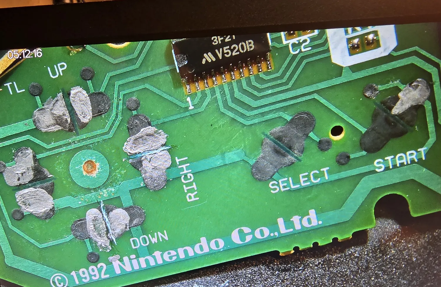
On conductive paint. When a carbon contact pad has genuinely worn through rather than just dirtied, paint is the repair of last resort and it does work. Clean first and be sure: isopropyl only, never an abrasive and never a fibreglass pen, because both strip the carbon layer permanently and turn a dirty pad into a worn one. If paint is warranted, keep it thin and off the surrounding traces: the patches above are thicker than I would like, and a blob that bridges to a neighbouring trace creates a stuck input. Replacement pad sets and silicone membranes are the tidier fix where they exist.
Chip and connector pinouts
The component library: each IC and connector defined once, with an interactive pin diagram where the package is drawable and a folded pin table underneath. The revision badge on each card shows which board or boards it applies to. The Nintendo ASICs carry only the handful of pins the mod literature actually names, because Nintendo never published a pinout for them.
Components & pinouts
Each part is defined once. The revision badge on every card shows exactly which board revision(s) it applies to.
Every diagram rotates and flips to match the board in front of you, zooms from a whole-package overview up to 3.2×, and saves at the orientation you are looking at — ↓ SVG matches the screen, and ↓ SVG (print) gives you the same drawing as ink on white. Both are vector, so print them at any size you like, which is the better route for the long connector pinouts since printing this page has to shrink them to fit the sheet. The # beside a part name links to that card, and the one in the pin panel links to a single pin — either link opens the card for whoever you send it to.
Audio RAM (32K × 8 pseudo-static) HM9453100FP, LH5P832N-12T/-12Y, MCM51L832AF10 SHVC-CPU-01 · SNS-CPU-GPM-01 · SNS-CPU-GPM-02 · SNS-CPU-RGB-01 · SNS-CPU-RGB-02 · SNSP-CPU-01 · SNSP-CPU-02 sop-28single sourceds-5p832,c5#
IC3/IC4 on the SHVC-SOUND module, U15/U16 on GPM through RGB-02 and both PAL multi-chip boards: 64 KB of APU RAM. Pin map is Sharp's LH5P832, the part on GPM-01, RGB-02 and the PAL boards.
Two 32K×8 parts make the 64 KB the S-DSP owns. They vanish from APU-01 onward because the S-APU swallows them, which is why an APU-01 or 1CHIP IC list jumps straight from U14 to U17 and then stops.
Why this is a separate entry from the video RAM. Console5 lists every RAM on a board in one bucket, and it is tempting to treat all of them as one jellybean. They are not. The parts observed in this position (Sharp’s LH5P832N, Motorola’s MCM51L832, the HM9453100FP) are true pseudo-static RAM: a DRAM array with on-chip refresh, not a static cell.
Where the table comes from, and what it covers. Sharp’s own LH5P832 datasheet, retrieved 2026-08-11, one part of the three. Sharp’s per-board position is Console5’s: LH5P832N-12T/-12Y on GPM-01, RGB-02 and both PAL boards. I still have no document for the Motorola MCM51L832 or the HM9453100FP (neither is indexed on datasheet4u, alldatasheet or datasheetarchive), so on an SHVC-CPU-01, RGB-01 or GPM-02 read the marking and treat this as the likely map rather than the confirmed one. The card stays tagged single-source for that reason.
The refresh pins are the part worth knowing. The footprint is the standard 28-pin 32K×8 one, and Sharp say so outright: the LH5P832 has “the same simple, non-multiplexed pinout as industry standard SRAMs” and will drop into a 32K×8 SRAM socket. The two differences from a 62256 are both on pins that already exist: 22 is OE/RFSH, not a plain /OE, and it is what clocks auto-refresh; 27 is R/W rather than /WE. There is also a self-refresh mode on an internal timer. So the danger with pasting the 62256 map across was never a pin count, it was reading pin 22 as an output enable and driving it accordingly.
Click a pin to see its signal, net, and sources.
Interactive diagram needs JavaScript. The full pinout is in the table below.
| Pin | Signal | Cat | Net | Note |
|---|---|---|---|---|
| 1 | A14 | bus | abus | ✓ |
| 2 | A12 | bus | abus | ✓ |
| 3 | A7 | bus | abus | ✓ |
| 4 | A6 | bus | abus | ✓ |
| 5 | A5 | bus | abus | ✓ |
| 6 | A4 | bus | abus | ✓ |
| 7 | A3 | bus | abus | ✓ |
| 8 | A2 | bus | abus | ✓ |
| 9 | A1 | bus | abus | ✓ |
| 10 | A0 | bus | abus | ✓ |
| 11 | I/O1 | bus | dbus | data bit 0 ✓ |
| 12 | I/O2 | bus | dbus | ✓ |
| 13 | I/O3 | bus | dbus | ✓ |
| 14 | GND | gnd | gnd | ground is pin 14, diagonally opposite VCC on 28 ✓ |
| 15 | I/O4 | bus | dbus | ✓ |
| 16 | I/O5 | bus | dbus | ✓ |
| 17 | I/O6 | bus | dbus | ✓ |
| 18 | I/O7 | bus | dbus | ✓ |
| 19 | I/O8 | bus | dbus | data bit 7 ✓ |
| 20 | /CE | signal | cs | chip enable, active low. A CE-only cycle also refreshes the addressed row. ✓ |
| 21 | A10 | bus | abus | the address line that breaks the run of control pins: 21 is NOT the write strobe ✓ |
| 22 | OE/RFSH | signal | oe | output enable AND the auto-refresh clock, both active low: the pin that is a plain /OE on a 62256. Each pulse refreshes the next row from the internal counter. ✓ |
| 23 | A11 | bus | abus | ✓ |
| 24 | A9 | bus | abus | ✓ |
| 25 | A8 | bus | abus | ✓ |
| 26 | A13 | bus | abus | ✓ |
| 27 | R/W | signal | we | read/write, write active low: Sharp's name for the pin a 62256 calls /WE ✓ |
| 28 | VCC | rail | vcc | +5 V ✓ |
CIC lockout chip (U8) F411 / F411A / F411B (NTSC), F419B (PAL multi-chip), F413B (PAL 1CHIP) SHVC-CPU-01 · SNS-CPU-GPM-01 · SNS-CPU-GPM-02 · SNS-CPU-RGB-01 · SNS-CPU-RGB-02 · SNS-CPU-APU-01 · SNS-CPU-1CHIP-01 · SNS-CPU-1CHIP-02 · SNS-CPU-1CHIP-03 · SNSP-CPU-01 · SNSP-CPU-02 · SNSP-CPU-1CHIP · SNN-CPU-01 sop-18✓sch-pal,snesdev-cic,cm-cic,cm-pins,borti#
18 pins, NOT 16: the 16-pin table on the superfamicom wiki is the cartridge-side numbering and will send you to the wrong pin
Naming: D prefix = through-hole (cartridges), F = surface-mount
(consoles); 411 = NTSC, 413 = PAL; a trailing letter is a revision. Console
parts observed: F411 on SHVC-CPU-01, F411A on the GPMs and RGB-01, F411B on
RGB-02 / APU-01 / all NTSC 1CHIP / SNN, F419B on the PAL multi-chip boards,
F413B on PAL 1CHIP.
The pin-count conflict, resolved. The superfamicom wiki prints a 16-pin CIC table with GND on 4 and Vcc on 16. The PAL schematic draws the console lock as an 18-pin device, ConsoleMods independently describes “a small 18-pin SMD chip in the vicinity of the reset button” with GND on 9, and the SNESdev wiki draws the same two devices side by side: a 16-pin DIP key chip for the cartridge and an 18-pin surface-mount lock chip for the console. That is what the 16-pin table actually is: the cart key, not the console lock. The pin numbers are silkscreened next to U8 anyway; read the silkscreen.
Why a lockout failure looks like dead silicon. If the handshake with the cartridge key fails, reset is never released on PPU2, so you get a black or solid-colour screen rather than any kind of lockout message. A dirty 62-pin connector produces exactly the same symptom.
Region-free is done by lifting pin 4 (it is strapped to +5 V for lock mode; grounding it makes the chip behave like a cart key). If you leave it lifted, tie it to ground (pin 9 is the convenient one) rather than floating it. On F41xB consoles you must also lift S-CLK pin 7. And ship a switch, not a permanent disable: SA-1 titles such as Super Mario RPG and Kirby Super Star detect a disabled CIC and refuse to boot.
Pin 11 is a reset output, not a data line. The PAL sheet labels it
P11 and routes it to cart pad 25, and it is tempting to read a port pin
going to the cartridge as the return data path. It is not. SNESdev names
it “/RESET for Cart CIC”, and its companion map of the 16-pin key chip
shows cart pad 25 landing on the key’s own RST input: the two agree. The
console lock therefore holds the cartridge key in reset on 11 and the
console in reset on 10, which is the same two-output arrangement the NES
CIC uses. The cart-to-console data actually rides pads 24 and 55, which
are pins 2 and 1 here.
Pins 5 and 12–17 are not connected, per SNESdev’s map: six unused pins in a row on the far side of the package. That is a useful bench fact: if you have continuity from any of them to anything, you are looking at a solder bridge, not a signal. It is one source, so they are tagged single-source; the PAL schematic simply leaves them undrawn, which is consistent but is not independent confirmation.
One conflict I have not resolved: the PAL sheet drives pin 6 as a second clock (CL2), while SNESdev marks pin 6 NC. I have kept the schematic’s reading because it is board-specific and drawn, not inferred, but treat pin 6 as the one entry in this table to meter before you trust it.
Click a pin to see its signal, net, and sources.
Interactive diagram needs JavaScript. The full pinout is in the table below.
| Pin | Signal | Cat | Net | Note |
|---|---|---|---|---|
| 1 | P00 / D2 (data out) | signal | cic_do1 | to cart pad 55: SNESdev calls this D2 ✓ |
| 2 | P01 / D1 (data out) | signal | cic_do2 | to cart pad 24: SNESdev calls this D1 ✓ |
| 3 | P02 / SEED | signal | podelay | to C62 (2.2 µF/50 V); SNESdev names it SEED, so the RC is the seed/power-on source rather than plain filtering ✓ |
| 4 | P03 (lock/key sel) | signal | lockmode | strapped to +5 V for lock mode; lift or ground it and the chip behaves like a cart key: this is the region-free pin ✓ |
| 5 | NC | nc | not connected single source | |
| 6 | CL2 (clock 2) | signal | cl2 | from U9 74HCU04 on NTSC, from S-CLK on PAL. SNESdev marks this pin NC: the one row in this table I would meter first. single source |
| 7 | CL1 (clock in) | signal | cl1 | borti taps this as Clk.CIC ✓ |
| 8 | RES (reset button) | signal | res_sw | active high at the chip; RESET_SW plus C29 100 nF ✓ |
| 9 | GND | gnd | gnd | ConsoleMods names this as the ground to tie a lifted pin 4 to ✓ |
| 10 | P10 (/RESET console) | signal | sysreset | the pin that actually holds the console in reset; borti drives /Rst.o here or at S-APU pin 100 ✓ |
| 11 | P11 (/RESET cart key) | signal | cic_keyrst | to cart pad 25: this RESETS the cartridge key, it is not the return data line. Cart data comes back on pads 24/55 = pins 2/1. ✓ |
| 12 | NC | nc | not connected single source | |
| 13 | NC | nc | not connected single source | |
| 14 | NC | nc | not connected single source | |
| 15 | NC | nc | not connected single source | |
| 16 | NC | nc | not connected single source | |
| 17 | NC | nc | not connected single source | |
| 18 | VCC | rail | vcc | +5 V, C85 100 nF ✓ |
AC power jack (PAL) PAL barrel jack: takes the same AC brick as the PAL NES (SNSP-002) SNSP-CPU-01 · SNSP-CPU-02 · SNSP-CPU-1CHIP header-2✓cm-diff,sfc-pin,sch-pal#
9 V AC, 1.3 A: rectified on the board, so this jack tolerates either polarity
A PAL SNES is not a DC console. It takes AC from the same adapter as the PAL NES and rectifies it on the board, which is why the jack does not care about polarity. SNSP-CPU-01/-02 use a bridge rectifier package; PAL 1CHIP boards use four discrete diodes instead, so a “missing bridge” on a PAL 1CHIP is normal.
Feeding a PAL unit 9 V DC half-works: the console runs, but the 12 V doubler that drives SCART auto-switching on multi-out pin 3 only reaches about 7.5 V, too low to trigger 4:3 switching.
Click a pin to see its signal, net, and sources.
Interactive diagram needs JavaScript. The full pinout is in the table below.
| Pin | Signal | Cat | Net | Note |
|---|---|---|---|---|
| 1 | AC in | rail | ac | 9 V AC: no polarity, on-board rectification ✓ |
| 2 | AC in | rail | ac | second AC leg bridge-ok ✓ |
Cartridge slot (62-pin) 62-pin Nintendo edge connector: more than one physical type across revisions SHVC-CPU-01 · SNS-CPU-GPM-01 · SNS-CPU-GPM-02 · SNS-CPU-RGB-01 · SNS-CPU-RGB-02 · SNS-CPU-APU-01 · SNS-CPU-1CHIP-01 · SNS-CPU-1CHIP-02 · SNS-CPU-1CHIP-03 · SNSP-CPU-01 · SNSP-CPU-02 · SNSP-CPU-1CHIP · SNN-CPU-01 edge-62✓sfc-pin,cm-pins,sch-ntsc#
identical pinout in every region: only the shell shape and the slot tabs differ. Pins 1–31 front row, 32–62 rear.
Two independent pinouts (the superfamicom wiki and ConsoleMods) agree across the whole connector, which is why this card is verified. Two differences in how they present it, both resolved below:
- Pins 41–48 are the bank-address byte. The superfamicom wiki calls them A16–A23; ConsoleMods calls them BA0–BA7. Same lines, different naming.
- ConsoleMods’ table prints “D3” at pin 23; that is a typo, pin 23 is /RD. The superfamicom wiki, the schematic and ConsoleMods’ own pin 54 (/WR) all agree.
Pins 1–4, 28–35 and 59–62 are split off from the main run and are used only by cartridges with enhancement chips. That is why I test every unit with a Super FX or SA-1 cartridge before listing it: those are the only carts that touch the outer groups and the only ones that load the +5 V rail hard, so a board that is marginal will pass a Super Mario World smoke test and fail for the buyer.
Nintendo’s service literature makes this connector the number-one probable cause for solid-colour, scrambled and frozen screens, and then says not to clean it, but to replace it. I do not agree with the second half; see the replacement-parts table.
Click a pin to see its signal, net, and sources.
Interactive diagram needs JavaScript. The full pinout is in the table below.
| Pin | Signal | Cat | Net | Note |
|---|---|---|---|---|
| 1 | Master clock | signal | clk | 21.477 MHz NTSC, buffered off the X1 oscillator ✓ |
| 2 | /EXPAND | signal | expand | ties to expansion-port pin 24 ✓ |
| 3 | PA6 | bus | babus | B-address bus ✓ |
| 4 | /PARD | signal | pard | B-bus read strobe ✓ |
| 5 | GND | gnd | gnd | bridge-ok ✓ |
| 6 | A11 | bus | abus | ✓ |
| 7 | A10 | bus | abus | ✓ |
| 8 | A9 | bus | abus | ✓ |
| 9 | A8 | bus | abus | ✓ |
| 10 | A7 | bus | abus | ✓ |
| 11 | A6 | bus | abus | ✓ |
| 12 | A5 | bus | abus | ✓ |
| 13 | A4 | bus | abus | ✓ |
| 14 | A3 | bus | abus | ✓ |
| 15 | A2 | bus | abus | ✓ |
| 16 | A1 | bus | abus | ✓ |
| 17 | A0 | bus | abus | ✓ |
| 18 | /IRQ | signal | irq | bidirectional: the cart can assert it ✓ |
| 19 | D0 | bus | dbus | ✓ |
| 20 | D1 | bus | dbus | ✓ |
| 21 | D2 | bus | dbus | ✓ |
| 22 | D3 | bus | dbus | ✓ |
| 23 | /RD | signal | rd | read strobe: ConsoleMods' table mislabels this pin 'D3' ✓ |
| 24 | CIC data out | signal | cic_do2 | from CIC pin 2 ✓ |
| 25 | CIC data in | signal | cic_di | to CIC pin 11 ✓ |
| 26 | /RESET | signal | reset | active low; the cart may also pull it ✓ |
| 27 | Vcc +5 V | rail | vcc | bridge-ok ✓ |
| 28 | PA0 | bus | babus | expansion-chip carts only ✓ |
| 29 | PA2 | bus | babus | expansion-chip carts only ✓ |
| 30 | PA4 | bus | babus | expansion-chip carts only ✓ |
| 31 | Left audio in | signal | audio_l | cartridge audio, mixed into the APU output ✓ |
| 32 | /WRAM | signal | wram | low while the CPU is accessing work RAM ✓ |
| 33 | REFRESH | signal | refresh | RAM refresh, roughly 40 master cycles per scanline ✓ |
| 34 | PA7 | bus | babus | ✓ |
| 35 | /PAWR | signal | pawr | B-bus write strobe ✓ |
| 36 | GND | gnd | gnd | bridge-ok ✓ |
| 37 | A12 | bus | abus | ✓ |
| 38 | A13 | bus | abus | ✓ |
| 39 | A14 | bus | abus | ✓ |
| 40 | A15 | bus | abus | ✓ |
| 41 | A16 (BA0) | bus | abus | bank byte: ConsoleMods calls 41–48 BA0–BA7 ✓ |
| 42 | A17 (BA1) | bus | abus | ✓ |
| 43 | A18 (BA2) | bus | abus | ✓ |
| 44 | A19 (BA3) | bus | abus | ✓ |
| 45 | A20 (BA4) | bus | abus | ✓ |
| 46 | A21 (BA5) | bus | abus | ✓ |
| 47 | A22 (BA6) | bus | abus | ✓ |
| 48 | A23 (BA7) | bus | abus | ✓ |
| 49 | /CART | signal | romsel | also called /ROMSEL: low on a ROM access ✓ |
| 50 | D4 | bus | dbus | ✓ |
| 51 | D5 | bus | dbus | ✓ |
| 52 | D6 | bus | dbus | ✓ |
| 53 | D7 | bus | dbus | ✓ |
| 54 | /WR | signal | wr | write strobe ✓ |
| 55 | CIC data out | signal | cic_do1 | from CIC pin 1 ✓ |
| 56 | CIC clock out | signal | cicclk | buffered from U9 pin 2 on NTSC, from S-CLK pin 7 on PAL multi-chip ✓ |
| 57 | CPU clock | signal | cpuclk | 6, 8 or 12 master cycles per cycle: 3.58 / 2.68 / 1.79 MHz ✓ |
| 58 | Vcc +5 V | rail | vcc | bridge-ok ✓ |
| 59 | PA1 | bus | babus | expansion-chip carts only ✓ |
| 60 | PA3 | bus | babus | expansion-chip carts only ✓ |
| 61 | PA5 | bus | babus | expansion-chip carts only ✓ |
| 62 | Right audio in | signal | audio_r | cartridge audio, mixed into the APU output ✓ |
Controller port (7-pin) 7-pin Nintendo controller socket SHVC-CPU-01 · SNS-CPU-GPM-01 · SNS-CPU-GPM-02 · SNS-CPU-RGB-01 · SNS-CPU-RGB-02 · SNS-CPU-APU-01 · SNS-CPU-1CHIP-01 · SNS-CPU-1CHIP-02 · SNS-CPU-1CHIP-03 · SNSP-CPU-01 · SNSP-CPU-02 · SNSP-CPU-1CHIP · SNN-CPU-01 header-7✓sfc-pin,cm-pins#
same on every revision. Pins 1–4 sit in the square part of the shell, 5–7 in the rounded part.
Both sources agree on the four wires a standard pad actually uses, and the OEM wire colours are the fastest way to check a controller cable: white +5 V, yellow clock, orange latch, red data, brown ground.
Pins 5 and 6 are where the two tables read differently and it is worth
knowing why. ConsoleMods lists them N/C because a standard controller has
no wires there. The superfamicom wiki names them from the console side:
Data2 (a second data line, used by splitters and multitaps) and IOBit
(wired to the I/O port at $4201/$4213). Both are correct from their own
end; the console-side names are the useful ones on a bench.
Anything plugged into port 2 can latch the H and V counters by pulling its IOBit low, because port 2’s IOBit is bit 7 of the I/O port and that bit is tied to the PPU counter latch.
Click a pin to see its signal, net, and sources.
Interactive diagram needs JavaScript. The full pinout is in the table below.
| Pin | Signal | Cat | Net | Note |
|---|---|---|---|---|
| 1 | +5 V | rail | v5 | white wire ✓ |
| 2 | Clock | signal | clock | yellow wire; port 1 clocks on reads of $4016, port 2 on $4017 ✓ |
| 3 | Latch | signal | latch | orange wire; written through bit 0 of $4016 ✓ |
| 4 | Data1 | signal | data1 | red wire; read through bit 0 of $4016/$4017. Pulled low inside the console, so an empty port reads 0. ✓ |
| 5 | Data2 | signal | data2 | second data line: unused by a standard pad, used by splitters/multitaps. ConsoleMods lists it N/C from the controller end. ✓ |
| 6 | IOBit | signal | iobit | to the I/O port ($4201/$4213); port 1 = bit 6, port 2 = bit 7 (which also latches the PPU counters) single source |
| 7 | Ground | gnd | gnd | brown wire ✓ |
Controller cable connector (P1, "SHVC SP") 5-way header inside the controller shell SHVC-001 controller header-5✓oem-tech#
the pad end of the cable: five conductors, matching the four wires a standard pad uses plus ground
The controller has no regulator of its own: VDD and VSS come straight from the console through this cable, so every logic level in the pad swings 0 to 5 V. A healthy console reads roughly 4.75 to 5.1 V here; meaningfully lower points at the console’s regulator rather than the pad.
Maps onto the console’s 7-pin port as 1-to-7, 2-to-4, 3-to-3, 4-to-2, 5-to-1: see the controller-port card for the wire colours.
Click a pin to see its signal, net, and sources.
Interactive diagram needs JavaScript. The full pinout is in the table below.
| Pin | Signal | Cat | Net | Note |
|---|---|---|---|---|
| 1 | VSS | gnd | gnd | ground; console port pin 7, brown wire ✓ |
| 2 | Q (4016D0) | signal | data1 | serial data to the console; port pin 4, red wire. The label names its destination: bit 0 of $4016. ✓ |
| 3 | P/S (OUT0) | signal | latch | latch; port pin 3, orange wire ✓ |
| 4 | CLOCK (CPU) | signal | clock | clock; port pin 2, yellow wire ✓ |
| 5 | VDD | rail | v5 | +5 V; port pin 1, white wire ✓ |
DC power jack (NTSC / JP) NA: Nintendo-specific keyed barrel with an inner pin. SFC / Super Comboy: 5.5 × 2.1 mm barrel. SHVC-CPU-01 · SNS-CPU-GPM-01 · SNS-CPU-GPM-02 · SNS-CPU-RGB-01 · SNS-CPU-RGB-02 · SNS-CPU-APU-01 · SNS-CPU-1CHIP-01 · SNS-CPU-1CHIP-02 · SNS-CPU-1CHIP-03 · SNN-CPU-01 header-2✓oem-tech,sfc-pin,cm-diff,sch-ntsc#
10 V DC, 850 mA, unregulated, CENTRE-NEGATIVE. Meter an unknown brick before you plug it in.
Centre-negative is the detail that kills consoles. The OEM manual gives 10 V DC unregulated; the superfamicom wiki and the SNS-002 / HVC-002 adapter labels give 850 mA and the polarity. You will see 9 V quoted in places: the OEM figure is 10 V, and anything from 9 to 10 V DC centre-negative is safe.
The jacks are keyed, not electrically different: the Super Famicom and Korean Super Comboy use the Famicom’s 5.5 × 2.1 mm barrel, while the North American jack has an inner pin specifically so a 9 V AC NES brick cannot be inserted. A generic 5.5 × 2.5 mm barrel is NOT a drop-in for a US deck.
The community’s reported number-one no-power cause is this part: the centre post fatigues and cracks its joint. Reflow first, replace if the post is loose.
The mounting also has a switch lug on some variants that I have not mapped; the two pins below are the electrical input pair.
Click a pin to see its signal, net, and sources.
Interactive diagram needs JavaScript. The full pinout is in the table below.
| Pin | Signal | Cat | Net | Note |
|---|---|---|---|---|
| 1 | Centre (tip) | gnd | gnd | 0 V: the SNES adapter is centre-NEGATIVE ✓ |
| 2 | Sleeve | rail | vin | +10 V DC nominal, unregulated, into the choke → fuse → series diode → reservoir chain ✓ |
EXT expansion port (28-pin, bottom) 28-pin bottom expansion connector (Satellaview) SHVC-CPU-01 · SNS-CPU-GPM-01 · SNS-CPU-GPM-02 · SNS-CPU-RGB-01 · SNS-CPU-RGB-02 · SNS-CPU-APU-01 · SNS-CPU-1CHIP-01 · SNS-CPU-1CHIP-02 · SNS-CPU-1CHIP-03 · SNSP-CPU-01 · SNSP-CPU-02 · SNSP-CPU-1CHIP edge-28✓sfc-pin,cm-pins#
under the door on the bottom of an original (001) console. The New-Style / Jr deletes it entirely.
Two independent pinouts agree, so this card is verified. The B-address bus, the data bus, reset and IRQ all appear here, plus two clocks and the audio mix.
Orientation: hold the console upside down with the controller ports facing you and pin 1 is the lower right, pin 28 the upper left. The list below is numerical, not spatial: the physical connector pairs odd and even pins across from each other.
The port’s absence is a fast 001-vs-101 identification tell: pull the door on the bottom of an original console and you find this; a New-Style / Jr has no bottom port at all. On PAL originals the area behind the door is also a 1CHIP tell: a 1CHIP shows a plain solder ring where a multi-chip board shows a dot pattern.
Click a pin to see its signal, net, and sources.
Interactive diagram needs JavaScript. The full pinout is in the table below.
| Pin | Signal | Cat | Net | Note |
|---|---|---|---|---|
| 1 | PA0 | bus | babus | ✓ |
| 2 | PA1 | bus | babus | ✓ |
| 3 | PA2 | bus | babus | ✓ |
| 4 | PA3 | bus | babus | ✓ |
| 5 | PA4 | bus | babus | ✓ |
| 6 | PA5 | bus | babus | ✓ |
| 7 | PA6 | bus | babus | ✓ |
| 8 | PA7 | bus | babus | ✓ |
| 9 | /PAWR | signal | pawr | B-bus write ✓ |
| 10 | /PARD | signal | pard | B-bus read ✓ |
| 11 | D0 | bus | dbus | ✓ |
| 12 | D1 | bus | dbus | ✓ |
| 13 | D2 | bus | dbus | ✓ |
| 14 | D3 | bus | dbus | ✓ |
| 15 | D4 | bus | dbus | ✓ |
| 16 | D5 | bus | dbus | ✓ |
| 17 | D6 | bus | dbus | ✓ |
| 18 | D7 | bus | dbus | ✓ |
| 19 | /RESET | signal | reset | the attached device can also assert it ✓ |
| 20 | Vcc | rail | vcc | +5 V ✓ |
| 21 | SMPCLK | signal | smpclk | audio sample clock, about 8.192 MHz ✓ |
| 22 | DOTCLK | signal | dotclk | PPU2 dot clock, about 5.369 MHz (21.477/4) ✓ |
| 23 | GND | gnd | gnd | ✓ |
| 24 | EXPAND | signal | expand | to cart pin 2 ✓ |
| 25 | MONO-OUT | signal | mono | mono audio taken AFTER the mix ✓ |
| 26 | /IRQ | signal | irq | bidirectional ✓ |
| 27 | Left audio in | signal | audio_l | mixed into the APU output, same as cart pin 31 ✓ |
| 28 | Right audio in | signal | audio_r | mixed into the APU output, same as cart pin 62 ✓ |
Front controller-board harness (P2 / FFC) flat cable + connector between the mainboard and the front controller PCB SHVC-CPU-01 · SNS-CPU-GPM-01 · SNS-CPU-GPM-02 · SNS-CPU-RGB-01 · SNS-CPU-RGB-02 · SNS-CPU-APU-01 · SNS-CPU-1CHIP-01 · SNS-CPU-1CHIP-02 · SNS-CPU-1CHIP-03 · SNSP-CPU-01 · SNSP-CPU-02 · SNSP-CPU-1CHIP · SNN-CPU-01 ffcsingle sourceborti,c5,oem-tech#
three contacts named by the mod literature: 6/8/10 are controller 1's data, clock and latch. The rest of the cable is unmapped.
Worth naming because it is the first thing to check when one or both controller ports go intermittent, and it is easy to disturb during a shell swap or a retrobright. Nintendo’s own order is the front unit PCB, then the FFC harness, then connector P2, then the CPU.
What is actually documented. borti’s MultiRegion install notes name three contacts on this cable, because the mod board sniffs controller 1 through them: pin 10 is the latch (controller pin 3), pin 8 the clock (controller pin 2), pin 6 the serial data (controller pin 4). Those are the ones a region-switch install lands on, so they are the three worth knowing. Every other contact (the second port’s lines, IOBit, +5 V and ground) is unmapped in every source I hold, and I have not assigned them numbers on inference.
The odd numbering (6, 8, 10 with gaps) reads like alternating signal/ground on the ribbon, which would be a sensible way to build it, but that is a guess and I have not metered it. Settling this properly takes one board: ring each contact out to the two controller jacks and the cable is done, pin count and all. Until then the package pin count stays at 0.
| Pin | Signal | Cat | Net | Note |
|---|---|---|---|---|
| 6 | Data1 (port 1) | signal | p1data | serial data from controller 1: equivalent to controller connector pin 4 single source |
| 8 | Clock (port 1) | signal | p1clk | data clock for controller 1: equivalent to controller connector pin 2 single source |
| 10 | Latch (port 1) | signal | p1latch | data latch for controller 1: equivalent to controller connector pin 3 single source |
A/V Multi Out (12-pin) Nintendo Multi Out SHVC-CPU-01 · SNS-CPU-GPM-01 · SNS-CPU-GPM-02 · SNS-CPU-RGB-01 · SNS-CPU-RGB-02 · SNS-CPU-APU-01 · SNS-CPU-1CHIP-01 · SNS-CPU-1CHIP-02 · SNS-CPU-1CHIP-03 · SNSP-CPU-01 · SNSP-CPU-02 · SNSP-CPU-1CHIP · SNN-CPU-01 header-12✓sfc-pin,sch-c5,sch-pal,cm-video,rgb-csync#
PIN 3 IS THE HAZARD: composite sync on NTSC, +12 V on PAL. Physically the odd pins are one row and the even pins the other.
Read this before you plug a cable in. On a PAL SNES, pin 3 carries the
+12 V zener rail used for SCART auto-switching, where an NTSC unit puts a
TTL composite-sync signal. The PAL schematic literally names the multi-out
pin 3 net +12V. Connecting an NTSC CSYNC cable to a PAL console can damage
downstream equipment. On PAL, take sync from luma (pin 7) or composite
(pin 9). If you fit a dejitter or RGB-amp board that drives csync onto pin
3 of a PAL unit, the +12 V feed has to come off first.
A related non-fault: if a PAL unit “stopped switching the TV to 4:3”, suspect a DC supply. The 12 V comes from a doubler that only reaches 12 V on a true AC input and sits near 7.5 V on DC: too low to trigger the switch.
Levels, from the OEM sheet: RGB and Y/C are labelled 1 Vpp into 75 Ω with about 1 V of DC offset; sync and composite are labelled 5 Vpp, which is an open-circuit drive figure: marqs85 measured the identical driver at about 2.5 Vpp unterminated and 1.1 Vpp into 75 Ω. Do not expect 5 Vpp at a terminated input.
Two board-specific gaps: SNS-CPU-1CHIP-03 ships with the csync driver depopulated (the only original NTSC console with no csync here), and SNN-CPU-01 never had S-video routed to pins 7/8 even though Y/C exists at the encoder. Both are covered in the parts table.
The diagram below draws the twelve pins as one row for legibility; the real connector is two staggered rows, odd pins together and even pins together.
One older copy of the superfamicom table describes pins 11/12 as “mid (L+R)” and “side (L−R)” sound. The second table on the same page, the schematics and every cable pinout say plain left and right, which is what I have used.
Click a pin to see its signal, net, and sources.
Interactive diagram needs JavaScript. The full pinout is in the table below.
| Pin | Signal | Cat | Net | Note |
|---|---|---|---|---|
| 1 | Red | signal | red | 1 Vpp into 75 Ω, ~1 V DC offset ✓ |
| 2 | Green | signal | green | ✓ |
| 3 | CSYNC / +12 V (PAL) | signal | csync | NTSC: TTL composite sync. PAL: +12 V SCART switching rail. An NTSC csync cable here can damage gear. ✓ |
| 4 | Blue | signal | blue | ✓ |
| 5 | Ground | gnd | gnd | bridge-ok ✓ |
| 6 | Ground | gnd | gnd | bridge-ok ✓ |
| 7 | Y (luma) | signal | luma | S-video luma; not routed from the factory on SNN-CPU-01 ✓ |
| 8 | C (chroma) | signal | chroma | S-video chroma; not routed from the factory on SNN-CPU-01 ✓ |
| 9 | CVBS | signal | cvbs | composite video, 1 Vpp into 75 Ω ✓ |
| 10 | Vcc +5 V | rail | v5 | powers an external RF modulator / reads as a logic high ✓ |
| 11 | Audio L | signal | audio_l | line level, out of the U10 stage ✓ |
| 12 | Audio R | signal | audio_r | line level, out of the U10 stage ✓ |
SHVC-SOUND module connector (P5) plug-on audio daughtercard connector: SHVC-CPU-01 only SHVC-CPU-01 headerbenchc5,oem-tech,bench#
the only detachable audio section Nintendo ever shipped on this platform: pin count and pinout not published anywhere I have
SHVC-CPU-01 is the one revision where the whole sound section (S-SMP, S-DSP, audio RAM, DAC and output amp) plugs on as the SHVC-SOUND daughtercard. Nintendo’s distorted-or-no-sound tree ranks this connector, P5, second: right after the module itself.
On one of these boards I check the module FIRST: present, fully seated, clean contacts. A bad connection or a bad module either stops the console working at all or crashes it the instant a game initialises sound, so this is the one board where reseating and cleaning an audio module is a real, cheap first move. Every other revision has the audio soldered down.
I have not found a published pin count or pinout for P5 in any source. The two full SNES schematics I hold both draw the audio section soldered inline, because both are drawn from a later board, so neither shows this connector at all, and there is nothing here to publish. Ringing the SHVC-SOUND module’s edge contacts out against the mainboard would settle it in one sitting, and that is the only route I can see to a real pinout.
No pins captured yet — bench stub.
Reset / CIC glue inverter (U9) 74HCU04 unbuffered hex inverter SHVC-CPU-01 · SNS-CPU-GPM-01 · SNS-CPU-GPM-02 · SNS-CPU-RGB-01 · SNS-CPU-RGB-02 · SNS-CPU-APU-01 · SNSP-CPU-01 · SNSP-CPU-02 sop✓c5,oem-tech,cm-pins,sch-c5#
multi-chip boards only: on 1CHIP and Jr, U9 is the 7805 instead. Third in Nintendo's no-reset tree.
An unbuffered hex inverter used as the CIC clock oscillator on NTSC boards (with R72 1 MΩ and C55/C56 around it) and as reset glue. Nintendo’s no-reset priority runs CIC → X2 4 MHz oscillator → this chip.
Only one pin is mapped in my sources: ConsoleMods traces cart pad 56, the CIC clock the cartridge sees, back to pin 2 of U9. I have not filled the rest, and I am not assuming a package pin count on the strength of “hex inverters are usually 14-pin”.
| Pin | Signal | Cat | Net | Note |
|---|---|---|---|---|
| 2 | CIC clock out | signal | cicclk | buffered CIC clock to cart pad 56 single source |
Controller shift register: 56V520 (single-IC pad) Nintendo 56V520: 14-bit parallel-in / serial-out shift register SHVC-001 controller dip-20✓oem-tech#
the single-IC controller variant; a Nintendo house part, NOT a jellybean: no 4021 or other logic-family substitute exists
Nintendo built the SNES pad two ways and the service manual documents both. This is the one-chip version: a single 14-bit shift register, of which twelve parallel inputs go to the carbon contact pads and two are spare. There is no drop-in replacement (a 4021 is 8-bit, and nothing common gives you 14 stages in one package), so a dead one means a donor pad.
Read the pin numbering carefully: the parallel inputs are scattered around the package for PCB routing convenience, so PI 9 lands on pin 1 and PI 1 on pin 6. The order carries no logical meaning.
Which button lands on which PI input is NOT captured here: the twelve contact lines cross each other on the schematic and I have not traced them individually. The pin numbers below are read directly off the drawing and every number 1 through 20 appears exactly once, which is the internal check that the transcription is complete.
Click a pin to see its signal, net, and sources.
Interactive diagram needs JavaScript. The full pinout is in the table below.
| Pin | Signal | Cat | Net | Note |
|---|---|---|---|---|
| 1 | PI 9 | signal | pi9 | ✓ |
| 2 | PI 8 | signal | pi8 | ✓ |
| 3 | PI 7 | signal | pi7 | ✓ |
| 4 | PI 12 | signal | pi12 | ✓ |
| 5 | PI 11 | signal | pi11 | ✓ |
| 6 | PI 1 | signal | pi1 | ✓ |
| 7 | CLK | signal | clk | clock from the console, port pin 2 ✓ |
| 8 | P/S | signal | ps | parallel/serial load: the latch, port pin 3 ✓ |
| 9 | Q14 | signal | q14 | serial data out to the console, port pin 4 ✓ |
| 10 | VSS | gnd | gnd | ground, 0 V ✓ |
| 11 | D IN | signal | din | serial input; tied to ground in the single-IC pad ✓ |
| 12 | PI 2 | signal | pi2 | ✓ |
| 13 | PI 13 | signal | pi13 | ✓ |
| 14 | PI 14 | signal | pi14 | ✓ |
| 15 | PI 6 | signal | pi6 | ✓ |
| 16 | PI 5 | signal | pi5 | ✓ |
| 17 | PI 3 | signal | pi3 | ✓ |
| 18 | PI 4 | signal | pi4 | ✓ |
| 19 | PI 10 | signal | pi10 | ✓ |
| 20 | VDD | rail | v5 | +5 V from the console, port pin 1 ✓ |
Controller shift register: 56W545 (dual-IC pad) Nintendo 56W545: 8-bit parallel-in / serial-out shift register, two per controller SHVC-001 controller dip-14✓oem-tech#
the two-chip controller variant: IC-A and IC-B cascaded; also a Nintendo house part with no jellybean equivalent
The other way Nintendo built the pad: two 8-bit shift registers in series. IC-B’s Q8 feeds IC-A’s D IN, and IC-A’s Q8 goes to the console, so the console clocks twelve bits out of what is physically a sixteen-stage chain.
The button map here IS captured, because this drawing routes cleanly, and it corroborates the documented SNES report order exactly. Data shifts toward Q8, so the highest-numbered input comes out first:
- IC-A, PI 1 to PI 8 = Right, Left, Down, Up, Start, Select, Y, B
- IC-B, PI 5 to PI 8 = R, L, X, A (PI 1 to PI 4 unused)
Shifting out from PI 8 downward gives B, Y, Select, Start, Up, Down, Left, Right from IC-A and then A, X, L, R from IC-B, which is the standard twelve-bit SNES controller order that software expects. Two independent supports: the drawing itself, and the protocol.
Click a pin to see its signal, net, and sources.
Interactive diagram needs JavaScript. The full pinout is in the table below.
| Pin | Signal | Cat | Net | Note |
|---|---|---|---|---|
| 1 | PI 8 | signal | pi8 | IC-A: B / IC-B: A ✓ |
| 2 | Q8 | signal | q8 | serial out; IC-A to the console, IC-B into IC-A's D IN ✓ |
| 3 | PI 4 | signal | pi4 | IC-A: Up ✓ |
| 4 | PI 3 | signal | pi3 | IC-A: Down ✓ |
| 5 | PI 2 | signal | pi2 | IC-A: Left ✓ |
| 6 | PI 1 | signal | pi1 | IC-A: Right ✓ |
| 7 | VSS | gnd | gnd | ground, 0 V ✓ |
| 8 | P/S | signal | ps | parallel/serial load: the latch ✓ |
| 9 | CLK | signal | clk | clock from the console ✓ |
| 10 | D IN | signal | din | serial input; IC-A takes IC-B's Q8 here ✓ |
| 11 | PI 5 | signal | pi5 | IC-A: Start / IC-B: R ✓ |
| 12 | PI 6 | signal | pi6 | IC-A: Select / IC-B: L ✓ |
| 13 | PI 7 | signal | pi7 | IC-A: Y / IC-B: X ✓ |
| 14 | VDD | rail | v5 | +5 V from the console ✓ |
Reset generator / voltage supervisor (U11) Mitsumi PST529D: marked T529D SHVC-CPU-01 · SNS-CPU-GPM-01 · SNS-CPU-GPM-02 · SNS-CPU-RGB-01 · SNS-CPU-RGB-02 · SNS-CPU-APU-01 · SNS-CPU-1CHIP-01 · SNS-CPU-1CHIP-02 · SNS-CPU-1CHIP-03 · SNSP-CPU-01 · SNSP-CPU-02 · SNSP-CPU-1CHIP✓ds-pst529,c5,oem-tech,sch-c5#
three pins: 1 VCC, 2 GND, 3 open-collector reset out. Present on every board EXCEPT SNN-CPU-01 (the Jr has no U11): a real revision tell.
A low-voltage detector that watches +5 V and drives the system RST node through R75 (100 kΩ), holding the console in reset through brownouts so WRAM and cartridge SRAM writes are not corrupted. RST reaches the S-CPU, the work RAM, and cart pin 26.
The marking decodes. Mitsumi’s PST529 series datasheet photographs a
part marked T529C, which settles the convention: the T529D on the
board is a PST529D. The suffix is the trip point, and the sheet’s
table gives D as 4.0 / 4.2 / 4.4 V min/typ/max detecting voltage, with
50 mV typical hysteresis. So this part releases reset at about 4.2 V on a
5 V rail: if you are chasing a console that boots to black on a sagging
supply, that is the number to measure against.
Pin 3 is open-collector. The datasheet specs it as a low-level output voltage with a leakage current at Vcc = 15 V, and its applied circuit draws an external pull-up plus a capacitor to set the power-on delay. That is exactly what R75 does here, so do not expect to see the part actively drive RST high: it lets go and the pull-up does the rest. A stuck-low RST is either this part or CIC pin 10.
On the package. The Mitsumi databook I have only draws a 3-lead
through-hole plastic package; Mitsumi also catalogued SMD MT variants of
the same series. I have not confirmed which one Nintendo fitted at U11, so
I have not asserted a package type here: only the pin count and the pin
functions, which the equivalent circuit and the applied circuit both give
as 1 VCC / 2 GND / 3 Out.
Console5’s per-board IC lists show U11 on every revision except SNN-CPU-01, so an empty U11 position on a Jr is factory, not a missing part. (Console5’s GPM-02 list also omits U11, which I read as a transcription gap rather than a design change, since it is present either side.)
| Pin | Signal | Cat | Net | Note |
|---|---|---|---|---|
| 1 | VCC | rail | v5 | +5 V: this is both the supply and the rail being watched ✓ |
| 2 | GND | gnd | gnd | ✓ |
| 3 | Reset out | signal | rst | open-collector, pulled low while VCC is below the trip point; R75 (100 kΩ) is the external pull-up that makes it a usable RST ✓ |
+5 V linear regulator 7805 (TO-220): U12 on multi-chip, U9 on 1CHIP and Jr SHVC-CPU-01 · SNS-CPU-GPM-01 · SNS-CPU-GPM-02 · SNS-CPU-RGB-01 · SNS-CPU-RGB-02 · SNS-CPU-APU-01 · SNS-CPU-1CHIP-01 · SNS-CPU-1CHIP-02 · SNS-CPU-1CHIP-03 · SNSP-CPU-01 · SNSP-CPU-02 · SNSP-CPU-1CHIP · SNN-CPU-01 to-220-3single sourcec5,sch-ntsc,sch-pal#
on the heatsink; runs hot by design dropping ~10 V to 5 V. Keep it linear if you replace it.
Standard three-terminal 78xx orientation: input, ground, output. I am tagging this single-source because I read the terminal order off Console5’s own vertical-line instruction (“stripe on the centre terminal, non-striped side on the output, right side”) rather than off a 78xx datasheet in my own files.
Two things worth saying about this part. It runs hot by design: that is not a fault. And it is fourth in Nintendo’s no-power tree, after F1, D1 and the T1 line filter.
If you replace it, keep it linear. Switching drop-in modules run cool but can inject rolling lines into the picture. And do not follow the general retro advice about feeding the regulator a lower input to cut heat: this is not a 5 V-only console, because the raw input rail also feeds the video and audio buffers through the Q18 emitter follower.
| Pin | Signal | Cat | Net | Note |
|---|---|---|---|---|
| 1 | IN | rail | vin | raw rail from the fuse/rectifier side single source |
| 2 | GND | gnd | gnd | centre terminal: the vertical-line 470 µF goes negative-stripe here single source |
| 3 | OUT | rail | v5 | +5.0 V, the only regulated logic rail single source |
S-APU (fused audio processor) S-APU: S-SMP + S-DSP + sound RAM in one package SNS-CPU-APU-01 · SNS-CPU-1CHIP-01 · SNS-CPU-1CHIP-02 · SNS-CPU-1CHIP-03 · SNSP-CPU-1CHIP · SNN-CPU-01 qfp✓cm-diff,c5,borti#
U13 on APU-01, U2 on every 1CHIP and Jr board; deletes U15–U17 (audio PSRAM + DAC positions move)
The fusion that ends the multi-chip audio section: S-SMP, S-DSP and the two audio PSRAMs collapse into one package. On APU-01 the DAC then moves up to U14; on 1CHIP and Jr boards it is U6.
The one pin the mod literature names is 100, the APU reset: borti’s
multiregion board wires its /Rst.o either here or to CIC pin 10.
The schematics do not help here either. S-APU first appears on SNS-CPU-APU-01, and neither full-board drawing I hold reaches that far: the NTSC sheet stops at RGB-02 and the PAL sheet is a multi-chip SNSP board. There is no S-APU symbol on either, so this stays a stub. The separate S-SMP and S-DSP entries have full maps, but this part fuses them with the sound RAM into one package and renumbers everything; nothing carries across.
| Pin | Signal | Cat | Net | Note |
|---|---|---|---|---|
| 100 | APU /RESET | signal | reset | reset input; borti's multiregion board drives it here as an alternative to CIC pin 10 single source |
S-CLK clock multiplier (PAL multi-chip only) S-CLK / S-CLK A (U18) SNSP-CPU-01 · SNSP-CPU-02 sop-14✓sch-pal,c5,borti,cm-cic#
makes the ~21.281 MHz master clock from a 17.734475 MHz crystal (×6/5); exists ONLY on PAL multi-chip boards
The part that makes PAL region conversion different from NTSC. A PAL multi-chip board does not run a 21 MHz crystal: X1 is 17.734475 MHz (four times the PAL colour subcarrier) and this chip multiplies it by 6/5. Drop an NTSC crystal in and the multiplier takes the system clock to about 25.77 MHz and the console will not boot.
PAL 1CHIP boards and the Jr do the same multiply inside the S-CPUN, which is precisely why no S-CLK appears in their IC lists.
It also carries a late-revision CIC gotcha: on F41xB consoles, lifting CIC pin 4 alone is not enough for region-free. Pin 7 here must be lifted too, and re-enabling wants a DPDT that returns CIC pin 4 to +5 V and this pin 7 to cart pin 56.
The pin count is on the PAL sheet after all: the symbol is numbered 1–14, seven contacts a side. I had previously left it uncounted; that was my error, not the drawing’s. What the drawing does not give is a name for pins 8, 9, 11, 12 and 13, which are drawn but unlabelled, so those are absent from the table below. Pin 14 is labelled “+5V?” (with the author’s own question mark), so I have left it out too.
Click a pin to see its signal, net, and sources.
Interactive diagram needs JavaScript. The full pinout is in the table below.
| Pin | Signal | Cat | Net | Note |
|---|---|---|---|---|
| 1 | XIN (crystal) | signal | xtal | X1 17.734475 MHz; R73 (0 Ω) sits in the XIN path single source |
| 2 | Crystal | signal | xtal | second crystal terminal single source |
| 3 | +5V | rail | vcc | single source |
| 4 | XOUT (master) | signal | master | ≈21.281 MHz: this, not the crystal, is the board master clock ✓ |
| 5 | 4.433 MHz | signal | cc_pal | PAL colour carrier to the encoder; also borti's colour-carrier tap on PAL single source |
| 6 | 3.546 MHz | signal | cc_alt | single source |
| 7 | CIC clock out | signal | cicclk | feeds cart pin 56; must ALSO be lifted for region-free on F41xB consoles ✓ |
| 10 | GND | gnd | gnd | single source |
S-CPU (main processor) S-CPU / S-CPU A / S-CPU B: die 5A22-01, 5A22-02 SHVC-CPU-01 · SNS-CPU-GPM-01 · SNS-CPU-GPM-02 · SNS-CPU-RGB-01 · SNS-CPU-RGB-02 · SNS-CPU-APU-01 · SNSP-CPU-01 · SNSP-CPU-02 qfp-100✓snesdev-ver,c5,cm-diff,sch-pal,sch-ntsc,cm-boards#
U1 on every multi-chip board; 65c816 core in a 100-pin QFP. Full pin map, transcribed from the two full-board schematics.
The die number is 5A22. 5A22-01 is the early part; 5A22-02 fixes the DMA/HDMA crash of -01 and is used for BOTH the “S-CPU A” and “S-CPU B” markings, so the marking on the lid does not map cleanly onto the die revision.
Where this pin map comes from. Nintendo never published a datasheet for this part, but the two full-board schematics do carry a complete pinout, and it is machine readable: both PDFs have a real embedded text layer, so I pulled every pin number and pin name straight out of the drawing instead of squinting at a raster. The PAL sheet (SNSP-CPU-01/-02) and the NTSC sheet (GPM-01/-02, RGB-01/-02) agree pin for pin on 96 of the 100 pins. The other four are named on the PAL sheet only and are marked single-source below.
Three checks are why I trust the reconstruction rather than merely hope it lined up: pins 1–100 come out contiguous, with no gaps and no duplicates; VCC lands on 1/34/59/85 and GND on 18/47/79/90, roughly one pair per package edge; and every bus runs in one unbroken block: CA8–CA23 on 2–17, CA0–CA7 on 93–100, D0–D7 on 60–67, PA0–PA7 on 51–58, JPIO0–7 on 19–26.
I also ran the identical extraction on U7, the video encoder, as a control. It reproduces ROHM’s own BA6592F pin table 24 for 24: an independent document that checks both the drawings and my method.
And the pin count has a check that owes nothing to any drawing: on a high-resolution photograph of an SNS-CPU-RGB-01 board, Nintendo’s own silkscreen prints pin-number markers at the package corners, and around U1 they read 1 and 100. Square QFP, leads on all four sides, 100 pins. The same photograph reads 100 at U2 and U3, 64 at U13 (S-SMP), 80 at U14 (S-DSP) and 64 at U6 (S-WRAM): every count below is confirmed on the board as well as on the sheet.
The package is a 100-pin QFP, which settles the figure quoted in prose on the SNES page: the S-CPU and both PPUs really do share one 100-pin package, so one CPU/PPU test socket on a known-good donor board does cover all three. None of this transfers to the 1CHIP S-CPUN, which is a different and substantially larger device: its numbering runs to at least 151.
Two caveats. The pin names are the schematic
author’s, not Nintendo’s; 4016.D0 and 4017.D0–4017.D4 are the
controller-port data lines, named after the registers they feed. And the
two drawings share a symbol library, so their agreement is a consistency
check, not two fully independent reverse-engineering efforts. I have not
bench-rung this package pin by pin.
Click a pin to see its signal, net, and sources.
Interactive diagram needs JavaScript. The full pinout is in the table below.
| Pin | Signal | Cat | Net | Note |
|---|---|---|---|---|
| 1 | VCC | rail | vcc | single source |
| 2 | CA8 | bus | ca8 | ✓ |
| 3 | CA9 | bus | ca9 | ✓ |
| 4 | CA10 | bus | ca10 | ✓ |
| 5 | CA11 | bus | ca11 | ✓ |
| 6 | CA12 | bus | ca12 | ✓ |
| 7 | CA13 | bus | ca13 | ✓ |
| 8 | CA14 | bus | ca14 | ✓ |
| 9 | CA15 | bus | ca15 | ✓ |
| 10 | CA16 | bus | ca16 | ✓ |
| 11 | CA17 | bus | ca17 | ✓ |
| 12 | CA18 | bus | ca18 | ✓ |
| 13 | CA19 | bus | ca19 | ✓ |
| 14 | CA20 | bus | ca20 | ✓ |
| 15 | CA21 | bus | ca21 | ✓ |
| 16 | CA22 | bus | ca22 | ✓ |
| 17 | CA23 | bus | ca23 | ✓ |
| 18 | GND | gnd | gnd | ✓ |
| 19 | JPIO0 | bus | jpio0 | ✓ |
| 20 | JPIO1 | bus | jpio1 | ✓ |
| 21 | JPIO2 | bus | jpio2 | ✓ |
| 22 | JPIO3 | bus | jpio3 | ✓ |
| 23 | JPIO4 | bus | jpio4 | ✓ |
| 24 | JPIO5 | bus | jpio5 | ✓ |
| 25 | JPIO6 | bus | jpio6 | ✓ |
| 26 | JPIO7 | bus | jpio7 | ✓ |
| 27 | 4017.D0 | signal | n4017_d0 | ✓ |
| 28 | 4017.D1 | signal | n4017_d1 | ✓ |
| 29 | 4017.D2 | signal | n4017_d2 | ✓ |
| 30 | 4017.D3 | signal | n4017_d3 | ✓ |
| 31 | 4017.D4 | signal | n4017_d4 | ✓ |
| 32 | 4016.D0 | signal | n4016_d0 | ✓ |
| 33 | 4016.D1 | signal | n4016_d1 | ✓ |
| 34 | VCC | rail | vcc | single source |
| 35 | JPCLK1 | signal | jpclk1 | ✓ |
| 36 | JPCLK2 | signal | jpclk2 | ✓ |
| 37 | JPOUT0 | signal | jpout0 | ✓ |
| 38 | JPOUT1 | signal | jpout1 | ✓ |
| 39 | JPOUT2 | signal | jpout2 | ✓ |
| 40 | REFRESH | signal | refresh | ✓ |
| 41 | TCKSEL0 | signal | tcksel0 | ✓ |
| 42 | TCKSEL1 | signal | tcksel1 | ✓ |
| 43 | HBLANK | signal | hblank | ✓ |
| 44 | VBLANK | signal | vblank | ✓ |
| 45 | /NMI | signal | nmi | ✓ |
| 46 | /IRQ | signal | irq | ✓ |
| 47 | GND | gnd | gnd | ✓ |
| 48 | XIN | signal | xin | master clock in from the 21.47727 MHz crystal (NTSC) or from S-CLK pin 4 (PAL) ✓ |
| 49 | /DRAMMODE | signal | drammode | ✓ |
| 50 | /RESET | signal | reset | reset in from the PST529 / CIC reset tree ✓ |
| 51 | PA0 | bus | pa0 | ✓ |
| 52 | PA1 | bus | pa1 | ✓ |
| 53 | PA2 | bus | pa2 | ✓ |
| 54 | PA3 | bus | pa3 | ✓ |
| 55 | PA4 | bus | pa4 | ✓ |
| 56 | PA5 | bus | pa5 | ✓ |
| 57 | PA6 | bus | pa6 | ✓ |
| 58 | PA7 | bus | pa7 | ✓ |
| 59 | VCC | rail | vcc | single source |
| 60 | D0 | bus | d0 | ✓ |
| 61 | D1 | bus | d1 | ✓ |
| 62 | D2 | bus | d2 | ✓ |
| 63 | D3 | bus | d3 | ✓ |
| 64 | D4 | bus | d4 | ✓ |
| 65 | D5 | bus | d5 | ✓ |
| 66 | D6 | bus | d6 | ✓ |
| 67 | D7 | bus | d7 | ✓ |
| 68 | /PARD | signal | pard | ✓ |
| 69 | /PAWR | signal | pawr | ✓ |
| 70 | /DMA | signal | dma | ✓ |
| 71 | CPUCK | signal | cpuck | ✓ |
| 72 | SYSCK | signal | sysck | ✓ |
| 73 | TM | signal | tm | ✓ |
| 74 | HVCMODE | signal | hvcmode | ✓ |
| 75 | HALT | signal | halt | ✓ |
| 76 | /ABORT | signal | abort | ✓ |
| 77 | /ROMSEL | signal | romsel | cartridge ROM select: cart pin 49 ✓ |
| 78 | /RAMSEL | signal | ramsel | work-RAM select: drives S-WRAM /CS3 ✓ |
| 79 | GND | gnd | gnd | ✓ |
| 80 | R/W | signal | r_w | ✓ |
| 81 | RDY | signal | rdy | ✓ |
| 82 | /ML | signal | ml | ✓ |
| 83 | MF | signal | mf | ✓ |
| 84 | XF | signal | xf | ✓ |
| 85 | VCC | rail | vcc | single source |
| 86 | VPA | signal | vpa | ✓ |
| 87 | VDA | signal | vda | ✓ |
| 88 | ALCK | signal | alck | ✓ |
| 89 | /VP | signal | vp | ✓ |
| 90 | GND | gnd | gnd | ✓ |
| 91 | /CPUWR | signal | cpuwr | ✓ |
| 92 | /CPURD | signal | cpurd | ✓ |
| 93 | CA0 | bus | ca0 | ✓ |
| 94 | CA1 | bus | ca1 | ✓ |
| 95 | CA2 | bus | ca2 | ✓ |
| 96 | CA3 | bus | ca3 | ✓ |
| 97 | CA4 | bus | ca4 | ✓ |
| 98 | CA5 | bus | ca5 | ✓ |
| 99 | CA6 | bus | ca6 | ✓ |
| 100 | CA7 | bus | ca7 | ✓ |
S-CPUN (the 1CHIP ASIC) S-CPUN / S-CPUN A: die RF5A122 SNS-CPU-1CHIP-01 · SNS-CPU-1CHIP-02 · SNS-CPU-1CHIP-03 · SNSP-CPU-1CHIP · SNN-CPU-01 qfp✓snesdev-ver,c5,cm-diff,borti#
U1 on every 1CHIP and Jr board: S-CPU + S-PPU1 + S-PPU2 in one package. This is why the picture is sharp.
The die is RF5A122; it reports STAT78 v3 / RDNMI v2. Exposing it is also the only 100 percent reliable way to identify a 1CHIP: pull the metal plate under the cart-release lever and read the die.
On a PAL 1CHIP the 6/5 clock multiply that a multi-chip PAL board needs an external S-CLK for happens inside this chip, which is exactly why no S-CLK appears in the PAL 1CHIP IC list.
Pin numbering runs past 111 and 151, so this is a substantially larger package than the multi-chip ASICs, which is now a measured statement rather than an impression, because the S-CPU, S-PPU1 and S-PPU2 entries have full 100-pin maps off the schematics and this part plainly is not one of them.
The schematics do not help here. Both full-board drawings I hold are multi-chip boards (the NTSC sheet covers GPM-01/-02 and RGB-01/-02, the PAL sheet covers SNSP-CPU-01/-02), so neither one contains an S-CPUN symbol at all. Do not transfer any of the multi-chip numbering onto this device; it is a different part in a different package. The three pins below remain the ones the mod literature names and installs against.
| Pin | Signal | Cat | Net | Note |
|---|---|---|---|---|
| 9 | Master clock in | signal | clk | X1 side: where a dejitter/multiregion board injects its own clock single source |
| 111 | Vmode (PAL/NTSC) | signal | vmode | the 1CHIP/Jr equivalent of S-PPU1 pin 24 + S-PPU2 pin 30; high = PAL ✓ |
| 151 | CSYNC out | signal | csync | composite sync out of the ASIC single source |
S-DSP (audio DSP) S-DSP / S-DSP A SHVC-CPU-01 · SNS-CPU-GPM-01 · SNS-CPU-GPM-02 · SNS-CPU-RGB-01 · SNS-CPU-RGB-02 · SNSP-CPU-01 · SNSP-CPU-02 qfp-80✓c5,cm-diff,sch-pal,sch-ntsc,cm-boards#
IC2 on SHVC-SOUND, U14 on GPM through RGB-02; 80-pin QFP. From GPM-01 on it also sources the CIC clock.
8-voice BRR sample mixer that owns the audio RAM bus. The detail that matters for board triage: SHVC-CPU-01 has a discrete 4 MHz oscillator (X2) for the CIC, and from GPM-01 onward Nintendo deleted it and took the CIC clock from the S-DSP instead.
The pin map is transcribed from the two full-board schematics the same way as the S-CPU’s: see that entry for the method and the checks. Pins 1–80 come out contiguous with no gaps or duplicates; 76 of the 80 agree across both sheets, four are named on the PAL sheet only. VCC is 33 and 73, GND is 12 and 52 (written VSS on the NTSC sheet). The 80-pin figure is confirmed off the board as well: on an SNS-CPU-RGB-01 photograph this is a square QFP and Nintendo’s silkscreen prints 80 and 65 along the top edge of U14.
Three groups are worth naming because they tell you where to probe:
- Sound RAM bus:
MA0–MA15on 9–20 and 29–35,MD0–MD7on 6–8 and 22–26, with/CE0,/CE1,/OE,/WEon 28, 27, 30, 36. This is the bus that dies when a sound PSRAM goes. - S-SMP side:
A0–A15andD0–D7on 51–76, plusCPUK,PD2,PD3on 48–50. - DAC side:
SCLK,BCK,LRCK,DATAon 41–44 feed the µPD6376, and/MUTEis 39.XTALI/XTALOon 45/46 take the 24.576 MHz crystal, andCK1/CK2on 79/80 are the divided clocks: that is where the CIC clock comes from on GPM-01 and later.
Click a pin to see its signal, net, and sources.
Interactive diagram needs JavaScript. The full pinout is in the table below.
| Pin | Signal | Cat | Net | Note |
|---|---|---|---|---|
| 1 | DKD | signal | dkd | ✓ |
| 2 | MXK | signal | mxk | ✓ |
| 3 | MX1 | bus | mx1 | ✓ |
| 4 | MX2 | bus | mx2 | ✓ |
| 5 | MX3 | bus | mx3 | ✓ |
| 6 | MD2 | bus | md2 | ✓ |
| 7 | MD1 | bus | md1 | ✓ |
| 8 | MD0 | bus | md0 | single source |
| 9 | MA0 | bus | ma0 | ✓ |
| 10 | MA1 | bus | ma1 | ✓ |
| 11 | MA2 | bus | ma2 | ✓ |
| 12 | GND | gnd | gnd | ✓ |
| 13 | MA3 | bus | ma3 | ✓ |
| 14 | MA4 | bus | ma4 | ✓ |
| 15 | MA5 | bus | ma5 | ✓ |
| 16 | MA6 | bus | ma6 | ✓ |
| 17 | MA7 | bus | ma7 | ✓ |
| 18 | MA12 | bus | ma12 | ✓ |
| 19 | MA14 | bus | ma14 | ✓ |
| 20 | MA15 | bus | ma15 | ✓ |
| 21 | DIP | signal | dip | ✓ |
| 22 | MD3 | bus | md3 | ✓ |
| 23 | MD4 | bus | md4 | ✓ |
| 24 | MD5 | bus | md5 | ✓ |
| 25 | MD6 | bus | md6 | ✓ |
| 26 | MD7 | bus | md7 | ✓ |
| 27 | /CE1 | signal | ce1 | ✓ |
| 28 | /CE0 | signal | ce0 | ✓ |
| 29 | MA10 | bus | ma10 | single source |
| 30 | /OE | signal | oe | ✓ |
| 31 | MA11 | bus | ma11 | ✓ |
| 32 | MA9 | bus | ma9 | ✓ |
| 33 | VCC | rail | vcc | ✓ |
| 34 | MA8 | bus | ma8 | ✓ |
| 35 | MA13 | bus | ma13 | ✓ |
| 36 | /WE | signal | we | ✓ |
| 37 | TF | signal | tf | ✓ |
| 38 | TK | signal | tk | ✓ |
| 39 | /MUTE | signal | mute | audio mute ✓ |
| 40 | MCK | signal | mck | ✓ |
| 41 | SCLK | signal | sclk | ✓ |
| 42 | BCK | signal | bck | ✓ |
| 43 | LRCK | signal | lrck | ✓ |
| 44 | DATA | signal | data | ✓ |
| 45 | XTALO | signal | xtalo | ✓ |
| 46 | XTALI | signal | xtali | ✓ |
| 47 | /RESET | signal | reset | ✓ |
| 48 | CPUK | signal | cpuk | ✓ |
| 49 | PD2 | signal | pd2 | ✓ |
| 50 | PD3 | signal | pd3 | ✓ |
| 51 | D0 | bus | d0 | ✓ |
| 52 | GND | gnd | gnd | ✓ |
| 53 | D1 | bus | d1 | ✓ |
| 54 | D2 | bus | d2 | ✓ |
| 55 | D3 | bus | d3 | ✓ |
| 56 | D4 | bus | d4 | ✓ |
| 57 | D5 | bus | d5 | single source |
| 58 | D6 | bus | d6 | ✓ |
| 59 | D7 | bus | d7 | ✓ |
| 60 | A0 | bus | a0 | ✓ |
| 61 | A1 | bus | a1 | ✓ |
| 62 | A2 | bus | a2 | ✓ |
| 63 | A3 | bus | a3 | ✓ |
| 64 | A4 | bus | a4 | ✓ |
| 65 | A5 | bus | a5 | ✓ |
| 66 | A6 | bus | a6 | ✓ |
| 67 | A7 | bus | a7 | ✓ |
| 68 | A8 | bus | a8 | ✓ |
| 69 | A9 | bus | a9 | ✓ |
| 70 | A10 | bus | a10 | ✓ |
| 71 | A11 | bus | a11 | ✓ |
| 72 | A12 | bus | a12 | ✓ |
| 73 | VCC | rail | vcc | ✓ |
| 74 | A13 | bus | a13 | ✓ |
| 75 | A14 | bus | a14 | ✓ |
| 76 | A15 | bus | a15 | single source |
| 77 | XCK | signal | xck | ✓ |
| 78 | DCK | signal | dck | ✓ |
| 79 | CK1 | signal | ck1 | ✓ |
| 80 | CK2 | signal | ck2 | ✓ |
S-ENC video encoder (early) ROHM BA6592F, marked S-ENC SHVC-CPU-01 · SNS-CPU-GPM-01 · SNS-CPU-GPM-02 sop-24✓ds-6592,c5,borti,cm-diff#
U7 on SHVC and both GPMs; RGB leaves it at low level and goes through a discrete amp. Full pinout off ROHM's own spec sheet.
The early encoder. It does not amplify RGB internally, so these boards carry a discrete RGB amplifier stage that later revisions deleted.
The table below is ROHM’s own spec sheet for the BA6592F / BA6592FS: the pin-assignment figure on p.6 and the 端子説明表 pin-function table on p.7, not a wiki transcription. Package is SOP24 (an SSOP-A24 variant also exists in the same document, same numbering).
Two pins the mod literature already named check out against it:
- Pin 8 (SYNC) is the sync input, which is what the install docs tap as CSYNC in from PPU2.
- Pin 19 (NT/PAL) is the encoding select, and ROHM states it plainly: H = NTSC, L = PAL. That closes the Brazilian question: on the PAL-M SNSM-CPU-GPM-02 Nintendo tied this pin to ground to force PAL colour encoding while keeping 60 Hz timing off a 21.45366 MHz crystal. Grounded means PAL by design, not damage.
Note pin 4 (SW): ROHM’s description is just 「Hに固定」, fix it high. It is not a spare pin, so do not treat a high reading there as a stray.
The three VCXO pins (13/14/15) and the two trimmer pins (12 BLA for burst amplitude, 17 PHA for burst phase) are where the colour-carrier loop lives. If colour is present but wrong on an SHVC or GPM board, that cluster is the place to look before you condemn the chip.
This numbering does NOT carry to the later encoders. The S-RGB (BA6596F) map on the SNESdev wiki puts RGB inputs on 1/3/5 and sync on 7; this part puts RGB inputs on 20/21/22 and sync on 8. Different chips, different numbering, which is exactly why the S-ENC A entry below is still empty.
Click a pin to see its signal, net, and sources.
Interactive diagram needs JavaScript. The full pinout is in the table below.
| Pin | Signal | Cat | Net | Note |
|---|---|---|---|---|
| 1 | (R−Y)O | signal | rmyo | R−Y colour-difference output ✓ |
| 2 | GND | gnd | gnd | ✓ |
| 3 | PCP | signal | pcp | pedestal clamp pulse input, negative logic ✓ |
| 4 | SW | signal | sw | switch input: ROHM says fix it high ✓ |
| 5 | VCC | rail | vcc | ✓ |
| 6 | CO | signal | cout | chroma output ✓ |
| 7 | VO | signal | vout | composite video output (NTSC or PAL, per pin 19) ✓ |
| 8 | SYNC | signal | syncin | sync input: this is the CSYNC-from-PPU2 pin the install docs tap ✓ |
| 9 | YI | signal | yin | luminance input ✓ |
| 10 | (B−Y)I | signal | bmyi | B−Y colour-difference input ✓ |
| 11 | (R−Y)I | signal | rmyi | R−Y colour-difference input ✓ |
| 12 | BLA | signal | bla | burst level adjust: takes a trimmer for colour-burst amplitude ✓ |
| 13 | VC | signal | vcxo_c | VCXO delay phase input ✓ |
| 14 | VB | signal | vcxo_b | VCXO input ✓ |
| 15 | VA | signal | vcxo_a | VCXO output ✓ |
| 16 | BFP | signal | bfp | burst flag pulse input, negative logic ✓ |
| 17 | PHA | signal | pha | APC adjust: takes a trimmer for colour-burst phase ✓ |
| 18 | PDO | signal | pdo | phase-detector output; the PLL filter hangs here ✓ |
| 19 | NT/PAL | signal | encmode | colour encoding select: H = NTSC, L = PAL. Tied to GND on the Brazilian PAL-M GPM-02 to force PAL colour at 60 Hz. ✓ |
| 20 | AR | signal | rin | analogue R input ✓ |
| 21 | AG | signal | gin | analogue G input ✓ |
| 22 | AB | signal | bin | analogue B input ✓ |
| 23 | YO | signal | yout | luminance output ✓ |
| 24 | (B−Y)O | signal | bmyo | B−Y colour-difference output ✓ |
S-ENC A video encoder (mid) ROHM BA6595F, marked S-ENC A SNS-CPU-RGB-01 · SNSP-CPU-01 · SNSP-CPU-02 sop✓c5,cm-diff#
U7 on RGB-01 and both PAL multi-chip boards: amplifies RGB internally, which is what killed the discrete RGB amp
The revision that let Nintendo delete the discrete RGB amplifier. It also brought the RGB-01 board’s signature complaint: ConsoleMods reports noisy RGB and S-video traced to a badly routed colour-subcarrier trace, curable by lifting PPU2 pin 3 at the cost of composite colour.
Why the pin table is still empty. I hold ROHM’s full spec sheet for the BA6592F (see the S-ENC entry) and the SNESdev map for the BA6596F S-RGB, and the two disagree completely. The 6592F takes RGB in on 20/21/22 with sync on 8; the 6596F takes RGB in on 1/3/5 with sync on 7. ROHM plainly renumbered across this family, so the BA6595F sitting between them could follow either, or neither. Ring the pins out on your board rather than borrowing a neighbour’s table.
Searched again 2026-08-11, in a browser rather than with curl, on the theory that the aggregators’ JavaScript viewers were hiding a document that was there all along. They were not. BA6595F returns zero results on datasheet4u and zero on datasheetarchive; alldatasheet’s index reports exactly three parts beginning BA659 and all three are the 6592. The same holds for BA6593F and BA6594F, the other two numbers in the run. Console5 have a page for the 6596F carrying a redrawn ASCII pinout, but nothing for the 6595F, and The Datasheet Archive’s own ROHM part index skips the whole BA6493-to-BA6564 stretch. A forum-hosted “S-RGB A” pinout image turns up in old threads, but every Wayback capture of it is a redirect, not a picture. The BA6592F is the only member of this family with a public datasheet.
And there is a live conflict, so be careful what you read off a schematic here. The PAL sheet (SNSP-CPU-01/-02) draws U7 as a 24-pin part it simply captions “S-ENC”, and the pin table on that symbol is the BA6592F’s, pin for pin: I extracted it and it matches ROHM’s own document 24 for 24. But Console5’s IC list puts S-ENC A at U7 on the SNSP boards, not S-ENC. One of the two is wrong: either the PAL boards really do carry a 6592F, or the drawing’s author reused the earlier encoder’s symbol. Until I can read the marking on a PAL board myself this entry stays empty.
No pins captured yet — bench stub.
S-MIX audio mixer (Nintendo custom) S-MIX / S-MIX A SNS-CPU-RGB-01 · SNS-CPU-RGB-02 · SNS-CPU-APU-01 · SNS-CPU-1CHIP-01 · SNS-CPU-1CHIP-02 · SNS-CPU-1CHIP-03 · SNSP-CPU-1CHIP · SNN-CPU-01 sop✓c5,cm-diff,oem-tech#
U10 from SNS-CPU-RGB-01 onward: Nintendo's own part in the same 14-pin footprint the LM324 used, and there is no datasheet
When the swap happened. Console5’s per-board lists put S-MIX A at U10 from SNS-CPU-RGB-01 (1994); ConsoleMods says the swap began at SNS-CPU-APU-01. The board photographs side with Console5: an RGB-01 shows a 14-pin SOIC marked “S-MIX A” while a GPM-02 shows an unbranded 324-class quad, so RGB-01 is where it starts. The A/no-A suffix is not a clean revision boundary either way, which is another reason to read the chip rather than the board number.
No pin table, on purpose. This is a Nintendo part with no published datasheet. It sits in the footprint an LM324 used to occupy, and it would be easy to publish the 324 map here and call it done, but “same footprint” is not “same pinout”, and nothing I hold says Nintendo kept the channel ordering. I have left the package pin count at 0 for the same reason; the 14-pin figure comes from a board photograph, not a document.
The full-board schematics do not close this one either. S-MIX starts at SNS-CPU-RGB-01 and the NTSC sheet’s title block does cover RGB-01/-02, but there is no U10 symbol anywhere on it, and the PAL sheet has none either. So the table stays empty for the reason above, not for want of looking.
External cartridge audio arrives on cart pins 31 (L) and 62 (R) and is summed into the APU output through a 10 kΩ network at this stage. Nintendo ranks U10 fourth in the distorted-or-no-sound tree.
No pins captured yet — bench stub.
S-PPU1 (picture processor 1) S-PPU1: die 5C77-01 SHVC-CPU-01 · SNS-CPU-GPM-01 · SNS-CPU-GPM-02 · SNS-CPU-RGB-01 · SNS-CPU-RGB-02 · SNS-CPU-APU-01 · SNSP-CPU-01 · SNSP-CPU-02 qfp-100✓snesdev-ver,borti,c5,sch-pal,sch-ntsc,cm-boards#
U2 on multi-chip boards; only one known die version. 100-pin QFP, same package as the S-CPU and S-PPU2.
5C77-01 is the only version anyone has found.
The pin map is transcribed from the two full-board schematics the same way as the S-CPU’s: see that entry for the method and the checks. 93 of the 100 pins agree across both sheets; seven are named on the PAL sheet only. Power lands on VCC 13/36/62/81 and GND 22/45/77/96, and the buses run clean: VDB0–7 on 28–35, VDA0–7 on 37–44, VAB0–13 plus VA14/VA15 on 46–61, VAA0–13 on 63–76. The 100-pin count is also confirmed off the board itself: Nintendo’s silkscreen prints 1 and 100 at the corners of U2 on an SNS-CPU-RGB-01.
The pin the mod literature already named checks out. Pin 24 is PALMODE on both drawings, which is exactly the video-mode input every 50/60 Hz and multi-region install lifts alongside S-PPU2 pin 30. borti’s install docs and the schematics agree, so that pin is now corroborated rather than taken on one source’s word.
One drawing defect to be aware of, because it is the sort of thing that would quietly corrupt a transcription: the PAL sheet prints “83” twice, against both CHR3 and CHR2. The NTSC sheet numbers them 82 and 83, and that is the only assignment that closes the CHR3–CHR0 = 82–85 run, so 82 is CHR3 here.
Click a pin to see its signal, net, and sources.
Interactive diagram needs JavaScript. The full pinout is in the table below.
| Pin | Signal | Cat | Net | Note |
|---|---|---|---|---|
| 1 | TST1 | signal | tst1 | ✓ |
| 2 | TST0 | signal | tst0 | ✓ |
| 3 | /PARD | signal | pard | ✓ |
| 4 | /PAWR | signal | pawr | ✓ |
| 5 | PA7 | bus | pa7 | ✓ |
| 6 | PA6 | bus | pa6 | ✓ |
| 7 | PA5 | bus | pa5 | ✓ |
| 8 | PA4 | bus | pa4 | ✓ |
| 9 | PA3 | bus | pa3 | ✓ |
| 10 | PA2 | bus | pa2 | ✓ |
| 11 | PA1 | bus | pa1 | ✓ |
| 12 | PA0 | bus | pa0 | ✓ |
| 13 | VCC | rail | vcc | single source |
| 14 | D7 | bus | d7 | ✓ |
| 15 | D6 | bus | d6 | ✓ |
| 16 | D5 | bus | d5 | ✓ |
| 17 | D4 | bus | d4 | ✓ |
| 18 | D3 | bus | d3 | ✓ |
| 19 | D2 | bus | d2 | ✓ |
| 20 | D1 | bus | d1 | ✓ |
| 21 | D0 | bus | d0 | ✓ |
| 22 | GND | gnd | gnd | ✓ |
| 23 | HVCMODE | signal | hvcmode | ✓ |
| 24 | PALMODE | signal | palmode | this is the Vmode pin every 50/60 Hz and multiregion install lifts: high/+5 V = PAL, low = NTSC. Same node as S-PPU2 pin 30, but into PPU1's timing rather than the status register. ✓ |
| 25 | /MASTER | signal | master | ✓ |
| 26 | /EXTSYNC | signal | extsync | ✓ |
| 27 | NC | nc | nc | ✓ |
| 28 | VDB0 | bus | vdb0 | ✓ |
| 29 | VDB1 | bus | vdb1 | ✓ |
| 30 | VDB2 | bus | vdb2 | ✓ |
| 31 | VDB3 | bus | vdb3 | ✓ |
| 32 | VDB4 | bus | vdb4 | ✓ |
| 33 | VDB5 | bus | vdb5 | ✓ |
| 34 | VDB6 | bus | vdb6 | ✓ |
| 35 | VDB7 | bus | vdb7 | ✓ |
| 36 | VCC | rail | vcc | single source |
| 37 | VDA0 | bus | vda0 | ✓ |
| 38 | VDA1 | bus | vda1 | ✓ |
| 39 | VDA2 | bus | vda2 | ✓ |
| 40 | VDA3 | bus | vda3 | ✓ |
| 41 | VDA4 | bus | vda4 | ✓ |
| 42 | VDA5 | bus | vda5 | ✓ |
| 43 | VDA6 | bus | vda6 | ✓ |
| 44 | VDA7 | bus | vda7 | ✓ |
| 45 | GND | gnd | gnd | ✓ |
| 46 | VA15 | bus | va15 | ✓ |
| 47 | VA14 | bus | va14 | ✓ |
| 48 | VAB13 | bus | vab13 | ✓ |
| 49 | VAB12 | bus | vab12 | ✓ |
| 50 | VAB11 | bus | vab11 | ✓ |
| 51 | VAB10 | bus | vab10 | ✓ |
| 52 | VAB9 | bus | vab9 | ✓ |
| 53 | VAB8 | bus | vab8 | ✓ |
| 54 | VAB7 | bus | vab7 | ✓ |
| 55 | VAB6 | bus | vab6 | ✓ |
| 56 | VAB5 | bus | vab5 | ✓ |
| 57 | VAB4 | bus | vab4 | ✓ |
| 58 | VAB3 | bus | vab3 | ✓ |
| 59 | VAB2 | bus | vab2 | ✓ |
| 60 | VAB1 | bus | vab1 | ✓ |
| 61 | VAB0 | bus | vab0 | ✓ |
| 62 | VCC | rail | vcc | single source |
| 63 | VAA13 | bus | vaa13 | ✓ |
| 64 | VAA12 | bus | vaa12 | ✓ |
| 65 | VAA11 | bus | vaa11 | ✓ |
| 66 | VAA10 | bus | vaa10 | ✓ |
| 67 | VAA9 | bus | vaa9 | ✓ |
| 68 | VAA8 | bus | vaa8 | ✓ |
| 69 | VAA7 | bus | vaa7 | ✓ |
| 70 | VAA6 | bus | vaa6 | ✓ |
| 71 | VAA5 | bus | vaa5 | ✓ |
| 72 | VAA4 | bus | vaa4 | ✓ |
| 73 | VAA3 | bus | vaa3 | ✓ |
| 74 | VAA2 | bus | vaa2 | ✓ |
| 75 | VAA1 | bus | vaa1 | ✓ |
| 76 | VAA0 | bus | vaa0 | ✓ |
| 77 | GND | gnd | gnd | ✓ |
| 78 | /VAWR | signal | vawr | ✓ |
| 79 | /VBWR | signal | vbwr | ✓ |
| 80 | /VRD | signal | vrd | ✓ |
| 81 | VCC | rail | vcc | single source |
| 82 | CHR3 | bus | chr3 | the PAL sheet misprints this pin as a second '83'; the NTSC sheet numbers it 82 and the CHR3..CHR0 = 82..85 run only closes that way ✓ |
| 83 | CHR2 | bus | chr2 | ✓ |
| 84 | CHR1 | bus | chr1 | ✓ |
| 85 | CHR0 | bus | chr0 | ✓ |
| 86 | PRIO1 | bus | prio1 | ✓ |
| 87 | PRIO0 | bus | prio0 | ✓ |
| 88 | COLOR2 | bus | color2 | single source |
| 89 | COLOR1 | bus | color1 | single source |
| 90 | COLOR0 | bus | color0 | single source |
| 91 | /VCLD | signal | vcld | ✓ |
| 92 | /HCLD | signal | hcld | ✓ |
| 93 | /5MOUT | signal | n5mout | ✓ |
| 94 | /OVER | signal | over | ✓ |
| 95 | FIELD | signal | field | ✓ |
| 96 | GND | gnd | gnd | ✓ |
| 97 | /5MIN | signal | n5min | ✓ |
| 98 | /RESET | signal | reset | ✓ |
| 99 | TST2 | signal | tst2 | ✓ |
| 100 | XIN | signal | xin | ✓ |
S-PPU2 (picture processor 2) S-PPU2 / A / B / C: die 5C78-01, -02, -03 SHVC-CPU-01 · SNS-CPU-GPM-01 · SNS-CPU-GPM-02 · SNS-CPU-RGB-01 · SNS-CPU-RGB-02 · SNS-CPU-APU-01 · SNSP-CPU-01 · SNSP-CPU-02 qfp-100✓snesdev-ver,borti,cm-diff,sch-pal,sch-ntsc,cm-boards#
U3 on multi-chip boards; 100-pin QFP. Owns the region status bit, the RGB outputs and the video-noise pins people lift.
Die 5C78-02 is marked “S-PPU2 A”; 5C78-03 is marked BOTH “S-PPU2 B” and “S-PPU2 C”, so again the lid marking is not a clean die identifier.
This is the chip that reports region: $213F bit 4 is sourced from pin 30.
It is also the chip behind two of the multi-chip video complaints:
ConsoleMods reports that lifting pin 3 (colour subcarrier) cures the noisy
RGB/S-video on the RGB-0x boards at the cost of composite colour, and that
lifting pins 3 and 27 reduces the interference on an APU-01. Those are
their findings, reported as such; I would want to hear the trade-off
before doing it to a resale unit.
The pin map is transcribed from the two full-board schematics the same way as the S-CPU’s: see that entry for the method and the checks. 93 of the 100 pins agree across both sheets; seven are named on the PAL sheet only. VCC lands on 5/32/59/83, GND on 16/35/68/99, and the buses run clean: VDB0–7 on 51–58, VDA0–7 on 60–67, EXT0–7 on 69–76, TST0–15 on 77–93 (with 83 taken out for VCC). The 100-pin count is also confirmed off the board itself: Nintendo’s silkscreen prints 1 and 100 at the corners of U3 on an SNS-CPU-RGB-01.
All four pins the mod literature named check out, which is the best news in this entry:
- Pin 3 is
3.58Mon the drawings: the colour subcarrier, exactly as ConsoleMods describes it. - Pin 27 is
/5MOUT, a ~5 MHz clock output, consistent with ConsoleMods calling it the pixel clock. - Pin 30 is
PALMODE, the region input, same node as S-PPU1 pin 24. - Pin 100 is
/CSYNC, the composite-sync output every RGB and dejitter install taps.
Pins 94–97 are the analogue video corner: AVCC on 94, then R, G, B on 95, 96, 97 straight out of the ASIC into the encoder.
Three numbering defects on the PAL sheet, all resolved against the NTSC sheet, which numbers each of them correctly: “25” is printed twice (on HBLANK and VBLANK; VBLANK is 26), “81” twice (on EXT4 and TST4; EXT4 is 73, which is also the only value that closes the EXT0–EXT7 = 69–76 run), and “88” twice (on TST10 and 5MIN; 5MIN is 38). Every duplicate resolves to exactly one of the three otherwise-missing numbers, which is itself a check on the reconstruction.
Click a pin to see its signal, net, and sources.
Interactive diagram needs JavaScript. The full pinout is in the table below.
| Pin | Signal | Cat | Net | Note |
|---|---|---|---|---|
| 1 | /BURST | signal | burst | ✓ |
| 2 | /PED | signal | ped | ✓ |
| 3 | 3.58M | signal | n3_58m | the colour subcarrier. ConsoleMods reports lifting it cures the noisy RGB/S-video on the RGB-0x boards, at the cost of composite colour. ✓ |
| 4 | /TOUMEI | signal | toumei | ✓ |
| 5 | VCC | rail | vcc | single source |
| 6 | /PAWR | signal | pawr | ✓ |
| 7 | /PARD | signal | pard | ✓ |
| 8 | D7 | bus | d7 | ✓ |
| 9 | D6 | bus | d6 | ✓ |
| 10 | D5 | bus | d5 | ✓ |
| 11 | D4 | bus | d4 | ✓ |
| 12 | D3 | bus | d3 | ✓ |
| 13 | D2 | bus | d2 | ✓ |
| 14 | D1 | bus | d1 | ✓ |
| 15 | D0 | bus | d0 | ✓ |
| 16 | GND | gnd | gnd | ✓ |
| 17 | PA7 | bus | pa7 | ✓ |
| 18 | PA6 | bus | pa6 | ✓ |
| 19 | PA5 | bus | pa5 | ✓ |
| 20 | PA4 | bus | pa4 | ✓ |
| 21 | PA3 | bus | pa3 | ✓ |
| 22 | PA2 | bus | pa2 | ✓ |
| 23 | PA1 | bus | pa1 | ✓ |
| 24 | PA0 | bus | pa0 | ✓ |
| 25 | HBLANK | signal | hblank | ✓ |
| 26 | VBLANK | signal | vblank | the PAL sheet misprints this pin as a second '25'; the NTSC sheet numbers it 26 ✓ |
| 27 | /5MOUT | signal | n5mout | the ~5 MHz clock output ConsoleMods calls the pixel clock: lifted together with pin 3 on an APU-01 to cut interference ✓ |
| 28 | RESOUT1 | signal | resout1 | ✓ |
| 29 | EXTLATCH | signal | extlatch | ✓ |
| 30 | PALMODE | signal | palmode | sets $213F bit 4: high/+5 V = PAL, low = NTSC. The pin every region mod lifts, together with S-PPU1 pin 24. ✓ |
| 31 | XIN | signal | xin | ✓ |
| 32 | VCC | rail | vcc | single source |
| 33 | RESOUT0 | signal | resout0 | ✓ |
| 34 | /RESET | signal | reset | ✓ |
| 35 | GND | gnd | gnd | ✓ |
| 36 | FIELD | signal | field | ✓ |
| 37 | /OVER1 | signal | over1 | ✓ |
| 38 | /5MIN | signal | n5min | the PAL sheet misprints this pin as a second '88'; the NTSC sheet numbers it 38 ✓ |
| 39 | /HCLD | signal | hcld | ✓ |
| 40 | /VCLD | signal | vcld | ✓ |
| 41 | COLOR0 | bus | color0 | single source |
| 42 | COLOR1 | bus | color1 | single source |
| 43 | COLOR2 | bus | color2 | single source |
| 44 | PRIO0 | bus | prio0 | ✓ |
| 45 | PRIO1 | bus | prio1 | ✓ |
| 46 | CHR0 | bus | chr0 | ✓ |
| 47 | CHR1 | bus | chr1 | ✓ |
| 48 | CHR2 | bus | chr2 | ✓ |
| 49 | CHR3 | bus | chr3 | ✓ |
| 50 | /OVER2 | signal | over2 | ✓ |
| 51 | VDB0 | bus | vdb0 | ✓ |
| 52 | VDB1 | bus | vdb1 | ✓ |
| 53 | VDB2 | bus | vdb2 | ✓ |
| 54 | VDB3 | bus | vdb3 | ✓ |
| 55 | VDB4 | bus | vdb4 | ✓ |
| 56 | VDB5 | bus | vdb5 | ✓ |
| 57 | VDB6 | bus | vdb6 | ✓ |
| 58 | VDB7 | bus | vdb7 | ✓ |
| 59 | VCC | rail | vcc | single source |
| 60 | VDA0 | bus | vda0 | ✓ |
| 61 | VDA1 | bus | vda1 | ✓ |
| 62 | VDA2 | bus | vda2 | ✓ |
| 63 | VDA3 | bus | vda3 | ✓ |
| 64 | VDA4 | bus | vda4 | ✓ |
| 65 | VDA5 | bus | vda5 | ✓ |
| 66 | VDA6 | bus | vda6 | ✓ |
| 67 | VDA7 | bus | vda7 | ✓ |
| 68 | GND | gnd | gnd | ✓ |
| 69 | EXT0 | bus | ext0 | ✓ |
| 70 | EXT1 | bus | ext1 | ✓ |
| 71 | EXT2 | bus | ext2 | ✓ |
| 72 | EXT3 | bus | ext3 | ✓ |
| 73 | EXT4 | bus | ext4 | the PAL sheet misprints this pin as a second '81'; the NTSC sheet numbers it 73 and the EXT0..EXT7 = 69..76 run only closes that way ✓ |
| 74 | EXT5 | bus | ext5 | ✓ |
| 75 | EXT6 | bus | ext6 | ✓ |
| 76 | EXT7 | bus | ext7 | ✓ |
| 77 | TST0 | signal | tst0 | ✓ |
| 78 | TST1 | signal | tst1 | ✓ |
| 79 | TST2 | signal | tst2 | ✓ |
| 80 | TST3 | signal | tst3 | ✓ |
| 81 | TST4 | signal | tst4 | ✓ |
| 82 | TST5 | signal | tst5 | ✓ |
| 83 | VCC | rail | vcc | single source |
| 84 | TST6 | signal | tst6 | ✓ |
| 85 | TST7 | signal | tst7 | ✓ |
| 86 | TST8 | signal | tst8 | ✓ |
| 87 | TST9 | signal | tst9 | ✓ |
| 88 | TST10 | signal | tst10 | ✓ |
| 89 | TST11 | signal | tst11 | ✓ |
| 90 | TST12 | signal | tst12 | ✓ |
| 91 | TST13 | signal | tst13 | ✓ |
| 92 | TST14 | signal | tst14 | ✓ |
| 93 | TST15 | signal | tst15 | ✓ |
| 94 | AVCC | rail | avcc | ✓ |
| 95 | R | signal | r | ✓ |
| 96 | G | signal | g | ✓ |
| 97 | B | signal | b | ✓ |
| 98 | HVCMODE | signal | hvcmode | ✓ |
| 99 | GND | gnd | gnd | ✓ |
| 100 | /CSYNC | signal | csync | composite sync out to the encoder: the CSYNC tap in every RGB/dejitter install ✓ |
S-RGB video encoder (late) ROHM BA6596F, marked S-RGB SNS-CPU-RGB-02 · SNS-CPU-APU-01 · SNS-CPU-1CHIP-01 · SNS-CPU-1CHIP-02 · SNS-CPU-1CHIP-03 · SNSP-CPU-1CHIP · SNN-CPU-01 sop-24single sourcesnesdev-srgb,c5,cm-diff#
U7 from RGB-02 onward, and on every 1CHIP and Jr: the chip you tap for the Jr S-video and 1CHIP-03 csync restores
The full 24-pin map comes from the SNESdev wiki, which credits a forum teardown post. One source, so the card is tagged single-source overall. Five of those pins are independently corroborated and are individually tagged verified: 7 (SYNCIN) and 9 (REGION) match borti’s install map, and 12 (chroma), 17 (luma) and 18 (SYNCOUT) match Console5’s and ConsoleMods' restore instructions.
Two restores hang off this chip:
- Jr / SNN-CPU-01 S-video. Y and C exist here but Nintendo never routed them to the multi-out. Luma: pin 17 → 220 µF/6.3 V (positive to the pin) → 75 Ω → multi-out pin 7. Chroma: pin 12 → 0.1 µF → 75 Ω → multi-out pin 8. Watch the heatsink clearance when you place the parts.
- 1CHIP-03 csync. Pin 18 → multi-out pin 3 is the quick-and-dirty answer, but it bypasses the buffer and termination the full restore rebuilds, so it is not electrically identical to stock.
Region select on pin 9 is the encoder-side colour mode, NOT the 50/60 Hz video mode: do not confuse it with S-CPUN pin 111.
Click a pin to see its signal, net, and sources.
Interactive diagram needs JavaScript. The full pinout is in the table below.
| Pin | Signal | Cat | Net | Note |
|---|---|---|---|---|
| 1 | BIN | signal | bin | blue analogue in single source |
| 2 | NC | nc | single source | |
| 3 | GIN | signal | gin | green analogue in single source |
| 4 | NC | nc | single source | |
| 5 | RIN | signal | rin | red analogue in single source |
| 6 | VCC | rail | vcc | bridge-ok single source |
| 7 | SYNCIN | signal | syncin | composite sync in from the PPU / S-CPUN ✓ |
| 8 | BFP | signal | bfp | back-porch / clamp reference single source |
| 9 | REGION | signal | region | colour encoding select: VCC = NTSC, GND = PAL. Left in PAL mode on Brazilian PAL-M 1CHIPs. ✓ |
| 10 | SC | signal | sc | colour subcarrier in single source |
| 11 | GND | gnd | gnd | bridge-ok single source |
| 12 | COUT | signal | cout | chroma out: Jr S-video restore taps here through 0.1 µF + 75 Ω to multi-out pin 8 ✓ |
| 13 | GND | gnd | gnd | bridge-ok single source |
| 14 | NC | nc | single source | |
| 15 | UOUT | signal | uout | composite video out single source |
| 16 | GND | gnd | gnd | bridge-ok single source |
| 17 | YOUT | signal | yout | luma out: Jr S-video restore taps here through 220 µF (+ to pin) + 75 Ω to multi-out pin 7 ✓ |
| 18 | SYNCOUT | signal | syncout | composite sync out: the 1CHIP-03 quick csync jumper goes from here to multi-out pin 3 ✓ |
| 19 | VCC | rail | vcc | same supply node as pin 6 bridge-ok single source |
| 20 | ROUT | signal | rout | red analogue out single source |
| 21 | NC | nc | single source | |
| 22 | GOUT | signal | gout | green analogue out single source |
| 23 | NC | nc | single source | |
| 24 | BOUT | signal | bout | blue analogue out single source |
S-SMP (audio processor) S-SMP (Sony SPC700 core) SHVC-CPU-01 · SNS-CPU-GPM-01 · SNS-CPU-GPM-02 · SNS-CPU-RGB-01 · SNS-CPU-RGB-02 · SNSP-CPU-01 · SNSP-CPU-02 qfp-64✓oem-tech,c5,sch-pal,sch-ntsc,cm-boards#
IC1 on the SHVC-SOUND module, U13 on GPM through RGB-02; 64-pin QFP. Fused into S-APU from APU-01 on.
8-bit sound microprocessor with its own timers and a 64-byte boot ROM; the main CPU only reaches it through four I/O ports. It lives on the plug-on SHVC-SOUND daughtercard on SHVC-CPU-01 and moves onto the main board from GPM-01.
Worth remembering when a console looks dead rather than merely silent: the CPU waits on this subsystem’s boot handshake, so a hung audio section can blank the screen entirely. Nintendo’s own solid-colour-screen tree ranks a defective sound module SECOND, above the CPU.
The pin map is transcribed from the two full-board schematics the same way as the S-CPU’s: see that entry for the method and the checks. Pins 1–64 come out contiguous with no gaps or duplicates; 60 of the 64 agree across both sheets, four are named on the PAL sheet only. VCC is 57 and GND is 26 and 58. The one cosmetic difference between the drawings is that the NTSC sheet writes those grounds VSS where the PAL sheet writes GND: same pins, same node. The 64-pin figure is confirmed off the board as well: on an SNS-CPU-RGB-01 photograph this is a square QFP with leads on all four sides, and Nintendo’s silkscreen prints 64 and 1 at adjacent corners of U13.
The map reads exactly like the block diagram implies. The four I/O ports
the main CPU talks through are the D0–D7 / A0 / A1 / /CS / /RD /
/WR group on 38–51; the private path to the sound RAM and the S-DSP is
the CPUA0–CPUA15 and CPUD0–CPUD7 group on 1–13 and 52–64.
Click a pin to see its signal, net, and sources.
Interactive diagram needs JavaScript. The full pinout is in the table below.
| Pin | Signal | Cat | Net | Note |
|---|---|---|---|---|
| 1 | CPUA4 | bus | cpua4 | ✓ |
| 2 | CPUA3 | bus | cpua3 | ✓ |
| 3 | CPUA2 | bus | cpua2 | ✓ |
| 4 | CPUA1 | bus | cpua1 | ✓ |
| 5 | CPUA0 | bus | cpua0 | ✓ |
| 6 | CPUD7 | bus | cpud7 | ✓ |
| 7 | CPUD6 | bus | cpud6 | ✓ |
| 8 | CPUD5 | bus | cpud5 | single source |
| 9 | CPUD4 | bus | cpud4 | ✓ |
| 10 | CPUD3 | bus | cpud3 | ✓ |
| 11 | CPUD2 | bus | cpud2 | ✓ |
| 12 | CPUD1 | bus | cpud1 | ✓ |
| 13 | CPUD0 | bus | cpud0 | ✓ |
| 14 | PD3 | signal | pd3 | ✓ |
| 15 | PD2 | signal | pd2 | ✓ |
| 16 | CPUK | signal | cpuk | ✓ |
| 17 | /P5RD | signal | p5rd | ✓ |
| 18 | P57 | bus | p57 | ✓ |
| 19 | P56 | bus | p56 | ✓ |
| 20 | P55 | bus | p55 | ✓ |
| 21 | P54 | bus | p54 | ✓ |
| 22 | P53 | bus | p53 | ✓ |
| 23 | P52 | bus | p52 | ✓ |
| 24 | P51 | bus | p51 | ✓ |
| 25 | P50 | bus | p50 | single source |
| 26 | GND | gnd | gnd | ✓ |
| 27 | P47 | bus | p47 | ✓ |
| 28 | P46 | bus | p46 | ✓ |
| 29 | P45 | bus | p45 | ✓ |
| 30 | P44 | bus | p44 | ✓ |
| 31 | P43 | bus | p43 | ✓ |
| 32 | P42 | bus | p42 | ✓ |
| 33 | P41 | bus | p41 | ✓ |
| 34 | P40 | bus | p40 | ✓ |
| 35 | T1 | signal | t1 | ✓ |
| 36 | T0 | signal | t0 | ✓ |
| 37 | /RESET | signal | reset | reset in: the S-SMP boot handshake the main CPU waits on ✓ |
| 38 | D7 | bus | d7 | ✓ |
| 39 | D6 | bus | d6 | ✓ |
| 40 | D5 | bus | d5 | ✓ |
| 41 | D4 | bus | d4 | ✓ |
| 42 | D3 | bus | d3 | ✓ |
| 43 | D2 | bus | d2 | ✓ |
| 44 | D1 | bus | d1 | ✓ |
| 45 | D0 | bus | d0 | ✓ |
| 46 | /RD | signal | rd | single source |
| 47 | /WR | signal | wr | ✓ |
| 48 | A1 | bus | a1 | ✓ |
| 49 | A0 | bus | a0 | ✓ |
| 50 | CS | signal | cs | ✓ |
| 51 | /CS | signal | cs | ✓ |
| 52 | CPUA15 | bus | cpua15 | single source |
| 53 | CPUA14 | bus | cpua14 | ✓ |
| 54 | CPUA13 | bus | cpua13 | ✓ |
| 55 | CPUA12 | bus | cpua12 | ✓ |
| 56 | CPUA11 | bus | cpua11 | ✓ |
| 57 | VCC | rail | vcc | ✓ |
| 58 | GND | gnd | gnd | ✓ |
| 59 | CPUA10 | bus | cpua10 | ✓ |
| 60 | CPUA9 | bus | cpua9 | ✓ |
| 61 | CPUA8 | bus | cpua8 | ✓ |
| 62 | CPUA7 | bus | cpua7 | ✓ |
| 63 | CPUA6 | bus | cpua6 | ✓ |
| 64 | CPUA5 | bus | cpua5 | ✓ |
S-WRAM (128 KB work RAM) S-WRAM / S-WRAM A / S-WRAM B (Nintendo-marked PSRAM) SHVC-CPU-01 · SNS-CPU-GPM-01 · SNS-CPU-GPM-02 · SNS-CPU-RGB-01 · SNS-CPU-RGB-02 · SNS-CPU-APU-01 · SNS-CPU-1CHIP-01 · SNS-CPU-1CHIP-02 · SNS-CPU-1CHIP-03 · SNSP-CPU-01 · SNSP-CPU-02 · SNSP-CPU-1CHIP · SNN-CPU-01 sop-64✓c5,sch-pal,sch-ntsc,cm-boards#
U6 on multi-chip boards, U3 on 1CHIP and Jr. 64-pin dual-row package, confirmed on the board, but read the notes before trusting the right-hand half of the map.
128 KB of main work RAM in a Nintendo-marked pseudo-static package. It sits sixth in Nintendo’s solid-colour-screen priority list, behind the 62-pin connector, the sound module, poor solder, the CPU and PPU2.
Both full-board schematics draw this as U6, caption it “S-WRAM(128Kx8_DRAM) / Work RAM”, and number it 1–64. They agree pin for pin on all 58 pins either sheet names; pins 9 and 18–22 are drawn on neither, so I have left them out.
The package and the count are settled off the board, not off the drawings. On a high-resolution SNS-CPU-RGB-01 photograph the part marked “Nintendo S-WRAM A” is a wide dual-row SOP with leads on the two long sides only, and Nintendo’s silkscreen prints the corner markers plainly: 1 and 32 along one row, 33 and 64 along the other. So it is a 64-pin dual-row package, the drawings’ 1–64 numbering is the real numbering, and the power distribution falls exactly where you would put it: VCC on 1/16/32/49 and GND on 17/33/48/64 is a pair at each end and a pair at the midpoint of each row.
Where I still want you to be careful. The left-hand half of the
symbol is exactly what a 128K×8 RAM should be: A0–A16 (17 lines, which
is 128K), D0–D7, CS1–CS3 and their active-low twins, /RD, /WR,
and the chip select driven from S-CPU pin 78 /RAMSEL. The right-hand half
is not. SYSCK, REFRESH, /RESET, PA0/PA1, PS1–PS3, /PS1–/PS5,
/PARD, /PAWR and G are peripheral-bus signals, not RAM signals, and
they are wired to the same PA nets that reach the cartridge slot and the
expansion port. I have flagged each of those 16 pins inline and left them
at single-source while the rest of the map is verified.
Two explanations I was able to rule out. It is not a mislabelled cartridge connector: the slot is drawn separately on both sheets as its own 62-pin part (P1, “CARTRIDGE_SLOT”). And it is not a symbol drawn wider than the device, because the device really does have 64 pins. What is left is the interesting reading: the part Nintendo marks S-WRAM is probably not a plain DRAM, and carries bus-interface duty as well as storage. I have not rung this package out on my own bench, so I am reporting the drawings rather than vouching for that interpretation.
One more limit: the 1CHIP and Jr boards carry the same part number at U3. I am assuming, not demonstrating, that the pinout carried across.
Click a pin to see its signal, net, and sources.
Interactive diagram needs JavaScript. The full pinout is in the table below.
| Pin | Signal | Cat | Net | Note |
|---|---|---|---|---|
| 1 | VCC | rail | vcc | ✓ |
| 2 | D4 | bus | d4 | ✓ |
| 3 | D5 | bus | d5 | ✓ |
| 4 | D6 | bus | d6 | ✓ |
| 5 | D7 | bus | d7 | ✓ |
| 6 | SYSCK | signal | sysck | peripheral-bus pin, not a DRAM pin: read the component note first single source |
| 7 | REFRESH | signal | refresh | peripheral-bus pin, not a DRAM pin: read the component note first single source |
| 8 | /RESET | signal | reset | peripheral-bus pin, not a DRAM pin: read the component note first single source |
| 10 | CS1 | signal | cs1 | ✓ |
| 11 | CS2 | signal | cs2 | ✓ |
| 12 | CS3 | signal | cs3 | ✓ |
| 13 | /CS1 | signal | cs1 | ✓ |
| 14 | /CS2 | signal | cs2 | ✓ |
| 15 | /CS3 | signal | cs3 | the work-RAM chip select, driven from S-CPU pin 78 /RAMSEL ✓ |
| 16 | VCC | rail | vcc | ✓ |
| 17 | GND | gnd | gnd | ✓ |
| 23 | A0 | bus | a0 | ✓ |
| 24 | A9 | bus | a9 | ✓ |
| 25 | A1 | bus | a1 | ✓ |
| 26 | A10 | bus | a10 | ✓ |
| 27 | A2 | bus | a2 | ✓ |
| 28 | A11 | bus | a11 | ✓ |
| 29 | A3 | bus | a3 | ✓ |
| 30 | A12 | bus | a12 | ✓ |
| 31 | A4 | bus | a4 | ✓ |
| 32 | VCC | rail | vcc | ✓ |
| 33 | GND | gnd | gnd | ✓ |
| 34 | A13 | bus | a13 | ✓ |
| 35 | A5 | bus | a5 | ✓ |
| 36 | A14 | bus | a14 | ✓ |
| 37 | A6 | bus | a6 | ✓ |
| 38 | A15 | bus | a15 | ✓ |
| 39 | A7 | bus | a7 | ✓ |
| 40 | A16 | bus | a16 | ✓ |
| 41 | A8 | bus | a8 | ✓ |
| 42 | ENA | signal | ena | ✓ |
| 43 | /PS1 | signal | ps1 | peripheral-bus pin, not a DRAM pin: read the component note first single source |
| 44 | /PS2 | signal | ps2 | peripheral-bus pin, not a DRAM pin: read the component note first single source |
| 45 | /PS3 | signal | ps3 | peripheral-bus pin, not a DRAM pin: read the component note first single source |
| 46 | /PS4 | signal | ps4 | peripheral-bus pin, not a DRAM pin: read the component note first single source |
| 47 | /PS5 | signal | ps5 | peripheral-bus pin, not a DRAM pin: read the component note first single source |
| 48 | GND | gnd | gnd | ✓ |
| 49 | VCC | rail | vcc | ✓ |
| 50 | PS1 | signal | ps1 | peripheral-bus pin, not a DRAM pin: read the component note first single source |
| 51 | PS2 | signal | ps2 | peripheral-bus pin, not a DRAM pin: read the component note first single source |
| 52 | PS3 | signal | ps3 | peripheral-bus pin, not a DRAM pin: read the component note first single source |
| 53 | PA0 | bus | pa0 | peripheral-bus pin, not a DRAM pin: read the component note first single source |
| 54 | PA1 | bus | pa1 | peripheral-bus pin, not a DRAM pin: read the component note first single source |
| 55 | G | signal | g | peripheral-bus pin, not a DRAM pin: read the component note first single source |
| 56 | /PARD | signal | pard | peripheral-bus pin, not a DRAM pin: read the component note first single source |
| 57 | /RD | signal | rd | ✓ |
| 58 | /PAWR | signal | pawr | peripheral-bus pin, not a DRAM pin: read the component note first single source |
| 59 | /WR | signal | wr | ✓ |
| 60 | D0 | bus | d0 | ✓ |
| 61 | D1 | bus | d1 | ✓ |
| 62 | D2 | bus | d2 | ✓ |
| 63 | D3 | bus | d3 | ✓ |
| 64 | GND | gnd | gnd | ✓ |
Audio output op-amp, dual (8-pin) LM358 / 10358 at U10; LM2904 ("2904") at IC6 on the SHVC-SOUND module SHVC-CPU-01 sop-8✓ds-lm358,c5,oem-tech,cm-diff#
SHVC-CPU-01 only: the one revision where the output stage is an 8-pin dual, not a 14-pin quad
Nintendo’s own service manual describes the SHVC sound section as two
LM358 op-amp channels feeding the multi-out. That is the two halves of
one 8-pin dual, not two packages. The SHVC-SOUND daughtercard then carries
a second dual of its own at IC6, marked 2904, ahead of the mainboard’s
U10.
Both parts are covered by the same TI datasheet: LM158 / LM258 / LM358 / LM2904 are one family sharing one 8-pin pin table, so the map below is right for U10 and IC6 alike. The 8-pin numbering is identical across SOIC, PDIP and TSSOP, so package variation does not move anything.
Watch the supply pins. On a quad the supplies sit on 4 and 11; on this dual they are on 4 (V–) and 8 (V+), so a probe habit carried over from a 324 board lands you on an input.
External cartridge audio arrives on cart pins 31 (L) and 62 (R) and is summed into the APU output through a 10 kΩ network at this stage. Nintendo ranks U10 fourth in the distorted-or-no-sound tree, after the sound module, connector P5 and the CPU.
Click a pin to see its signal, net, and sources.
Interactive diagram needs JavaScript. The full pinout is in the table below.
| Pin | Signal | Cat | Net | Note |
|---|---|---|---|---|
| 1 | OUT1 | signal | out1 | channel 1 output ✓ |
| 2 | IN1− | signal | in1n | channel 1 inverting input: the feedback/summing node ✓ |
| 3 | IN1+ | signal | in1p | channel 1 non-inverting input ✓ |
| 4 | V− | gnd | gnd | negative supply: ground in this single-supply circuit. NOT pin 11; this is a dual. ✓ |
| 5 | IN2+ | signal | in2p | channel 2 non-inverting input ✓ |
| 6 | IN2− | signal | in2n | channel 2 inverting input ✓ |
| 7 | OUT2 | signal | out2 | channel 2 output ✓ |
| 8 | V+ | rail | vplus | positive supply ✓ |
Audio output op-amp, quad (14-pin) LM324 (NTSC GPM boards) / ROHM BA10324AF (PAL multi-chip) SNS-CPU-GPM-01 · SNS-CPU-GPM-02 · SNSP-CPU-01 · SNSP-CPU-02 sop-14✓ds-lm324,ds-ba10324,sch-ntsc,c5,cm-diff#
U10 on both GPMs and both PAL multi-chip boards: 14-pin quad, and the two second sources are pin-identical
Console5 lists an LM324 at U10 on the NTSC GPM boards and a ROHM BA10324AF at U10 on SNSP-CPU-01/-02. I checked before treating those as one component, and they are: ROHM’s own sheet states the BA10324A family is “compatible with model 324 operational amplifiers of other manufacturers”, and its block diagram numbers every pin the same way TI’s Table 5-1 does. The colour NTSC schematic draws the same op-amp in this role with the supplies on 4 and 11 and the four channels on 1/2/3, 5/6/7, 8/9/10 and 12/13/14, which is a third, application-level confirmation.
Do not read this table onto a 14-pin U10 that is marked S-MIX. From SNS-CPU-RGB-01 onward that designator is a Nintendo part in the same footprint: see the S-MIX entry. Read the marking rather than the revision string; that is exactly the mistake the published identification charts make.
Note the channel-3 ordering: on a quad, channel 3 runs “backwards” (output on 8, inputs on 9 and 10) because the pinout mirrors around the supply pins. Miscounting there is the classic quad-op-amp probing error.
External cartridge audio arrives on cart pins 31 (L) and 62 (R) and is summed into the APU output through a 10 kΩ network at this stage. Nintendo ranks U10 fourth in the distorted-or-no-sound tree.
Click a pin to see its signal, net, and sources.
Interactive diagram needs JavaScript. The full pinout is in the table below.
| Pin | Signal | Cat | Net | Note |
|---|---|---|---|---|
| 1 | 1OUT | signal | out1 | ✓ |
| 2 | 1IN− | signal | in1n | ✓ |
| 3 | 1IN+ | signal | in1p | ✓ |
| 4 | VCC+ | rail | vplus | positive supply: ROHM labels the same pin VCC ✓ |
| 5 | 2IN+ | signal | in2p | ✓ |
| 6 | 2IN− | signal | in2n | ✓ |
| 7 | 2OUT | signal | out2 | ✓ |
| 8 | 3OUT | signal | out3 | channel 3 OUTPUT: the ordering flips here, it is not an input ✓ |
| 9 | 3IN− | signal | in3n | ✓ |
| 10 | 3IN+ | signal | in3p | ✓ |
| 11 | VCC− | gnd | gnd | negative supply: ground in this single-supply circuit. ROHM labels it VEE. ✓ |
| 12 | 4IN+ | signal | in4p | ✓ |
| 13 | 4IN− | signal | in4n | ✓ |
| 14 | 4OUT | signal | out4 | ✓ |
Audio DAC (two-Vref, early boards) NEC µPD6376 (16-bit, 16-pin SOP) SHVC-CPU-01 · SNS-CPU-GPM-01 · SNS-CPU-GPM-02 · SNS-CPU-RGB-01 · SNSP-CPU-01 · SNSP-CPU-02 sop-16✓ds-6376,c5,cm-audio#
IC5 on SHVC-SOUND, U17 on GPM/RGB-01/PAL multi-chip: this is the DAC with the audio-balance defect
Pin map read straight off §1 PIN FUNCTIONS of the NEC datasheet, not off a wiki. The two pins that matter are 9 (R.REF) and 10 (L.REF): NEC’s own measuring circuit draws a SEPARATE 47 µF from each reference pin to analogue ground, and Nintendo tied both to one shared cap. That per-channel impedance mismatch is the audio-balance defect: ConsoleMods reports it as left-louder-than-right, while the SNESdev errata says only “slight imbalance”, so I would call it an imbalance and let the listener name the direction.
The fix is to isolate one reference pin and hang its own 47 µF (≥10 V) on it, positive to the pin. On every affected board except the SHVC-SOUND module you cut the pin 9–10 trace and isolate pin 10; on SHVC-SOUND that trace runs under the chip, so you lift pin 9 instead.
One trap on pin 14: it is a logic input (LRSEL / R-channel serial in), not an IC ground, even though the SNES straps it low so it reads like one in-circuit. Ring it out before you assume.
Click a pin to see its signal, net, and sources.
Interactive diagram needs JavaScript. The full pinout is in the table below.
| Pin | Signal | Cat | Net | Note |
|---|---|---|---|---|
| 1 | 4/8 fS SEL | signal | fssel | low or open = time-division serial input; high = separate L/R data pins. Pulled down internally with 100 kΩ. ✓ |
| 2 | D.GND | gnd | dgnd | logic-block ground ✓ |
| 3 | NC | nc | not bonded to the die ✓ | |
| 4 | D.VDD | rail | dvdd | logic-block supply ✓ |
| 5 | A.GND | gnd | agnd | analogue ground bridge-ok ✓ |
| 6 | R.OUT | signal | rout | right analogue output ✓ |
| 7 | A.VDD | rail | avdd | analogue supply bridge-ok ✓ |
| 8 | A.VDD | rail | avdd | analogue supply: same node as pin 7 bridge-ok ✓ |
| 9 | R.REF | signal | rref | right-channel voltage reference: wants its OWN 47 µF to A.GND ✓ |
| 10 | L.REF | signal | lref | left-channel voltage reference: Nintendo shared one cap across 9 and 10; this is the defect ✓ |
| 11 | L.OUT | signal | lout | left analogue output ✓ |
| 12 | A.GND | gnd | agnd | analogue ground: same node as pin 5 bridge-ok ✓ |
| 13 | LRCK/WDCK | signal | lrck | left/right (or word) clock in ✓ |
| 14 | LRSEL/RSI | signal | lrsel | logic INPUT, not a ground: selects LRCK polarity, or takes R-channel serial data when pin 1 is high ✓ |
| 15 | SI/LSI | signal | si | serial data in ✓ |
| 16 | CLK | signal | bclk | bit clock for the serial input ✓ |
Audio DAC (single-Vref, later boards) NEC µPD6379A (16-bit, 8-pin SOP) SNS-CPU-RGB-02 · SNS-CPU-APU-01 · SNS-CPU-1CHIP-01 · SNS-CPU-1CHIP-02 · SNS-CPU-1CHIP-03 · SNSP-CPU-1CHIP · SNN-CPU-01 sop-8✓ds-6379,c5,cm-audio#
U17 on RGB-02, U14 on APU-01, U6 on 1CHIP and Jr. One reference pin, so the balance defect is structurally impossible.
NEC’s own summary makes the point: this part needs “only one electrolytic capacitor for smoothing reference voltage, instead of two capacitors required by existing D/A converters”. With a single REF pin there is nothing to share, so RGB-02 and everything after it simply cannot have the audio-balance defect. An unbalanced console is therefore a dating tell for an early board.
Mind the suffix if you ever replace one. The 6379 family splits on LRCK polarity: the plain µPD6379 latches left-channel data when LRCK is LOW, the µPD6379A latches it when LRCK is HIGH, and the pin numbering is rotated between the two variants as well. SNES boards use the 6379A. Fit a plain 6379 and you get swapped stereo that passes a mono bench test and comes back as a return. The pin table below is the 6379A / 6379AL column of NEC’s Table 1-1.
Click a pin to see its signal, net, and sources.
Interactive diagram needs JavaScript. The full pinout is in the table below.
| Pin | Signal | Cat | Net | Note |
|---|---|---|---|---|
| 1 | R.OUT | signal | rout | right analogue output ✓ |
| 2 | REF | signal | ref | the single reference pin: one cap to GND, and that is the whole difference from the 6376 ✓ |
| 3 | GND | gnd | gnd | ✓ |
| 4 | L.OUT | signal | lout | left analogue output ✓ |
| 5 | LRCK | signal | lrck | left/right clock: on the A part, HIGH means L-channel data is on SI ✓ |
| 6 | SI | signal | si | serial data in, 2's complement, MSB first ✓ |
| 7 | CLK | signal | bclk | bit clock ✓ |
| 8 | VDD | rail | vdd | +5 V ✓ |
Video RAM (32K × 8 static, U4/U5) jellybean 32K×8 SRAM: HY62256ALJ-10, LH52A256N-10LL, MS62256CL-10FC, GM76C256A/B-LLFW70, CXK58257AM/MB, MB84256C-70LL, UM62256DM-70LL, LH528256M-10PLL SHVC-CPU-01 · SNS-CPU-GPM-01 · SNS-CPU-GPM-02 · SNS-CPU-RGB-01 · SNS-CPU-RGB-02 · SNS-CPU-APU-01 · SNS-CPU-1CHIP-01 · SNS-CPU-1CHIP-02 · SNS-CPU-1CHIP-03 · SNSP-CPU-01 · SNSP-CPU-02 · SNSP-CPU-1CHIP · SNN-CPU-01 sop-28✓ds-62256,ds-52256,c5#
U4/U5 on every revision: the 64 KB video RAM. Standard 28-pin 32K×8 layout, read off two manufacturer datasheets.
Console5’s per-board lists show eight different vendor parts in this position across the production run, which is exactly what you expect from a jellybean 32K×8. The map below is the standard 28-pin 32K×8 configuration, and I did not assume it: I read it off two manufacturer datasheets and they agree pin for pin:
- Hyundai HY62256A (Rev.02, Jun 1999), which is the part Console5
actually observed here as
HY62256ALJ-10. Its own front page calls it a “standard pin configuration”. - Sharp LH52256C/CH, whose block diagram annotates every pin number individually, so it corroborates the figure rather than just repeating a drawing.
To be precise about what that buys you: of the eight observed part numbers I have pulled the datasheet for one, the Hyundai. The others are 62256/58257-class parts from the same JEDEC generation and the two sheets I do have agree, which is why I am comfortable publishing this as the map for the position, but if a board fights you, read the marking and pull that vendor’s sheet rather than trusting the table.
The LJ on the observed Hyundai part is its 28-pin SOJ; the datasheet
draws PDIP, SOP and TSOP-I. Numbering is identical across PDIP and SOP,
and the TSOP-I part is a re-bend of the same die, but if you are ever
staring at a TSOP-I package read the datasheet’s own TSOP column
rather than counting from this table: standard and reversed TSOP-I both
exist.
Two things I did not fold into this component. The audio RAM (IC3/IC4 on the SHVC-SOUND module, U15/U16 on GPM through RGB-02 and both PAL multi-chip boards) is a true pseudo-static part (LH5P832N, MCM51L832, HM9453100FP), and that is a different device class with its own datasheet, so it lives in its own entry below. And the 128 KB work RAM is Nintendo’s own S-WRAM, not this.
U4/U5 are Nintendo’s fourth-ranked cause of scrambled-but-running video, after the 62-pin connector, poor solder and PPU2/CPU. They are cheap and socketable, which makes them a sensible early swap on a scrambled-graphics board.
Click a pin to see its signal, net, and sources.
Interactive diagram needs JavaScript. The full pinout is in the table below.
| Pin | Signal | Cat | Net | Note |
|---|---|---|---|---|
| 1 | A14 | bus | abus | ✓ |
| 2 | A12 | bus | abus | ✓ |
| 3 | A7 | bus | abus | ✓ |
| 4 | A6 | bus | abus | ✓ |
| 5 | A5 | bus | abus | ✓ |
| 6 | A4 | bus | abus | ✓ |
| 7 | A3 | bus | abus | ✓ |
| 8 | A2 | bus | abus | ✓ |
| 9 | A1 | bus | abus | ✓ |
| 10 | A0 | bus | abus | ✓ |
| 11 | I/O1 | bus | dbus | data bit 0 ✓ |
| 12 | I/O2 | bus | dbus | ✓ |
| 13 | I/O3 | bus | dbus | ✓ |
| 14 | GND | gnd | gnd | ground is pin 14, diagonally opposite VCC on 28 ✓ |
| 15 | I/O4 | bus | dbus | ✓ |
| 16 | I/O5 | bus | dbus | ✓ |
| 17 | I/O6 | bus | dbus | ✓ |
| 18 | I/O7 | bus | dbus | ✓ |
| 19 | I/O8 | bus | dbus | data bit 7 ✓ |
| 20 | /CS | signal | cs | chip select, active low. Sharp calls the same pin /CE. ✓ |
| 21 | A10 | bus | abus | the address line that breaks the run of control pins: 21 is NOT /WE ✓ |
| 22 | /OE | signal | oe | output enable, active low ✓ |
| 23 | A11 | bus | abus | ✓ |
| 24 | A9 | bus | abus | ✓ |
| 25 | A8 | bus | abus | ✓ |
| 26 | A13 | bus | abus | ✓ |
| 27 | /WE | signal | we | write enable, active low ✓ |
| 28 | VCC | rail | vcc | +5 V ✓ |
Schematic facts
Schematic facts
- Master clock (NTSC): 21.47727 MHz (single crystal X1 with trimmer TC1; buffered out to cart pin 1)✓oem-tech,sfc-pin,c5
- Master clock (PAL): ≈21.28137 MHz, synthesised (17.734475 MHz crystal × 6/5 through S-CLK on multi-chip, or inside S-CPUN on 1CHIP)✓sneslab,sch-pal,borti,c5
notes
You cannot region-convert a PAL multi-chip board by fitting an NTSC crystal: the multiplier would take the system clock to about 25.77 MHz and it will not boot. Nintendo’s diagnostic instruction to ‘adjust the master clock to 17.734475 MHz (PAL)’ refers to trimming the crystal at TC1, not to what the CPU sees. - Master clock (Brazil, PAL-M): 21.45366 MHz (still 60 Hz: the encoder is forced into PAL colour instead (GPM-02: encoder pin 19 to GND; 1CHIP: S-RGB left in PAL mode))single sourcecm-diff
- Colour subcarrier: ≈3.58 MHz NTSC / ≈4.433 MHz PAL (NTSC uses a ceramic resonator at the encoder; PAL takes it from S-CLK pin 5)✓borti,sch-c5,sch-pal
- APU master clock: 24.576 MHz (an independent domain from the 21 MHz side: a dead APU clock kills sound but not video)✓sch-c5,sch-pal
- Dot clock: ≈5.369 MHz (21.477 / 4) (from PPU2; available on EXT port pin 22)✓sfc-pin,cm-pins
- Audio sample clock: ≈8.192 MHz (SMPCLK on EXT port pin 21)✓sfc-pin,cm-pins
- CPU bus clock: 3.58 / 2.68 / 1.79 MHz (6, 8 or 12 master cycles per cycle; 2.68 MHz is the standard address-map access rate. On cart pin 57.)✓oem-tech,sfc-pin
- Master-clock adjustment: trim TC1 to 21.47727 MHz (NTSC) or 17.734475 MHz (PAL) (Nintendo's own first answer for 'poor or no colour', ahead of PPU2, the encoder and the crystal)✓c5
- PAL/NTSC mode bit: $213F bit 4: high/+5 V = PAL, low = NTSC (set in hardware by S-PPU1 pin 24 + S-PPU2 pin 30 on multi-chip, or S-CPUN pin 111 on 1CHIP and Jr)✓borti,cm-diff
notes
The status bit itself is sourced from PPU2 pin 30; PPU1 pin 24 is the same node fed into PPU1’s timing. Those are exactly the pins a multiregion install lifts. - DC input: NTSC and Japan: 10 V DC, 850 mA, unregulated, CENTRE-NEGATIVE (meter an unknown brick before plugging it in: a centre-positive 10 V supply is the wrong polarity for this console)✓oem-tech,sfc-pin,cm-diff
- AC input: PAL: 9 V AC, 1.3 A (same adapter as the PAL NES; rectified on-board, so the jack tolerates either polarity)✓cm-diff,sch-pal
- Regulated logic rail: +5.0 V from the 7805 (the only regulated rail; every digital IC runs from it)✓oem-tech,c5
- Unregulated analogue rail: raw rail minus about 0.6 V: sheets label it +11.5 V (NTSC) / +9 V (PAL) (the Q18 emitter follower; feeds the video output buffers and the audio amp. It tracks the adapter and load: do not expect a fixed number.)✓oem-tech,sch-c5,sch-pal
notes
The OEM manual calls this the +7 V Vs rail for the audio amplifier; the recreated schematics label the same node +11.5 V and +9 V. All three agree it is unregulated and load-dependent, which is why I would scope it rather than look it up. A dead Vs gives silence with a perfect picture. - PAL-only +12 V rail: 12 V zener + R72 1 kΩ + C60 10 µF/50 V through DA11, wired to multi-out pin 3 (DAMAGE RISK: an NTSC CSYNC cable on a PAL console meets 12 V where it expects TTL sync)✓sch-pal,cm-video,rgb-csync
notes
It only reaches 12 V from a true AC input. Feed a PAL unit 9 V DC and this sits near 7.5 V, too low to trigger SCART 4:3 switching. Which is a supply problem, not a board fault. - Composite sync level (NTSC): labelled 5 Vpp open-drive; measured ≈2.5 Vpp unterminated, ≈1.1 Vpp into 75 Ω (the 5 Vpp on the sheet is nominal open-circuit: do not expect it at a terminated input)✓sch-c5,marqs,rgb-csync
- Mains fuse: 1.5 A, 125 V, fast-acting (Pico axial on the 001, Nano2 SMD marked F1 on the 101. Never a slow-blow.)✓cm-fuse,sch-ntsc,sch-pal,c5
- No-power priority order: F1 → D1 → T1 line filter → U12 7805 → VA1 surge absorber → Q18 → P3 power switch (Nintendo's own tree, transcribed from service literature)✓c5,oem-tech
- Solid-colour-screen priority order: 62-pin connector → sound module → poor solder → U1 CPU → U3 PPU2 → U6 WRAM → U2 PPU1 → U7 encoder → X1 oscillator → U8 CIC (note how high the sound module ranks: a hung audio subsystem blanks video, because the CPU waits on its boot handshake)✓c5,oem-tech
- CIC clock source: discrete 4 MHz oscillator X2 on SHVC-CPU-01; from the S-DSP / U9 inverter from GPM-01 onward; from S-CLK on PAL multi-chip (X2 exists on SHVC-CPU-01 only: its absence on later boards is factory, not a missing part)✓cm-diff,c5,sch-pal
- Region-free method: lift CIC pin 4 (and S-CLK pin 7 as well on F41xB consoles) (tie a lifted pin 4 to ground rather than leaving it floating, and ship a switch: SA-1 titles detect a disabled CIC and refuse to boot)✓cm-cic,sch-pal
- 1CHIP-03 composite sync: depopulated from the factory (the only original NTSC console with no csync at the multi-out; a CSYNC cable fails while a sync-on-luma cable works perfectly)✓c5,cm-diff,rgb-csync
- SNN-CPU-01 (Jr) S-video: Y/C exists at the S-RGB but was never routed to the multi-out (restorable with two resistors and two caps; see the parts table)✓c5,cm-diff
- SNN-CPU-01 (Jr) reset supervisor: absent: the Jr has no U11 T529D (every other revision carries it; an empty U11 position on a Jr is factory)single sourcec5
- Cartridge slot pinout: identical in every region (region-blocking is the plastic slot tabs and the CIC family, never the pinout)✓sfc-pin,cm-pins,cm-diff
- Enhancement-chip cartridge test: pins 1–4, 28–35 and 59–62 are only used by carts with expansion chips (so a Super FX or SA-1 cart is the only real test of the outer contacts and of the +5 V rail under load)✓sfc-pin,cm-pins
Reference confidence key
How to read the confidence tags and source citations on the data above.
Sources
- bench
- My bench notes
- borti
- borti4938, SNES MultiRegion with DeJitter QID install documents (1CHIP and 3-chip) and SNES_RGB_Bypass README: the pin map every region/RGB mod is installed against
- c5
- Console5 TechWiki: SNES (wiki.console5.com/wiki/SNES). Per-board IC lists, per-revision capacitor lists, and a Control Deck Diagnostic Table transcribed from Nintendo service literature
- c5-capmap
- Console5 per-board cap-map images (SHVC-CPU-01, SNS-CPU-GPM-01, SNS-CPU-RGB/APU, SNS-CPU-1CHIP-02, SNN-CPU-01, SNSP-CPU-01, SNSP-CPU-02)
- cm-1chip
- ConsoleMods Wiki: SNES 1CHIP Mods
- cm-audio
- ConsoleMods Wiki: SNES Audio Balance Fix
- cm-boards
- ConsoleMods Wiki high-resolution board photographs (SNS-CPU-RGB-01 top, SNS-CPU-GPM-02 top, SNS-CPU-APU-01): sharp enough to read each ASIC's package style AND the silkscreen pin-number markers Nintendo printed at the package corners, which is an independent check on pin counts
- cm-cic
- ConsoleMods Wiki: SNES Disabling CIC Chip. Describes the console lock chip as an 18-pin SMD part and names pin 4 / pin 9
- cm-diff
- ConsoleMods Wiki: SNES Model Differences (consolemods.org/wiki/SNES:SNES_Model_Differences)
- cm-fuse
- ConsoleMods Wiki: SNES Power Supply Fuse
- cm-pins
- ConsoleMods Wiki: SNES Connector Pinouts (consolemods.org/wiki/SNES:Connector_Pinouts)
- cm-video
- ConsoleMods Wiki: SNES Video Output Notes
- ds-52256
- Sharp LH52256C/CH, CMOS 256K (32K × 8) Static RAM datasheet (Sharp Microelectronics, DigiKey document mirror): Figure 1 Pin Connections (28-pin DIP / SK-DIP / SOP), Figure 3 block diagram with pin numbers, and the PIN DESCRIPTION table on p.2
- ds-5p832
- Sharp LH5P832, 'CMOS 256K (32K × 8) Pseudo-Static RAM' datasheet (Sharp Microelectronics, 9 pp, mirrored by The Datasheet Archive as DSA-613586): Figure 1 'Pin Connections for DIP, SK-DIP, and SOP Packages' (28-pin, all three share one numbering) and the FEATURES/DESCRIPTION text describing the three refresh modes
- ds-62256
- Hyundai HY62256A Series, 32Kx8bit CMOS SRAM datasheet, Rev.02 / Jun.99: PIN CONNECTION (28-pin PDIP / SOP / TSOP-I) and the PIN DESCRIPTION table
- ds-6376
- NEC µPD6376 16-bit audio D/A converter datasheet, doc S12799EJ5V0DS00, 5th ed. Dec 1997: PIN CONFIGURATION (16-pin SOP) and §1 PIN FUNCTIONS
- ds-6379
- NEC µPD6379 / 6379A / 6379L / 6379AL datasheet, doc S11588EJ4V0DS00, 4th ed. Nov 1999: PIN CONFIGURATIONS (8-pin SOP) and Table 1-1 Pin Functions
- ds-6592
- ROHM BA6592F / BA6592FS, 'RGB to NTSC/PAL Encoder' specification sheet, 15 pp, sheet date 2/12/25 (Japanese format), mirrored by Console5 TechWiki: p.4 package drawings (SOP24 / SSOP-A24), p.6 pin-assignment figure, p.7 表1 端子説明表 (pin function table)
- ds-ba10324
- ROHM BA10324A / BA10324AF / BA10324AFV, quad ground-sense operational amplifier datasheet (ROHM Standard ICs, DigiKey document mirror): p.1 block diagram with SOP14 pin numbers; the sheet states the part is 'compatible with model 324 operational amplifiers of other manufacturers'
- ds-lm324
- Texas Instruments LM124/LM224/LM324/LM2902 family datasheet, doc SLOS066AE, August 1975 (revised September 2025): §5 Pin Configuration and Functions, Figure 5-1 (14-pin SOIC/PDIP/SO/TSSOP) and Table 5-1 Pin Functions
- ds-lm358
- Texas Instruments LM158/LM258/LM358/LM2904 family datasheet, doc SLOS068AB, June 1976 (revised October 2024): §4 Pin Configuration and Functions, Figure 4-1 (8-pin SOIC/PDIP/SO/TSSOP) and Table 4-1 Pin Functions
- ds-pst529
- Mitsumi PST529 Series, 'For System Resetting' monolithic IC datasheet (Mitsumi Components databook pp. 22–25, sheet markers 1168/G-01 … 1171/G-04): DIMENSIONS and EQUIVALENT CIRCUIT (3-lead), APPLIED CIRCUITS, and the per-suffix detecting-voltage table
- marqs
- marqs85 SNES DeJitter project README: rebuilds the SHVC csync driver and publishes measured levels
- oem-tech
- Nintendo, Manual Técnico do Super NES, Rev. 01/94 (pt-BR, 77 pp): scanned OEM service literature; rails, block diagram, diagnostic table
- rgb-1c
- RetroRGB: Finding a 1CHIP SNES / SNES version compare
- rgb-csync
- RetroRGB: SNES RGB cables and CSYNC (retrorgb.com/snescsync.html)
- sch-c5
- Console5 SNES block schematics: power/reset/CIC, CPU/controller-ports/RAM, PPU/controller, RGB processor, audio DSP
- sch-ntsc
- NTSC SNES schematic, one A1 sheet, hosted at wiki.superfamicom.org (superfamicom-wiki-snes-schematic-color.pdf; the monochrome PDF is the same drawing with a byte-identical text layer, so it is a rendering variant, not a second source). Title block: SNS-CPU-GPM-01 (1992), GPM-02 (1993), SNS-CPU-RGB-01 (1994), RGB-02 (1995). ASIC pin numbers and pin names below were read out of the embedded text layer, not off the raster.
- sch-pal
- PAL SNES schematic, one A1 sheet: console5-pal-snes-schematic.pdf, hosted by Console5; KiCad source PAL-SNES_Schematic.sch dated 2017-11-04, by arzi84. Title block 'Super Nintendo Entertainment System (PAL)', i.e. SNSP-CPU-01 / SNSP-CPU-02. ASIC pin numbers and pin names below were read out of the embedded text layer; overbars (active-low) were read off the rendered sheet, since the text layer does not carry them.
- sfc-pin
- superfamicom.org wiki: Schematics, Ports and Pinouts (wiki.superfamicom.org/schematics-ports-and-pinouts). Cart connector, controller port, expansion port, multi-out
- snesdev-cic
- SNESdev wiki: CIC Pinout (snes.nesdev.org/wiki/CIC_Pinout). ASCII pin maps for both the 16-pin cartridge key chip and the 18-pin console lock chip; community reverse engineering, no author credited
- snesdev-srgb
- SNESdev wiki: S-RGB Pinout (snes.nesdev.org/wiki/S-RGB_Pinout). BA6596F, 24-pin, derived from a forum teardown post
- snesdev-ver
- SNESdev wiki: Version differences (snes.nesdev.org/wiki/Version_differences). Die/internal part numbers behind the S- marketing names
- sneslab
- SnesLab: Master Clock (sneslab.net/wiki/Master_Clock)
Confidence: verified two+ sources agree · single source one source / scan-derived, treat with care · bench my own measurement or practice.
Sources and further reading
These are the outside references I trust for this platform. I link them rather than copy them, and I do not reproduce their schematics or board photos; go read the originals.
- ConsoleMods: SNES model differences
- ConsoleMods: SNES region information
- ConsoleMods: disabling the CIC chip
- ConsoleMods: SNES power supply fuse
- ConsoleMods: SNES audio balance fix
- ConsoleMods: SNES vertical line fix
- ConsoleMods: SNES 1CHIP mods
- ConsoleMods: games with issues on 1CHIP consoles
- ConsoleMods: SNES 2CHIP mods
- Console5 TechWiki: SNES (per-revision IC and cap lists, and a transcription of Nintendo’s Control Deck Diagnostic Table)
- RetroRGB: finding a 1CHIP SNES
- RetroRGB: SNES version compare
- RetroRGB: the SNES vertical line issue
- RetroRGB: SNES RGB cables and CSYNC
- SNESdev wiki: version differences
- superfamicom.org console serial database
- r/snes: “Any hope of a repair?” (Hungry4Italy’s snapped-off edge connector and the repair, photographs used here with permission)
Community hardware projects and schematics referenced above (linked, not reproduced; check each project’s own license before building or selling): SNEdge THS7376 sharpener, borti4938 SNES RGB Bypass, borti4938 MultiRegion with DeJitter, marqs85 SNES DeJitter, and the amaiorano 2-chip RGB filter build guides.