Flash Carts, Clones and Bootlegs: What Is Actually Inside Them
Every few months someone asks a version of the same question: the cheap cartridge from AliExpress works, but is it quietly killing the console? The question is a good one and the internet’s answer to it is mostly overcooked. So here is what I can actually defend, what I have seen on my own bench, and what I had to throw out when I went looking for evidence.
Rather than argue about it, I opened six cartridges and photographed the strip of board between the edge connector and the chips, which is where the whole question lives. They run from a ten-dollar bootleg up to an SD2SNES:
- an AliExpress SNES “Burn-in Cassette” bootleg
- a Mega EverGenesis (EDMD-family) Mega Drive flash cart
- an EverDrive N8 clone for NES
- a SNES FlashMaster “Super ED”
- an SD2SNES
What separates them turned out not to be what I assumed, and I had been repeating one wrong claim about my own hardware for years. Both corrections are below.
What I do not have is a genuine Krikzz. I have never owned one. What this page says about EverDrive-brand hardware comes from published teardowns, manufacturer statements, and six genuine boards a reader photographed for me, each marked as such where it appears. The boards I opened on my own bench are the clones and the bootlegs. I say which is which every time, because the split runs the opposite way to how these comparisons usually go.
The short version, before any of the detail:
- The genuine, well-documented electrical problem is a 3.3 V chip sitting on a 5 V cartridge bus with nothing translating between them. The damage that causes lands on the cartridge, not the console.
- The scarier framing you will read, that flash carts are slowly killing your retro console, is not supported. I went looking for the evidence and the strongest versions of that claim fell apart. Cartridge death is established. Console death is plausible and undemonstrated.
- N64 and Game Boy Advance are exempt. Their cartridge buses are natively 3.3 V, so there is no mismatch to get wrong. This whole page is about the 5 V machines: NES, SNES, Genesis and Mega Drive, Game Boy and Game Boy Color.
- A missing shifter is not an automatic death sentence. Whether anything is damaged is current-dependent, so “no level shifter” means “out of spec and risky,” not “will certainly fail.”
- There is a middle-ground design that most writeups miss: series resistors instead of a buffer, which keeps the clamp current inside the chip’s rating and is the FPGA vendor’s own prescribed method. Good carts carry these resistors too, so their presence tells you nothing on its own. What separates a good cart from an acceptable one is whether a buffer is there as well, and the sharp difference is what happens at power-on.
- The most common scary-looking symptom, a flashing black screen and reset loop, is not damage at all. It is the lockout chip, and it is harmless.
- There is one damage mechanism that does run toward the console, and it is mechanical rather than electrical: a board thicker than spec spreads the pins in your cartridge slot. The mechanism is real, and the correct thickness is not the same on every platform. But I put a caliper on nine cartridges across four platforms, and not one aftermarket board was thicker than a genuine one. Worth checking, not worth fearing.
- A cheap cartridge can make the picture worse, not by being in the video path but by dumping switching noise into the shared power and ground. I ran into this myself and it cost me a lot of wasted bench time blaming the wrong thing. When I finally opened both carts to photograph them for this page, the good one turned out not to have the buffers I had been crediting for years. The correction is in the case study below, and it narrows what my own evidence supports.
What a level shifter is doing here
Fourth-generation and earlier cartridge buses are 5 V systems. Modern flash memory, FPGAs and microcontrollers are 3.3 V parts, some with a 1.8 V core. Put one on the other and the two sides disagree about what a logic high is, in both directions. A level shifter (a translator or buffer IC) sits between them and makes each side see the voltage it expects.
Whether your console needs one at all depends entirely on its bus voltage:
| Console | Cartridge bus | Needs shifting for a 3.3 V cart? |
|---|---|---|
| NES / Famicom | 5 V | Yes |
| SNES / Super Famicom | 5 V | Yes, and strictly |
| Genesis / Mega Drive | 5 V | Yes |
| Game Boy / Game Boy Color | 5 V | Yes, and strictly |
| Nintendo 64 | 3.3 V | No, native match |
| Game Boy Advance | 3.3 V | No, native match |
Sources for the bus voltages are the platform dev wikis: nesdev’s cartridge connector page ("+5V : 5V Power supply from the main voltage regulator"), SNESdev’s, superfamicom.org’s pinouts (“the cartridge connector operates at 5V”), and Nerdly Pleasures for the N64 and GBA being 3.3 V natively.
That table is the foundation of the whole safety question, and it is the part most of the online arguing skips. If the bus is already 3.3 V there is nothing to shift and nothing to worry about. My N64 reference covers that platform’s actual failure modes, and none of them are this.
The two directions fail differently
A shifter is doing two separate jobs, and only one of them can hurt anything.
Direction one: the console reading the cartridge’s 3.3 V output. This is a reliability question and it risks nothing physically. Whether a 5 V console can read a 3.3 V high as “high” depends on what input family the console uses. Consoles with TTL-threshold inputs, where a high starts around 2.0 V, can read 3.3 V fine. Consoles with CMOS-threshold inputs, where a high starts around 70% of the supply (roughly 3.5 V), cannot, because 3.3 V sits underneath the threshold.
The split, per nesdev, is that “certain consoles can receive 3.3V as logic high reliably, such as the NES and Megadrive,” while “SNES and Game Boy instead require full translation.” That is why up-translating into a 5 V console is done with HCT or ACT logic families rather than plain HC: 74HCT’s minimum input high is 2.0 V so 3.3 V passes, while plain 74HC wants 3.5 V and 3.3 V fails. If this side is wrong the cartridge is flaky or does not work. Nothing dies.
Direction two: the console driving 5 V into a 3.3 V-only cartridge input. This is the side where hardware actually dies. Every chip input has ESD clamp diodes to its own supply rail. When a 5 V console output drives a pin on a chip whose rail is 3.3 V, that clamp diode starts conducting once the pin gets about a diode drop above the rail, so around 4 V, and clamps the pin to roughly 4.4 V. Those diodes are not built for continuous conduction. They degrade, and eventually the chip fails outright.
nesdev’s own experts describe it plainly. lidnariq notes that a 4 V drive is “only 0.7V above the 3.3V supply, or roughly the expected forward voltage of the overvoltage protection diode” (t=16213). In t=9907: “the ESD protection diodes are sucking up a lot of power turning the 5V into 3.3V and eventually die and then you’ll get a catastrophic failure,” with blargg adding that a 5 V signal “basically connects the power pin to 4.4V, thus powering the chip higher than spec.” Vendor ESD literature from Analog Devices, TI and Renesas describes the same clamp behavior.
The same diode path is why some cheap cartridges are warm to the touch with the console switched off: bus voltage leaks backwards into the chip’s rail through the clamp.
Note who the victim is in all of that. It is the cartridge’s chip.
So does it damage the console?
This is the part where I had to change my own mind, and where I think most writeups on the subject are repeating something that was never established.
The forum framing itself hedges. Running a 3.3 V flash chip directly on the 5 V SNES bus “works in short-term [but] can cause damage both to chip (which is quite obvious) and SNES (not so obvious) in the long run” (nesdev t=20985). “Not so obvious” is doing a lot of work there, and when I chased the specific console-damage mechanisms people cite, they did not hold up:
- The claim that 5 V on the address lines forces about 50 mA through the console’s 3 V regulator and damages the SNES does not survive scrutiny.
- The claim that lacking translators runs the console out of spec and shortens its lifespan is an assertion with nothing behind it.
- The claim that a 100 ohm series resistor limits current to about 12.5 mA and therefore exceeds a roughly 5.2 mA CMOS pin rating and stresses the console’s outputs also failed to hold up.
The TimeExtension piece that popularized the “slowly killing your consoles” headline is where a lot of people first met this idea, and its underlying technical source is the same cartridge-side mechanism above.
So the position I will defend: cartridge death from ESD-diode conduction is well established. Console death is plausible but undemonstrated. I have not found a documented, reproducible case of a flash cart or clone actually killing a console rather than dying itself. If you have one, send it to me and I will put it on this page and credit you.
Whether damage happens at all is current-dependent. Enough series impedance in the path keeps the diode current under its rating and the part survives indefinitely. That is why plenty of people run unbuffered carts for years with no failure, and why “it still works” is not evidence that the design is fine.
What a cartridge is supposed to do instead
The correct approach is to translate the console’s 5 V down to about 3 V without overstressing the 3.3 V side, using a dedicated translator IC from the 74x16245 family or a voltage clamp like the NXP GTL2000.
Two concrete examples of doing it right. The community sd2snes and FXPAK use a 74ALVC164245 transceiver (nesdev t=24197, aiju.de’s SNES cartridge notes). The genuine EverDrive N8’s schematic shows SN74LVCR162245A buffers explicitly bridging the 5 V NES CPU and PPU buses and the 3.3 V FPGA (nesdev wiki). Those parts near the edge connector are what a properly interfaced cartridge looks like.
One caution on specifics: do not assume a shifter part carries across revisions. I could only confirm the 74ALVC164245 on the original sd2snes; the frequently repeated claim that newer FXPAK Pro revisions moved to a 74LVT162245 did not check out.
The middle ground: series resistors, and why they are not automatically a cop-out
There is a third design between “proper buffer” and “nothing at all,” and it is the one most people misread. Instead of a translator IC, the cart puts a small series resistor on every bus line, so the 3.3 V chip’s clamp diode still conducts but only at a current the diode is rated to handle.
This is not a bodge. For the Altera Cyclone II that EverDrive-class NES carts use, it is the vendor’s own prescribed method. From the Cyclone II Device Handbook, Volume 1, chapter 10, “5.0-V Device Compatibility”:
“To drive a Cyclone II device with a 5.0-V device, you must connect a resistor (R2) between the Cyclone II device and the 5.0-V device.”
Altera rates the protection explicitly: “The PCI clamping diode in the Cyclone II device can support 25 mA of current,” and with VCCIO between 3.0 V and 3.6 V and the clamp enabled, the pin sits at “4.3 V or less.” Their worked example lands on R2 = 164 Ω for a driver specified at 8 mA.
A cart using 100 Ω arrays comes out at roughly 12 mA by that same arithmetic, which is under half the diode’s rating. So a resistor-only cart on an NES is not running the FPGA outside its published limits.
It also is not the tell people think it is, because good carts carry these resistors too. On nesdev, Fiskbit notes that bus glitching “can be mitigated by adding 100 ohm resistors on the CPU data lines in series near the cartridge end. The N8 Pro has these resistors built in. The N8 classic does not” (t=24116). Series resistors are a legitimate signal-integrity measure in their own right. The question is never “are there resistors,” it is “is there a buffer as well.”
What the buffer still buys you, and the first item is the one that matters:
- Protection during power-on, which resistors cannot provide. The Cyclone II handbook is blunt about it: “Because 5.0-V device tolerance in Cyclone II devices requires use of the PCI clamp, and this clamp is activated during configuration, 5.0-V signals may not be driven into the device until it is configured.” A cartridge cannot honor that. The console powers up and drives the bus immediately, while the FPGA is still loading its bitstream. Every power-on puts 5 V on pins whose protection is not live yet. A buffered cart never exposes the FPGA at all, at any point.
- No bank restriction to get wrong. The clamp is not universal: “PCI-clamp diode is not available on top and bottom I/O pins,” so every 5 V-facing signal has to be routed to a side-bank pin. A board that gets that wrong has unprotected pins in normal operation, and you cannot see it from the outside.
- The console side of the same constraint. Altera also says R2 must be “large enough so that it does not violate the high-level output current (IOH) specifications of the devices driving the trace.” At 100 Ω the loop draws about 12 mA from whatever is driving the bus, which on an NES is the CPU and PPU. Whether that respects their output spec is an open question I have not settled, and it is the same arithmetic as the disputed overcurrent claim above.
- Isolation. A transceiver decouples the cart’s internal switching from the console bus. Series resistors couple straight through, which matters for the video-noise section below.
- Edge quality. 100 Ω into pin and trace capacitance is a low-pass filter. At NES bus speeds it is unlikely to break timing, but a buffer squares edges and drives hard, and resistors do neither.
So the picture is a spectrum, not the binary most writeups present:
| Design | Normal operation | During power-on | Bus isolation |
|---|---|---|---|
| Buffer plus series resistors (genuine current-gen) | Nothing exposed | Nothing exposed | Yes |
| Series resistors only | Within the FPGA’s clamp rating | Unprotected window every boot | No |
| Neither | Unlimited clamp current, out of spec | Unprotected | No |
The six boards, opened
Everything above is theory. Here is what six actual cartridges do about it, photographed on my bench. Read in this order they make an argument, because each one adds or removes exactly one thing:
- The EverDrive N8 clone, which fits resistors into footprints meant for buffers.
- The AliExpress burn-in cart, which does nothing at all, and which is the villain of my SNES story.
- The SNES FlashMaster, the hero of that story, which turns out not to be what I told people it was.
- The SD2SNES, which is the only one here that does the job completely.
- The Mega EverGenesis, which reveals that two of the others are the same design in different shells.
- The GB Pro+, which puts that same design on a third console, and on the one where the resistors-only approach has the least going for it.
None of these is a genuine Krikzz, for the reason given at the top.
EverDrive N8 clone (NES): resistors in a buffer’s footprint
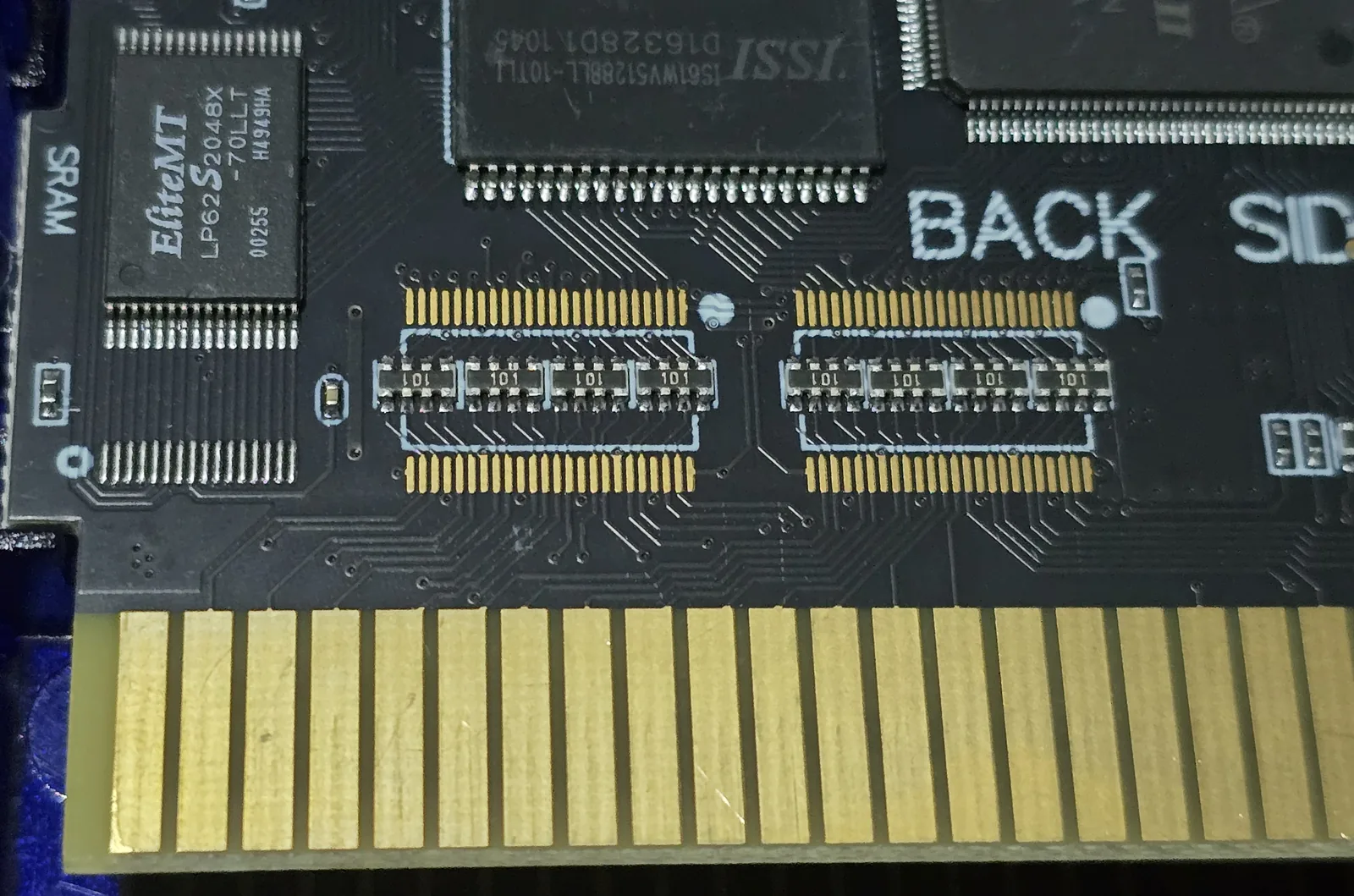
I call this cart acceptable, and worse than a genuine Krikzz, for exactly the reasons above. In normal operation it is inside the Cyclone II’s published clamp rating, so it is not the horror story the “flash carts kill consoles” framing suggests. It also has an unprotected window on every power-on that a buffered cart does not, no isolation of its own switching noise from the console bus, and softer edges. The board was laid out to accept the proper transceivers and shipped without them.
The large QFP on that board reads consistent with an EP2C5T144C8N, the same 144-pin Cyclone II the genuine N8 uses, which is what makes the absent buffers the meaningful difference rather than a wholesale redesign.
The bottom of the spectrum: the cart from my SNES story
This is the other end, and it is the cart that produced the snow and blurry lines described further down this page. I bought it from AliExpress. It arrived dressed as a first-party Nintendo service tool, label and all.
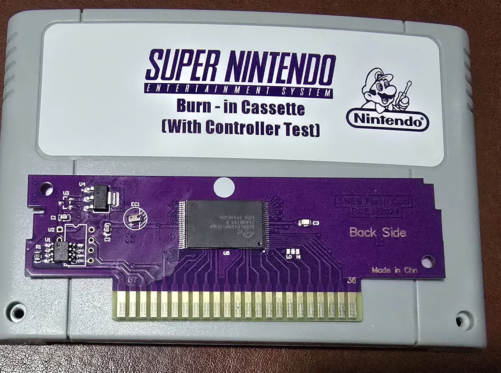
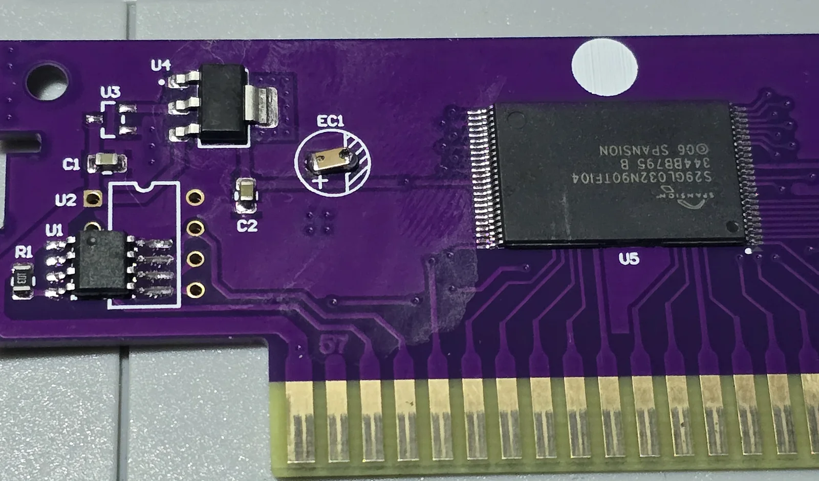
The flash reads S29GL032N90TFI04, a Spansion part. Its datasheet is titled
“S29GL-N MirrorBit Flash Family, S29GL064N, S29GL032N, 32 Megabit, 3.0-Volt
only Page Mode Flash Memory.”
The 04 in the part number decodes, in Spansion’s own ordering table, to
“x8/x16, VCC = 2.7 – 3.6 V, Bottom boot sector.” VIO carries the same
2.7 to 3.6 V range. There is no 5 V-tolerant option anywhere in the family.
That regulator at U4 is the tell that ties it together: the cart takes the console’s 5 V and drops it to roughly 3.3 V to feed the flash. So the chip’s supply rail is 3.3 V while its address and data pins are wired directly to a 5 V bus.
Here is what the datasheet says about that, under Absolute Maximum Ratings:
All other pins (Note 1): –0.5 V to VCC+0.5 V
Note 1: … Maximum DC voltage on input or I/Os is VCC + 0.5 V. During voltage transitions, input or I/O pins may overshoot to VCC + 2.0 V for periods up to 20 ns.
Note 4: Stresses above those listed under Absolute Maximum Ratings may cause permanent damage to the device.
At a 3.3 V rail, the absolute maximum DC voltage on every address and data pin is 3.8 V. The SNES drives 5 V. That is not “outside recommended operating conditions,” which would be the mild version. It is over the absolute maximum, the number past which the manufacturer says permanent damage may result.
The 20 ns overshoot allowance does not rescue it either. It tops out at VCC + 2.0 V and only for 20 ns, while an SNES bus cycle holds an address line stable for somewhere around 280 to 370 ns. The pins sit over the limit for more than ten times the permitted window, on every single cycle, for the life of the cart.
This is the condition the whole page is about, in one photograph: a 3.0-volt-only flash with its own step-down regulator on board, wired straight to a 5 V bus by a manufacturer who fitted neither a buffer nor so much as a resistor. Set against the N8 clone above, the difference is not a matter of degree. That board keeps its FPGA inside a published clamp rating. This one has no protection of any kind.
The cart that fixed it: SNES FlashMaster, and what I got wrong
For years I described the cart that cleaned up my picture as “the one with level shifters.” I finally opened it. It does not have any.
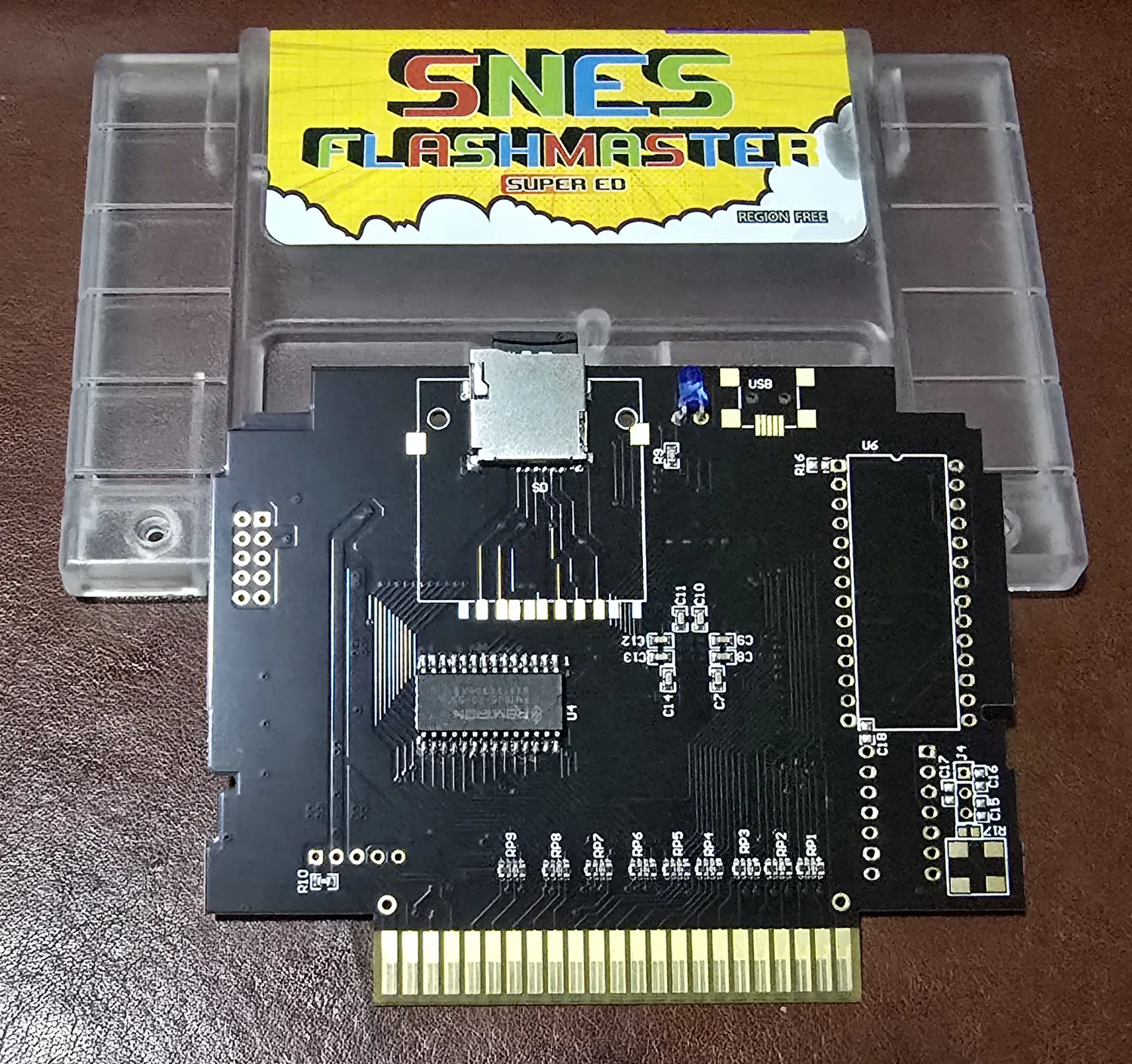
What it actually has is a row of nine resistor networks, RP1 through RP9, all
marked 101, sitting in a line immediately behind the edge connector. Four
elements each, so thirty-six bus lines through 100 Ω series resistance. That is
the same interfacing strategy as the N8 clone, not the transceiver approach I
assumed.
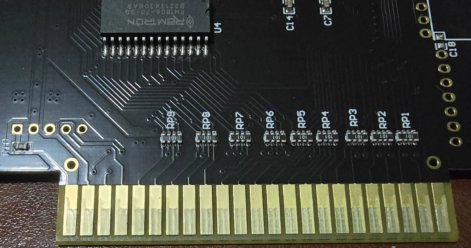
The rest of the board:
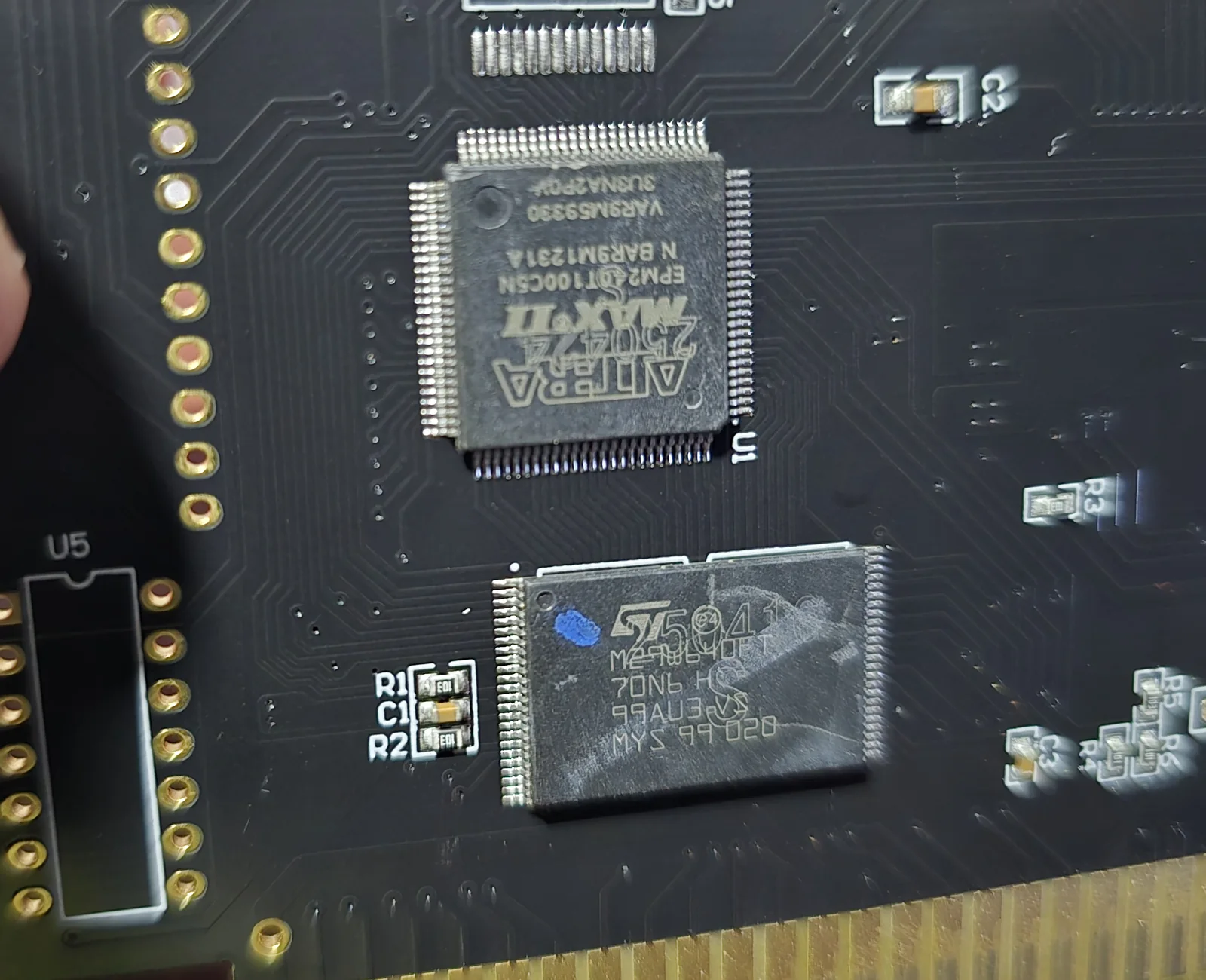
So the two carts are far more alike than my story assumed. Both run a 3-volt-only flash from an on-board 1117-class regulator, on a 5 V bus. The FlashMaster has 100 Ω series resistors on the bus and the burn-in cart has nothing. That, plus the board quality, is the entire difference.
There is a wrinkle here, and it cuts against the FlashMaster. Altera’s MAX II data sheet says, in the notes to its MultiVolt I/O table:
“MAX II devices can be 5.0-V tolerant with the use of an external resistor and the internal PCI clamp diode on the EPM1270 and EPM2210 devices.”
This board uses an EPM240, which is not on that list. The clamp-based 5 V tolerance path that made the N8 clone’s Cyclone II defensible is, by Altera’s own documentation, not offered on this part. And MAX II’s recommended operating conditions cap DC input at 4.0 V, with a duty-cycle table that runs out entirely at 4.5 V and 10%:
| VIN | Max. duty cycle |
|---|---|
| 4.0 V | 100% (DC) |
| 4.2 V | 50% |
| 4.4 V | 17% |
| 4.5 V | 10% |
There is no 5.0 V row at any duty cycle. Which chips actually sit behind RP1 through RP9 I cannot determine from photographs, and the FM1808 being a genuine 5 V part means at least some of the bus needs no protection at all. But the CPLD and the flash both do, and the documented path for protecting the EPM240 the way the Cyclone II is protected does not appear to exist.
So this cart is not the hero of the story I used to tell. It is a better-executed version of the same compromise: series resistance where the burn-in cart has none, roughly eighteen decoupling capacitors where the burn-in cart has four, and a far more carefully laid out board. It is not a buffered design and I should not have described it as one.
The top of the spectrum: SD2SNES, and what “done properly” looks like
Having been wrong twice about what was inside my own carts, I opened the expensive one too. This is an SD2SNES, silkscreened Rev.H2 / 2025, XLLSH. It cost about four times what the FlashMaster did and still about half the price of a genuine Krikzz. I have never had a problem with it, and it runs Star Fox and the other coprocessor titles.
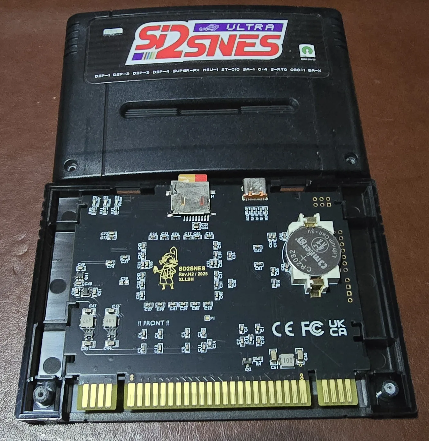
I expected to find the transceivers here, and here they are. U6, U7 and U8 are three 74ALVC164245 parts, 16-bit level-shifting transceivers in 48-pin TSSOP, sitting between the edge connector and the FPGA.
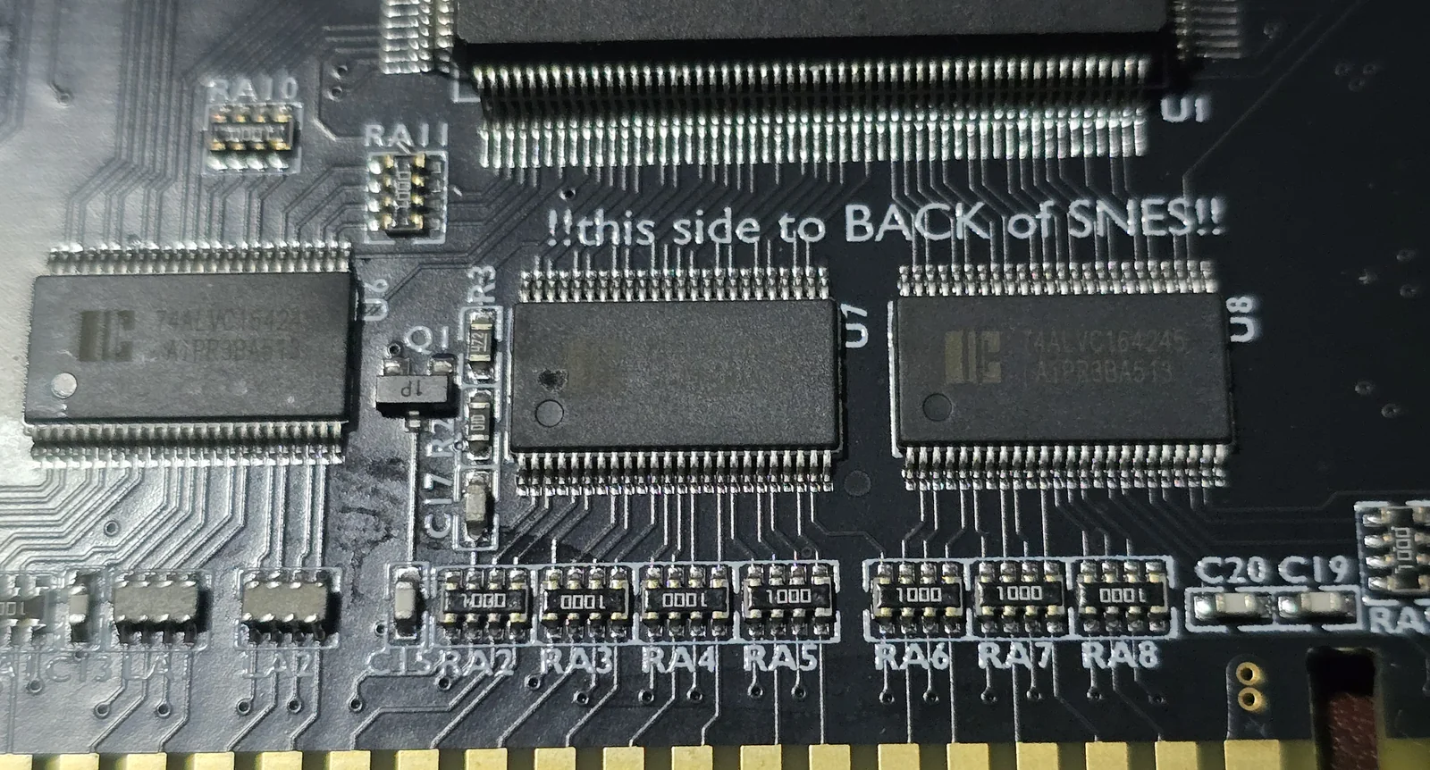
This is the design the sources describe. The community documentation for sd2snes names the 74ALVC164245 specifically (nesdev t=24197, aiju.de), and here it is on the board, three times over.
This is the point the whole page has been circling. Look at what the good board does: it has the 100 Ω resistor arrays and the transceivers. Not one or the other. The genuine EverDrive N8 Pro is the same story, with 100 Ω series resistors on the CPU data lines alongside its buffers. Series resistors are for signal integrity. Transceivers are for level translation and isolation. They are different jobs, and the carts that get it right do both.
Which is exactly why a row of resistor networks tells you nothing on its own. All four of my boards are explained by one question: how far up this list does it go?
| Series resistors | Transceivers | Decoupling | |
|---|---|---|---|
| SD2SNES | RA1-RA11, 100 Ω | Three 74ALVC164245 | Extensive, plus ferrite arrays |
| FlashMaster | RP1-RP9, 100 Ω | None | ~18 caps |
| N8 clone | Eight arrays, 97.2 Ω measured | Footprints present, unpopulated | Moderate |
| Burn-in cart | None | None | Four caps |
Same board, different console: the Mega EverGenesis
Sega gets a turn, and this one is more informative than I expected. This is a “MEGA EVERGENESIS,” the EDMD-family Mega Drive clone.
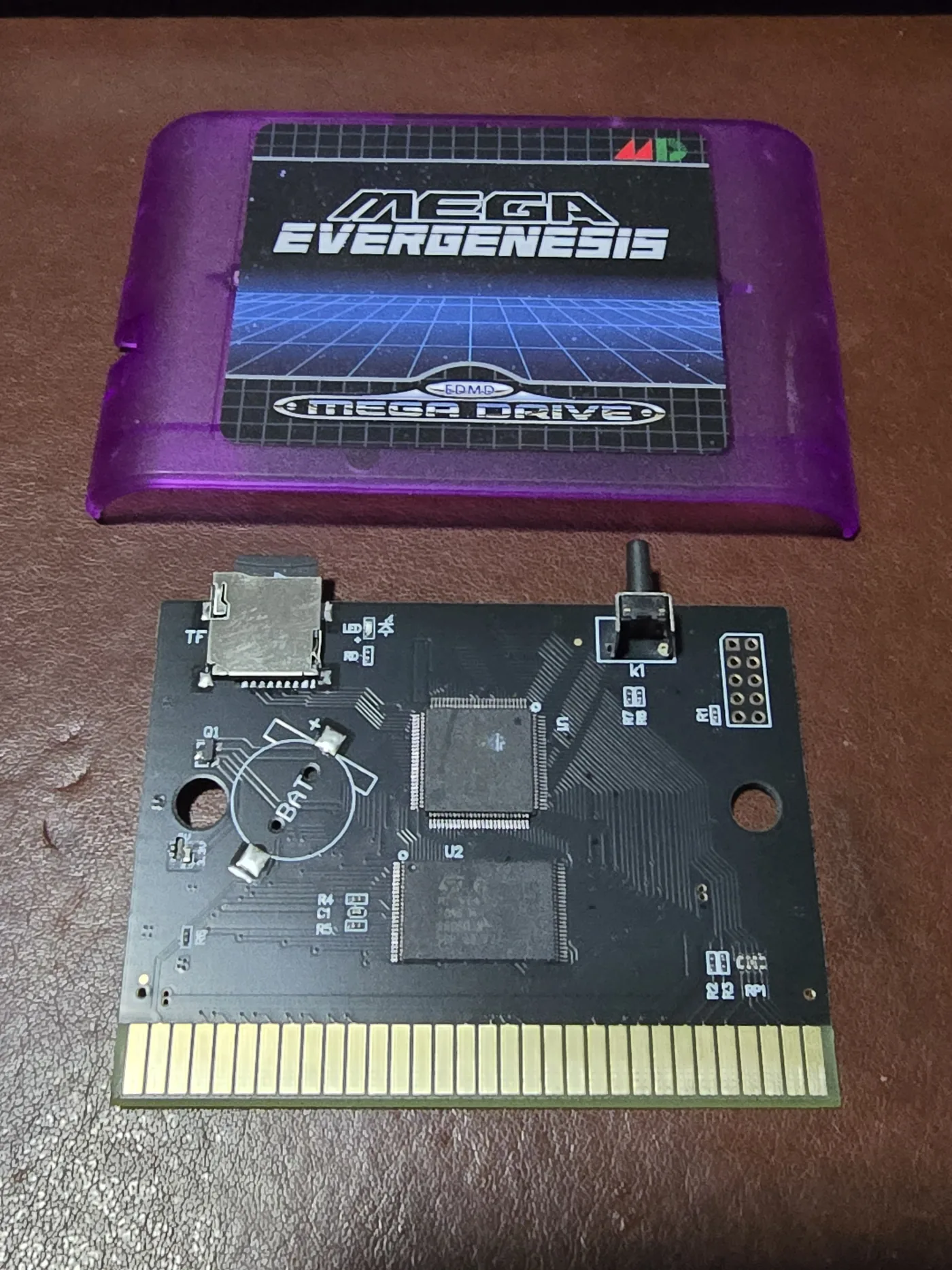
Twelve resistor networks this time, RP1 through RP12, all marked 101. Four
elements each is forty-eight lines, which is about right for a 68000 bus once you
count A1 to A23, D0 to D15 and the control signals. No transceivers anywhere on
the board.
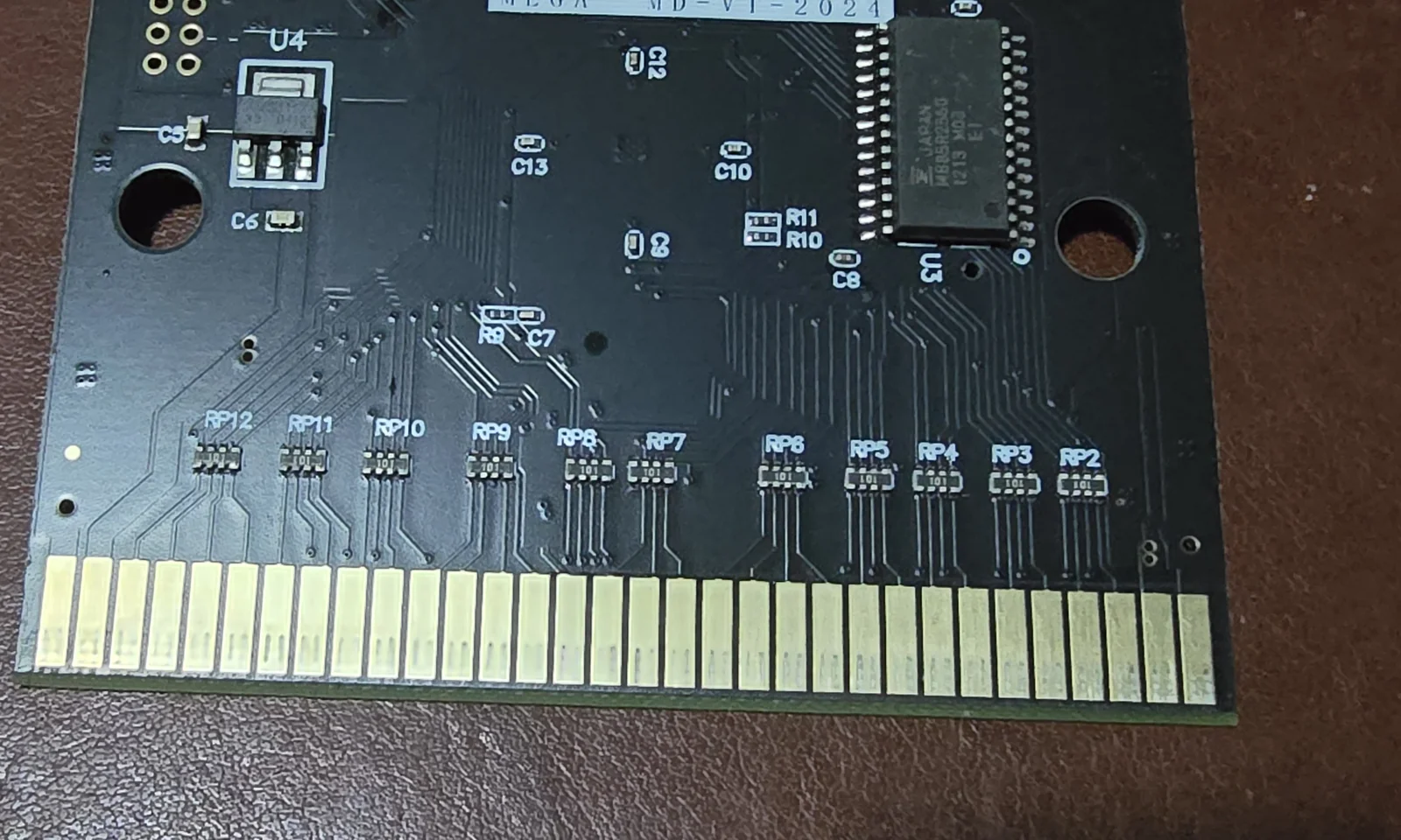
Then I read the two main chips, and the interesting part fell out:
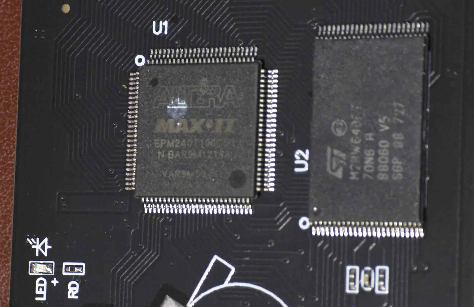
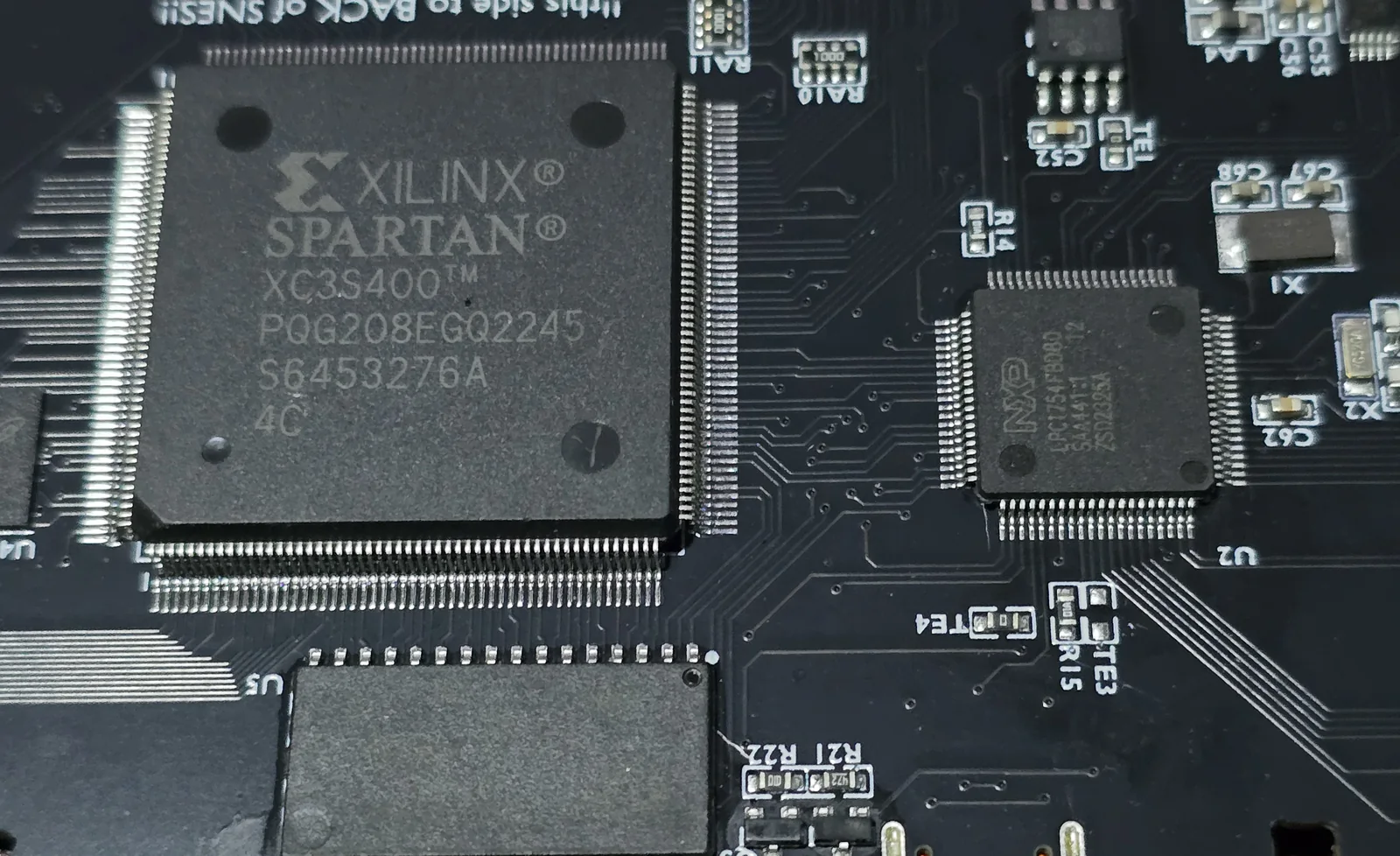
This is the same design as the FlashMaster with a different edge connector. Same CPLD, same flash family, same regulator, same 100 Ω resistor-network strategy, same decision to leave the transceivers out. One design house is shipping one architecture across platforms and reskinning it per console. That tells you more than either board on its own: if you have opened one of these, you have effectively seen the others.
One thing that genuinely differs, and it favors the Genesis: the resistor-only approach is better justified here than on the SNES. Genesis inputs are TTL-threshold and read a 3.3 V high reliably, so the cart-to-console direction needs no translation at all. The SNES is CMOS-threshold and, per nesdev, “requires full translation,” which the FlashMaster does not provide. It works on my bench regardless, which either means the 0.7 × Vcc rule of thumb is conservative or I am running on margin I cannot see. The sources and my bench do not agree here, and I do not know which of them is wrong.
A third console, same recipe: the GB Pro+ (Game Boy)
Game Boy last, and by this point I could guess most of what was inside before the shell came off.
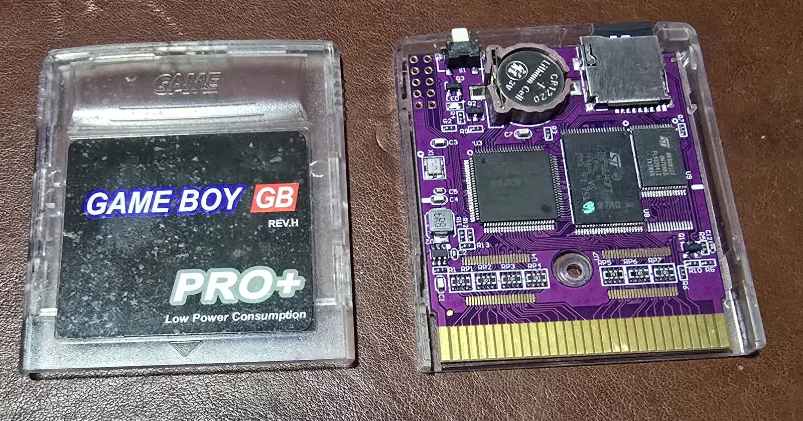
Seven resistor networks along the edge connector, RP1 through RP7. Four to
the left of the shell screw hole and three to the right, and the right-hand three
are legibly marked 101. Seven four-element packs is twenty-eight lines, which
comfortably covers A0 to A15, D0 to D7 and a few control signals.
No transceivers, and this time not even a footprint for one. The N8 clone was laid out for buffers and shipped without them. This board was never laid out for them at all, which puts it a step further down than the N8 clone rather than alongside it.

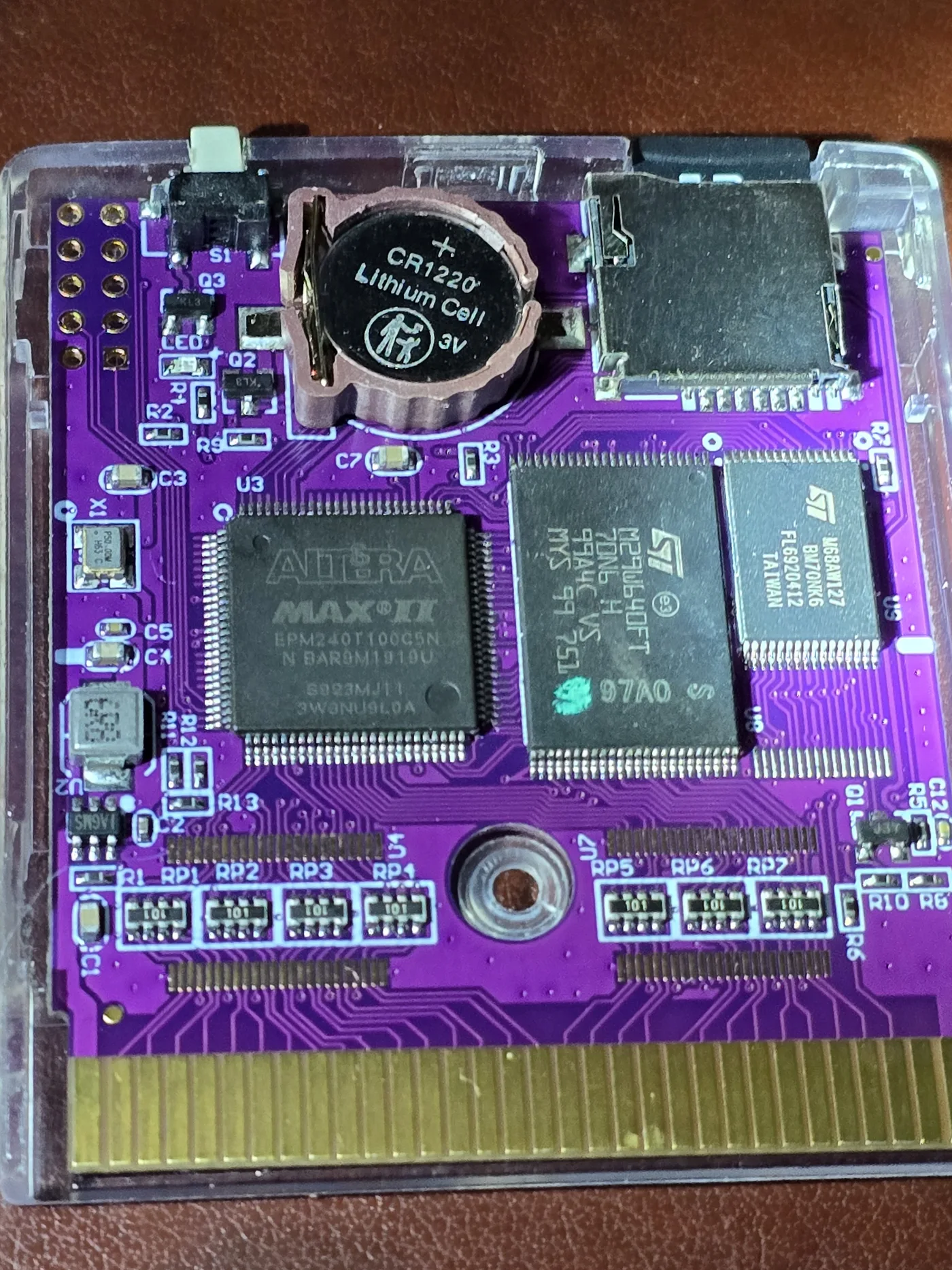
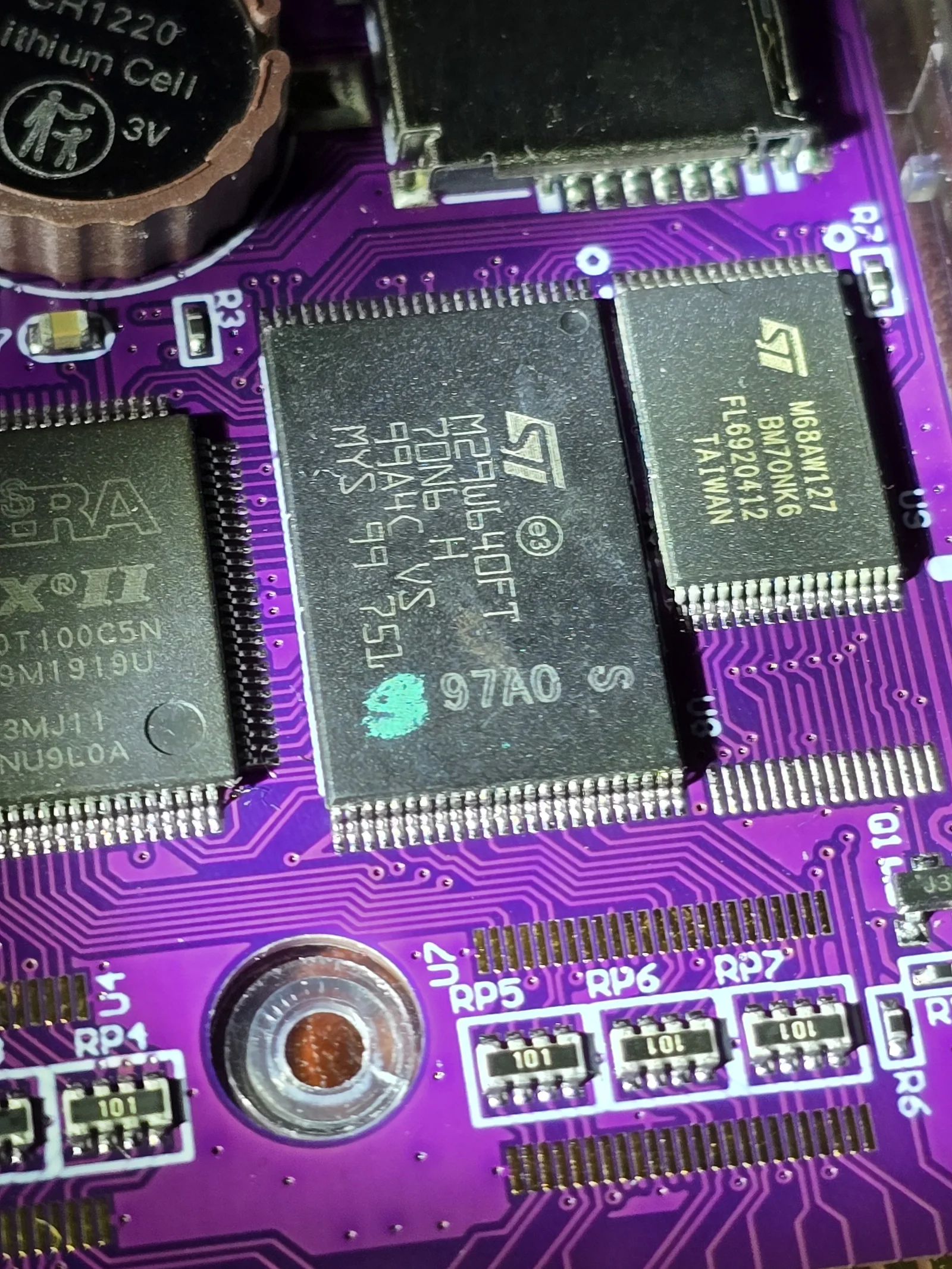
Then I read the three main chips, and there is nothing left to hedge:
- U3 is an Altera MAX II
EPM240T100C5N. The same CPLD, down to the ordering code, as the SNES FlashMaster and the Mega EverGenesis. - U8 is an ST
M29W640FT, a 64 Mbit (8 MB) 70 ns NOR flash. Again the same part as the other two boards. This holds the ROM. - U9 is an ST
M68AW127, a 1 Mbit (128K x8) 70 ns asynchronous SRAM. This is the RAM, and it is what the coin cell is keeping alive.
Add the 101 networks at the edge connector, no transceivers, and the same empty
2x5 programming-header footprint the FlashMaster leaves bare at J3, and this board
is the FlashMaster recipe part for part.
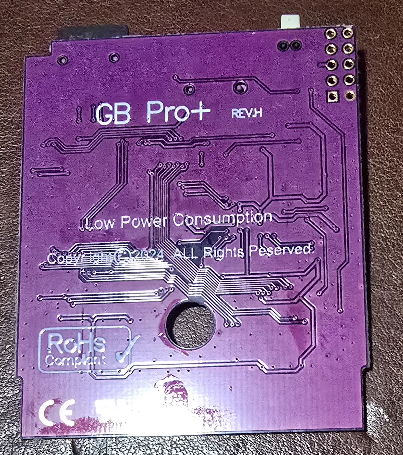
So the “one design house, one architecture, reskinned per console” pattern runs to three platforms, and this third one is an 8-bit handheld rather than another 16-bit console. Same CPLD ordering code, same flash part number, same 100 Ω strategy, same decision to leave the transceivers out, on the Game Boy bus as on the SNES and the Mega Drive. Open one of these and you have genuinely seen the others.
Worth pinning down what those two memory parts are rated for: the M29W640FT and
the M68AW127 are both 3.0 V devices, 2.7 to 3.6 V, and both sit on the Game
Boy’s 5 V bus behind nothing but the 101 networks. The exposure this page
describes for the CPLD is not the CPLD’s alone.
The Game Boy is also the console where resistors-only has the least going for it. Game Boy inputs are CMOS-threshold, the same as the SNES, so this board lands in the strict row of the table near the top of this page and not the forgiving Genesis one. It works on my bench regardless. That makes two boards here sitting on the wrong side of the same rule of thumb and running fine, which is either a conservative rule or margin I cannot see, and I still cannot tell which.
One practical note, since I had this one open to service it. Its CR1220
arrived flat, 0.0 V on the meter, and the symptom was that the cart forgot its
settings: which ROM was loaded, cheat codes, that kind of state. The cell sits in
a clip rather than soldered down, so it changes with a screwdriver and no iron,
which is the opposite of the tabbed cells in the battery-backed game cartridges
covered elsewhere on this site.
Reading U9 makes the rest of that story fairly clear without my having tested it.
128K x 8 is exactly the largest save RAM a Game Boy MBC5 cartridge can carry, so
that SRAM is almost certainly standing in for cartridge save RAM rather than being
scratch space for the menu, and the cell is holding both. The distinction is worth
keeping because the only thing I actually watched fail was the settings.
The reputation map, including the part people get wrong about the good brands
The trusted names are Krikzz (the EverDrive line), the community sd2snes/FXPAK, and Terraonion. Their current-generation models use proper translation. Their N64 and GBA carts are safe by construction, since there is no mismatch to get wrong on a 3.3 V bus.
The nuance most people miss is that this was not always true, and it is Krikzz’s own older 5 V-console models that are the exception. Nerdly Pleasures' teardown survey lists Mega EverDrive v1, v2 and X7, FlashKit MD, EverDrive MD v1 to v3, Master EverDrive, Turbo EverDrive v1, Super EverDrive v1 and v2, and EverDrive GG as using only current-limiting resistors or too few translators. Krikzz responded publicly and redesigned, and the same source calls the EverDrive N8, all EverDrive GB models, Mega EverDrive X3 and X5, and Turbo EverDrive v2 quality products that “use an appropriate number of logic level translators.”
I treat that with medium confidence, for two reasons. The board-level specifics rest largely on that single respected teardown, which the manufacturer acknowledged; Krikzz disputed the “dangerous” severity framing rather than the board descriptions. And I have never owned an EverDrive of any generation, so I cannot put a meter on one, which is how I check everything else on this site. The practical takeaway is stable either way: a genuine current-generation cart is the safe pick, and a very old EverDrive is worth checking rather than assuming.
Since first writing that, a reader sent me photographs of six genuine Krikzz boards, which is not a meter but is a great deal better than trusting one teardown. They confirm the Master EverDrive and the Mega EverDrive X3 and X5 entries above, and they show that the “Super EverDrive v1 and v2” entry needs a revision boundary rather than a version range. The boards are further down this page.
Clones of genuine flash carts carry two separate problems. Level shifting is unknown per unit, since nobody publishes their schematics and the build varies. And genuine EverDrive firmware contains DRM that deliberately bricks clones, so a clone that takes an official firmware update can be permanently flash-wiped and recoverable only over JTAG (Emulation General Wiki). That second one has nothing to do with electricity and takes out more clones than voltage does. I sell tested clone carts and say so plainly on each listing, including what they are not.
Pirate multicarts and bootleg repros are where skipped shifting is most likely, because the boards are built to a price with no programmable logic at all. A concrete documented example: the Genesis bootleg Leaded Solder tore down runs a salvaged 3.3 V Toshiba flash on the 5 V bus “without any level shifting, buffering, or even a voltage-dropping resistor.” That is one author’s inspection of one cartridge, and I record it as exactly that rather than as proof that all bootlegs do this.
Where the public evidence is genuinely thin: verified teardowns of specific AliExpress N8 and EDMD clones, and of the pirate “150-in-1” style multicarts, are scarce. I will not assert that a given clone has no level shifter without opening it or pointing at a real teardown, and neither should anyone else.
Six genuine Krikzz boards, sent in by a reader
Twice above I asked whether anyone who owns a genuine EverDrive would photograph the strip of board between the edge connector and the chips. Someone did. Reddit user Boomerang_Lizard read this page and sent me 108 photographs of seven cartridges covering five consoles, six of them genuine Krikzz. Every photograph in this section is his.
Two limits before the boards. These are still not bench evidence: I have not measured any of them, and a meter does not fit through a photograph. Every part number below is read off the chip markings in his images. And the boards are the ones he happens to own, which is not a survey.
With that said, this is the first primary evidence this page has had for the hardware its whole comparison is measured against, and it lands on both sides.
Master EverDrive: what resistors-only looks like on a genuine board
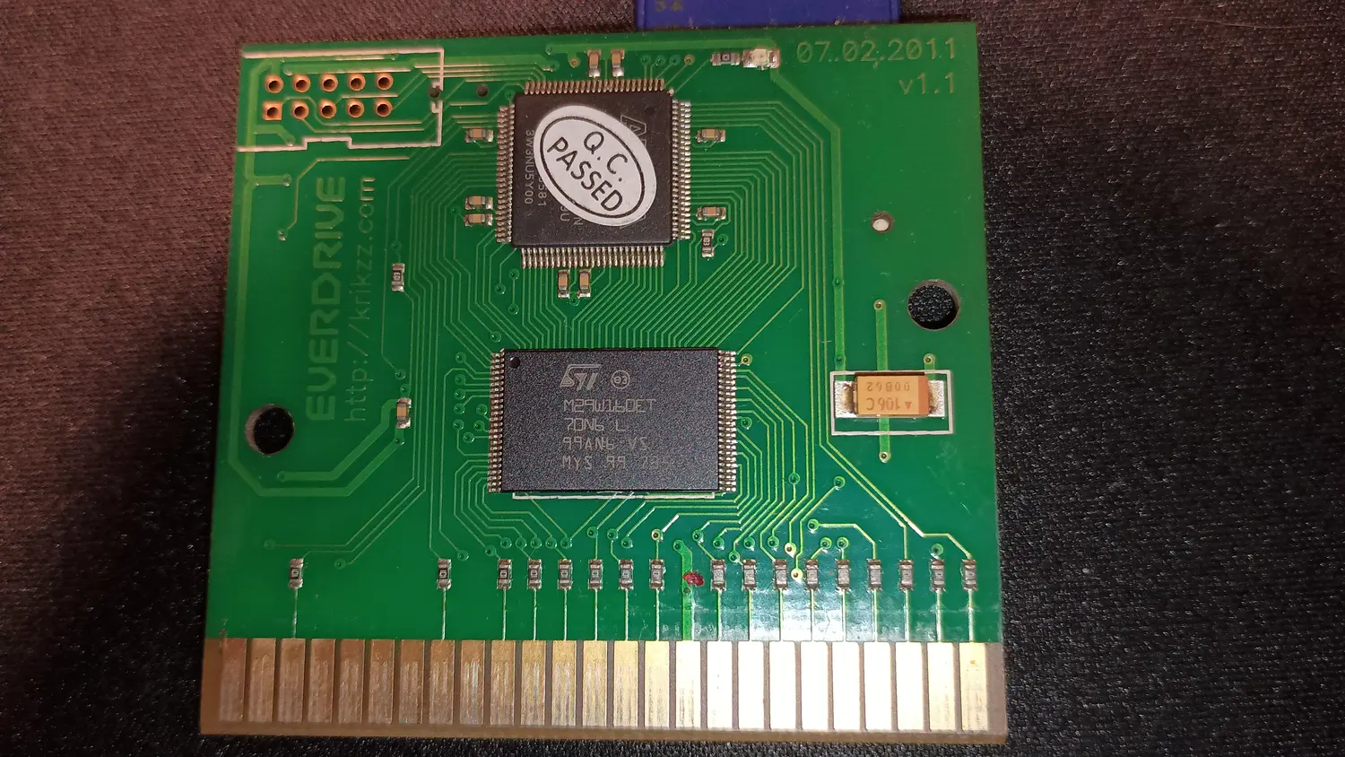
Master EverDrive is on Nerdly Pleasures’ resistor-only list, and that list was the single source I flagged as medium confidence a few paragraphs ago. Here is an independent photograph, from a different owner, showing exactly what the list claims. Compare it with the N8 clone at the top of this page: the clone fits resistor networks into empty buffer footprints, while this board was never laid out for buffers at all.
After the redesign: Mega EverDrive X3 and X5
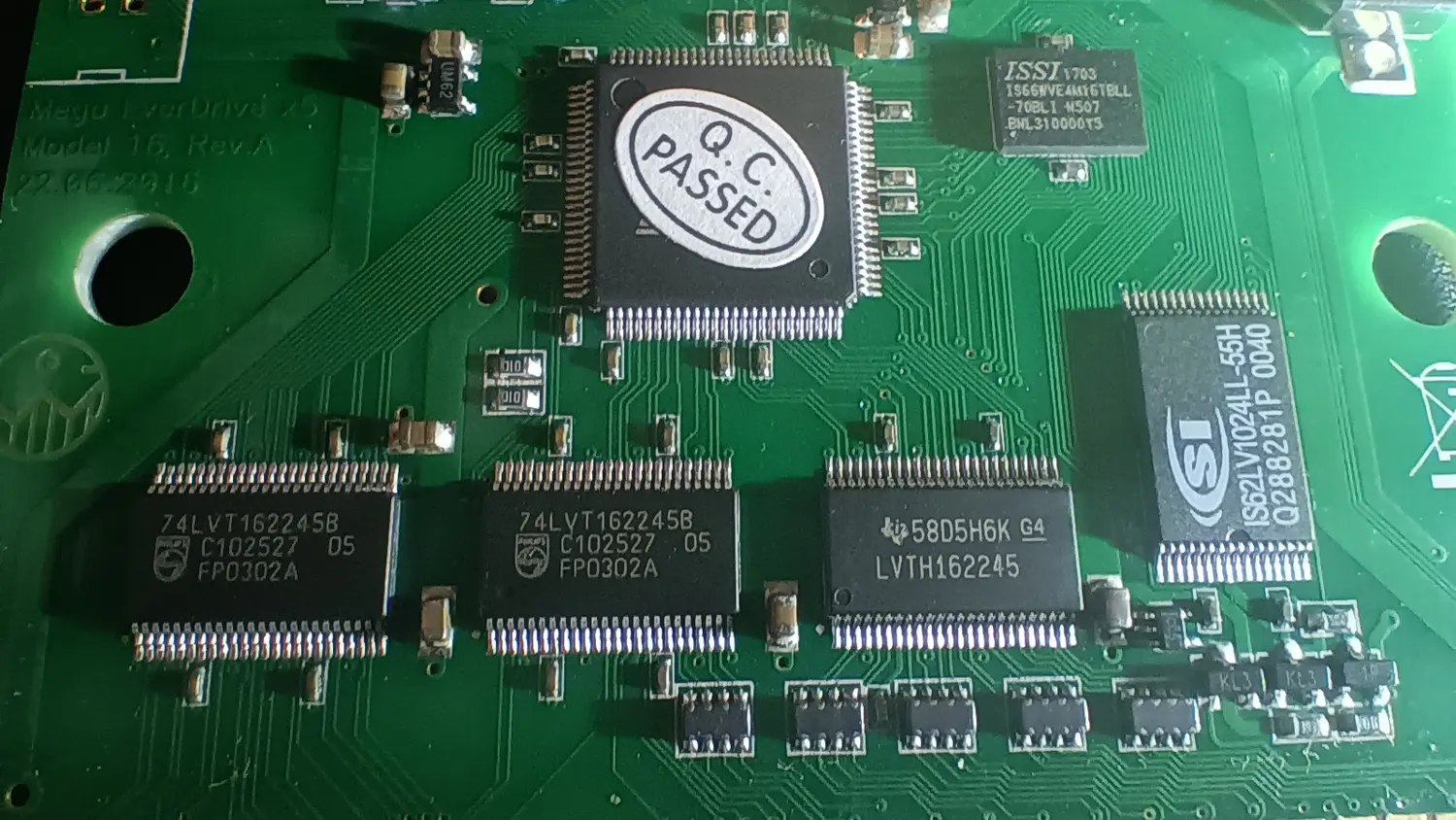
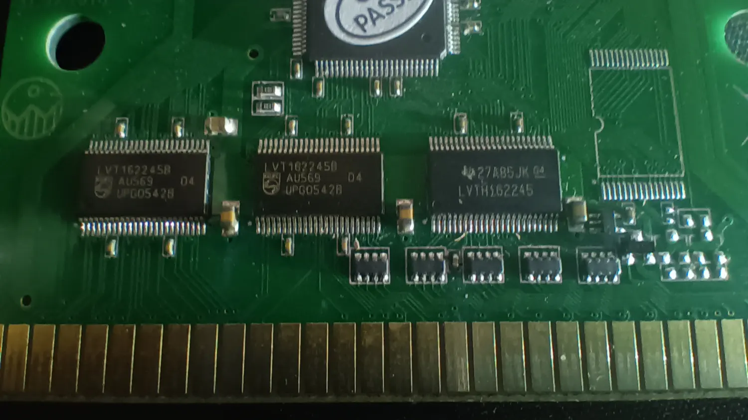
Both of these are on the list of models Krikzz redesigned, and both have the translators the list credits them with. That part of the reputation map holds up.
Super EverDrive v2.3D: the version range needs a boundary
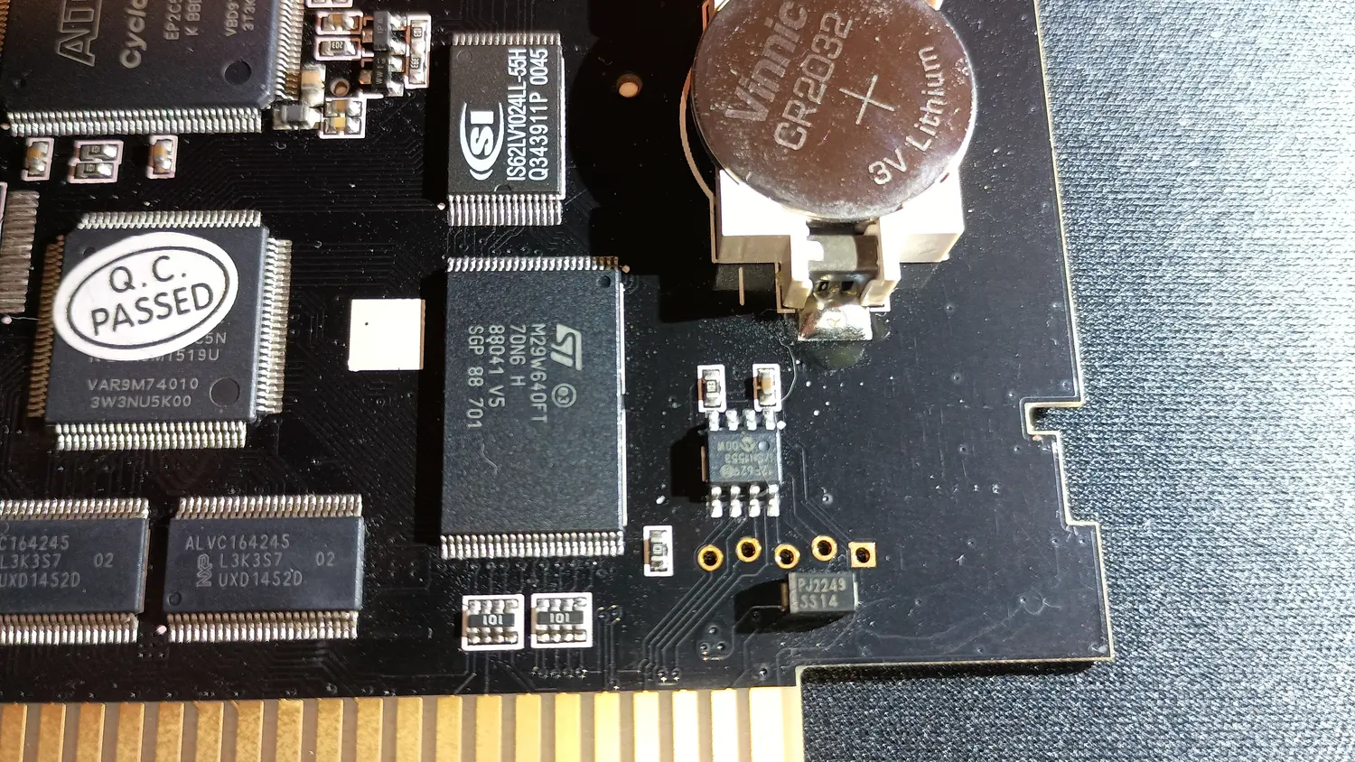
This one complicates the reputation map rather than confirming it. Nerdly Pleasures lists “Super EverDrive v1 and v2” as resistor-only, and this board is a v2.3 carrying proper translators. The date decides it for me: December 2014 is well after Krikzz responded publicly and redesigned, so the sensible reading is that the range stops short of the 2.3 respin rather than that the survey is wrong. Either way, do not repeat that list as a version span. Name the revision, because the revision is what determines the answer.
EverDrive N8: the part is not the one the wiki names
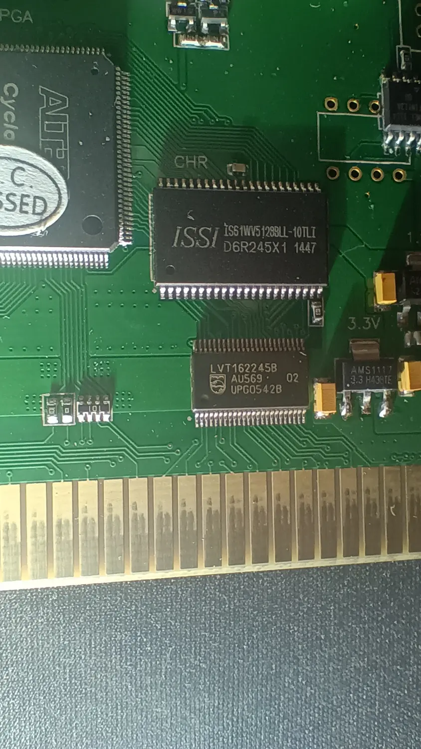
That is worth knowing if you are ever identifying a board by its buffer part number: you cannot. Both parts are legitimate 16-bit translators, and a manufacturer substitutes across a production run for reasons that have nothing to do with you. What matters is whether the buffers are there, not which ones.
EverDrive 64: nothing to shift
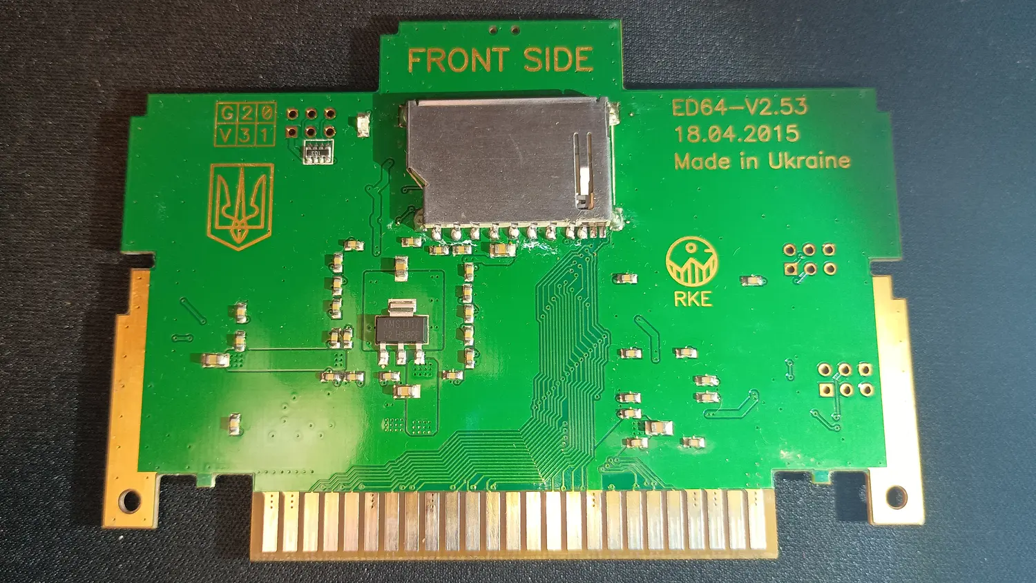
The seventh board is a clone, and it does the job anyway
He sent this one as an SD2SNES Rev-X. It is not one.
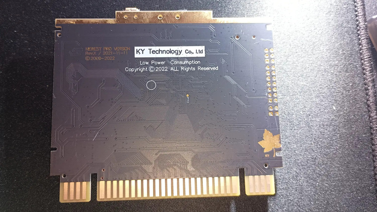
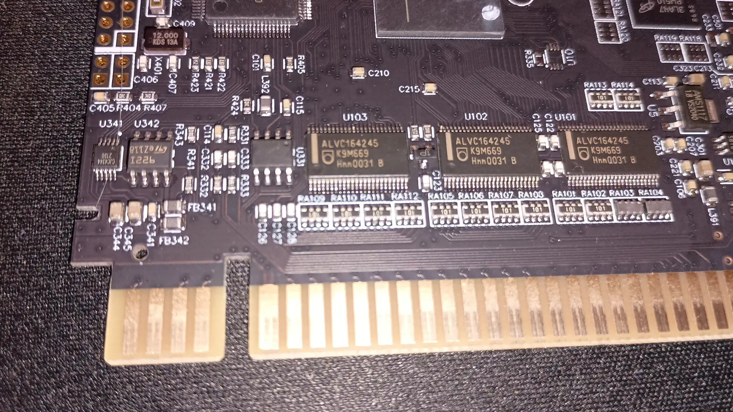
I find this the most useful board in the set, because it argues against a shortcut I have been close to taking myself. “Clone” does not mean “unshifted.” This one copied the reference design faithfully on the thing that actually matters electrically. The real risks of buying a clone are the firmware DRM above, build and test quality, and having nobody to go back to when it fails. Those are good enough reasons to buy genuine. The bus is not automatically one of them.
None of this touches the gap I flagged earlier. These are Krikzz boards and one KY Technology clone of an open design. The AliExpress N8 and EDMD clones, and the “150-in-1” multicarts, are still undocumented, and one well-built clone says nothing about them.
If you own something in this space and are willing to photograph the strip of board above the edge connector, the offer stands. It is how this section exists.
The picture-quality question, where I was wrong first
A cartridge is a digital device and it is not in the console’s analog video path. That is the console’s PPU DAC and encoder doing that work. So a cartridge cannot improve your picture. Anything selling you a “sharper” or “cleaner” image from a cartridge is audiophile-grade nonsense.
I originally took that one step further and wrote that a cart therefore cannot affect analog video at all. That was too strong, and my own bench proved it to me. The reverse is real: a noisy cartridge can degrade the picture, by injecting digital switching noise into the 5 V rail and ground return that the console’s video circuitry is also using. It is not in the signal path. It is a dirty neighbor on the same power.
This is documented on the NES, where flash carts produce visible jailbars in composite output and it varies by cartridge model on the same console: the PowerPak is the noisiest, the EverDrive N8 much less so, and genuine cartridges show little to none (Nerdly Pleasures, nesdev t=13219). Same console, different cart, different noise, which is direct proof that a cartridge can reach the picture. The mechanism for the NES case is “capacitive or power rail coupling between PPU A13 and the video signal” (nesdev t=16607).
Cartridge decoupling exists specifically to fight this. Mousebite Labs’ writeup on SNES cartridge design says carts should carry decoupling capacitors “to filter out any stray noisy signals that may be propagating through the VCC line,” a 22 µF electrolytic plus a 0.1 µF ceramic per major chip, and nesdev t=9623 documents instability fixed by adding 100 nF per chip. A bootleg that skips that is electrically louder than one that does not.
There is also a real counter-example: one SNES owner found no video-noise difference at all between an SD2SNES and original carts (shmups t=65781), and some SNES speckle originates in the console’s own board revision rather than anything you plugged into it. Both of those are consistent with the physics. An SD2SNES already has buffers and proper decoupling, so it was never going to be the noisy offender. A bootleg with no bus interfacing at all is a different animal.
My bench: a bare-bus SNES cart put snow on three consoles
Here is where I ran into this. I could not find it documented anywhere, and I went looking. The canonical SNES level-shifting threads (nesdev t=257404, t=9907) discuss buffering purely as a damage and reliability matter and never mention video, noise or coupling at all. So take this as my own observation rather than something you can go read a second source on.
I had a cheap Chinese SNES burn cart, the one torn down above: a 3.0-volt-only Spansion flash on its own step-down regulator, wired directly to the 5 V bus with no buffer and no series resistors anywhere on the board. The picture was poor: snow in places, and blurry lines. I blamed the consoles. I went through three SNES units in a row suspecting each of them of bad video output.
Before I found the cause I tried the obvious things and none of them helped. I put a large filter capacitor across the 5 V rail. I verified the PSU was delivering good clean power. I tried several other fixes. No change.
Then I ran the same ROM from my SNES FlashMaster. The video was about a hundred times better, on all three consoles.
Same ROM, three consoles, only the cartridge changed. That puts it well past anecdote: three in a row rules out one flaky console, and the cart is the variable. The failed bulk capacitor is diagnostically useful too, because it matches the sourced physics. Bulk electrolytics do nothing for the high-frequency local coupling that causes this, which is also why the claim that replacing electrolytic decoupling caps fixes NES jailbars does not hold up (nesdev t=16607). What helps is a clean, well locally decoupled cartridge, not a big cap across the rail.
What I got wrong about this for years, and the correction matters. I used to tell this story as “unbuffered cart bad, buffered cart good.” Then I opened both carts to photograph them for this page, and the FlashMaster turned out to have no buffers or transceivers at all: just nine 100 Ω resistor networks at the edge connector. Both carts run a 3-volt-only flash off a 1117-class regulator on a 5 V bus. So this was never a test of buffering.
What it was a test of, once you line the two boards up:
- Series resistance on the bus. Thirty-six lines through 100 Ω on the FlashMaster, versus a direct connection on the burn-in cart. Series resistors damp ringing and slow edge rates, which is exactly the kind of thing that reduces coupled noise.
- Decoupling. Roughly eighteen capacitors on the FlashMaster against four on the burn-in cart, and the FlashMaster’s are clustered right at the chips where they do something.
- Board quality. Layout, ground pour and routing discipline, which I cannot quantify from the outside but which are visibly not comparable.
So the defensible conclusion is narrower and more useful than the one I used to draw: a competently interfaced and decoupled cartridge gave a clean picture where one with no bus interfacing at all gave snow. Buffering was never the variable, because neither cart had any. Anyone repeating “buffered carts give cleaner video” on the strength of my story, including me, was overreaching.
The airtight version of this test remains two otherwise identical carts differing in exactly one thing, and I still have not built it.
The bench lesson is the useful part, and it is on my SNES reference too: before you condemn an SNES’s video, swap in a known-good genuine cartridge. I nearly wrote off three working consoles.
Black screen and reset loop is lockout, not damage
This one gets misread constantly, so it is worth separating out. On the NES and SNES a lockout CIC has to complete a handshake before the console comes out of reset. On the SNES the lock CIC drives separate reset lines to the cartridge CIC and to the console (SNESdev). When the handshake fails, because of a wrong region key, a missing CIC, or a clone that cannot authenticate, “the lock will pull the /CPU & PPU RESET line low with a 1Hz square wave” (nesdev). That is the classic flashing black screen at about one hertz. ConsoleMods describes the same thing: a mismatch “will hold the system in a reset state” (consolemods.org).
Nothing is being damaged while that happens. It is an authentication failure and it stops as soon as you remove the cartridge.
Historically some unlicensed publishers defeated the CIC by generating out-of-spec negative voltage waveforms to freeze the lock chip, which nesdev attributes to Camerica, Color Dreams, AVE and AGCI. That technique worked, and it is also a fair reason people are wary of what unlicensed boards put on the bus.
The thickness question: a real mechanism I could not find in the wild
Everything above is about electricity, and the electrical console-damage claims did not survive checking. There is a second claim, mechanical rather than electrical, that people raise about repros and clones: the board is thicker than an original, and it spreads or bends the pins in your console’s cartridge slot.
That one holds up, with an important restriction most people leave out.
Why it happens
A card-edge connector is a row of spring contacts sized for a specific card thickness. Push a thicker card in and you deflect those springs further than they were designed for. Do it enough and they take a permanent set, which means less contact force on every cartridge you insert afterwards, original ones included. The classic symptom is the connector that will no longer read anything reliably.
The reason repros hit this so often is boring: 1.6 mm is the default thickness at essentially every PCB fab. Order a board without specifying, and 1.6 mm is what arrives. Whether that is a problem depends entirely on which console you are building for.
The correct thickness is not the same across consoles
This is the part that gets flattened into “repro boards are too thick,” which is wrong about half the time:
| Platform | Correct board thickness | Fab default of 1.6 mm is |
|---|---|---|
| NES / Famicom | 1.2 mm ±0.05 | 33% over |
| SNES / Super Famicom | 1.2 mm | 33% over |
| Genesis / Mega Drive | 1.6 mm | correct |
| Game Boy / GBC | 0.8 mm | double |
The NES figure is from the NESdev wiki’s cartridge dimensions page, which lists board thickness as 1.2 mm ±0.05 mm from vernier-caliper measurements. For the SNES, qwertymodo on nesdev: “the proper thickness is 1.2mm (I just measured one to confirm)” (t=9236). The Mega Drive figure comes from the smdCart cartridge project, which states plainly that “MegaDrive carts have thickness of 1.6mm,” and the Game Boy figure from the DMG-DECN-02 board recreation, which specifies 0.8 mm.
So a Genesis repro built on the fab default is dimensionally correct and this whole concern does not apply to it. A Game Boy repro on the default is twice the thickness it should be, which is the worst case in the table by a wide margin.
How much thickness is too much
The most useful numbers come from Memblers on nesdev, who has actually manufactured cartridge boards in quantity (t=7663):
“When I measured Nintendo’s boards before it came out to be 45 mils.”
“60 mils will ruin the NES connector. It’s especially bad for top-loaders.”
“all the boards I’ve made are 47 mils, and I’ve never heard any complaints (Squeedo rev2 was used in hundreds of MidiNES cartridges).”
In millimetres that is 1.14 mm original, 1.19 mm proven harmless across hundreds of units, and 1.52 mm as the point where he says the connector is ruined. The fab default of 1.6 mm is 63 mils, past that line. In the same thread lidnariq measured a Nintendo board at around 52 mils, with traces adding roughly 2 mils per side, so treat the original figure as somewhere in the 45 to 52 mil band rather than a single number.
Memblers grounds the damage claim in something most people have seen: “You only have to use a Game Genie a lot to find that out.” The Game Genie’s board is notoriously thick, and spread NES connectors are a well-known consequence of heavy use.
Where the evidence is thinner: the SNES version of the claim is an inference, not a measurement. The nesdev poster’s exact words are “I figure a 1.6mm would damage the snes cardedge connector,” which is reasonable engineering judgement given the 1.2 mm spec, but nobody in that thread measured a spread SNES connector. So take the NES claim as practitioner experience and the SNES claim as extrapolation from a known-correct spec.
So I measured mine, against genuine cartridges
Published numbers are one thing. Here is what a caliper says about nine cartridges on my bench, five aftermarket and four genuine, all measured the same way in one sitting.
That last part matters more than it sounds. Comparing my carts to a published figure would leave the door open to a systematic offset in my tooling or technique making everything read high or low. Comparing them to genuine cartridges measured on the same calipers in the same session closes it, because whatever offset exists applies equally to both. The relative comparison is the one worth trusting, and it is the one that answers the question.
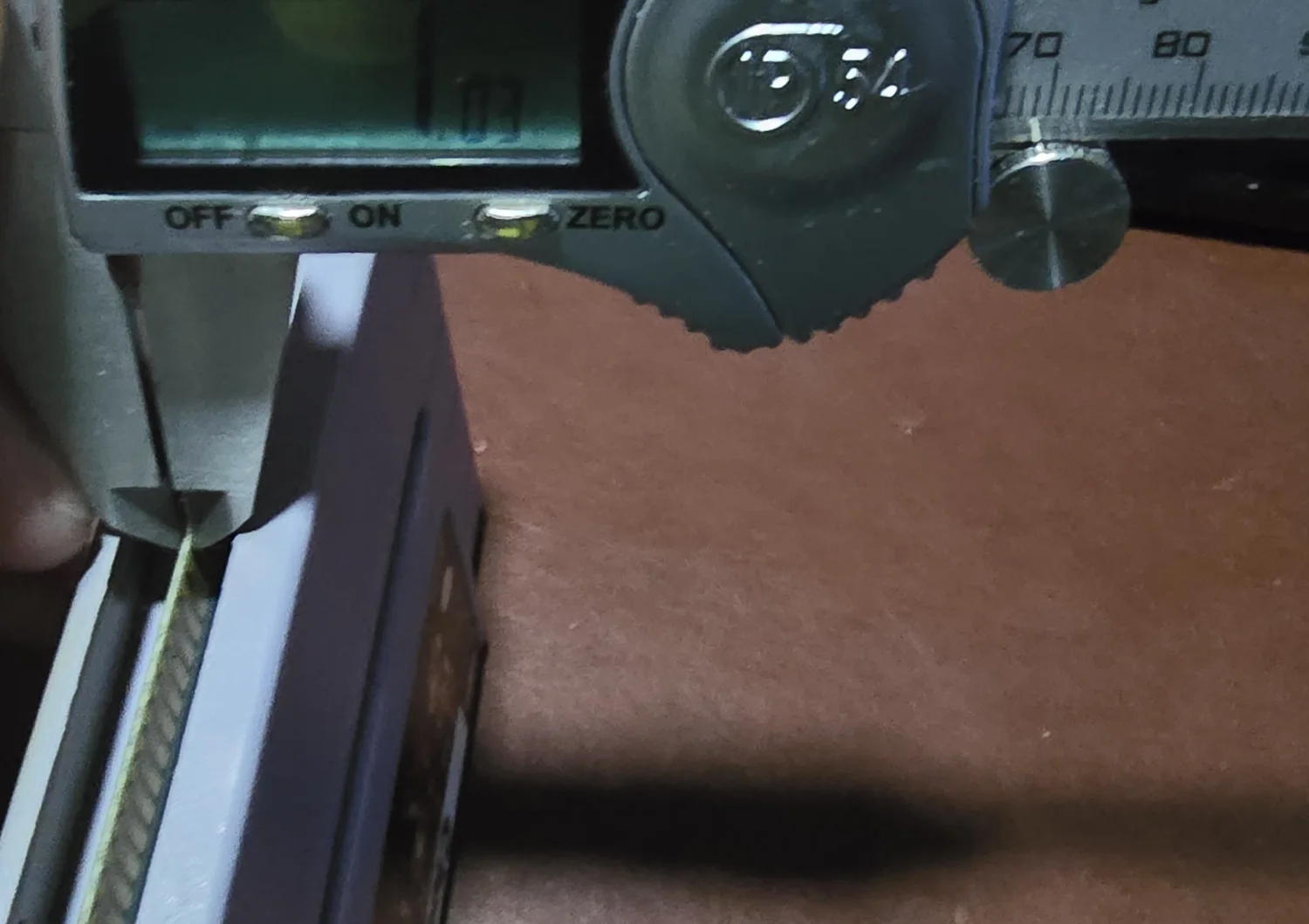
| Cartridge | Genuine? | Thickness at the contacts |
|---|---|---|
| Dr. Mario, NES | Genuine | 1.08 to 1.12 mm |
| Clue, SNES | Genuine | 1.03 to 1.16 mm |
| Super Game Boy, SNES | Genuine | 1.04 to 1.12 mm |
| Genesis cartridge | Genuine | 1.50 to 1.55 mm |
| SNES burn-in bootleg | Bootleg | 1.03 mm |
| SD2SNES | Third-party build | 1.01 to 1.05 mm |
| EverDrive N8 clone, NES | Clone | 1.10 to 1.18 mm |
| SNES FlashMaster | Clone | 1.20 mm |
| Mega EverGenesis, Genesis | Clone | 1.45 to 1.50 mm |
Not one of the aftermarket carts is meaningfully thicker than my genuine ones. The thickest of the five, the FlashMaster at 1.20 mm, sits 0.04 mm above the highest reading I got off a real Nintendo cartridge, which is inside the scatter of the measurement rather than a hazard. Two of them, the bootleg and the SD2SNES, are at or slightly below the thinnest genuine cart I measured.
The Genesis pair is the cleanest comparison of the lot, because there I have a clone and a genuine cartridge for the same platform: the Mega EverGenesis measures 1.45 to 1.50 mm and the real Sega cartridge 1.50 to 1.55 mm. The clone is marginally thinner than the original it copies, which is the direction every other comparison on this page points too.
For scale: Memblers’ figure for the thickness that ruins an NES connector is 60 mils, which is 1.52 mm. Nothing I own for NES or SNES is within a third of a millimetre of it.
Two further observations from the bench:
- Plating is a real part of the number. On the bare board between the contacts I read 1.00 to 1.05 mm; across the contacts themselves, 1.08 to 1.18 mm. That is roughly 0.05 mm per side of copper and gold, which matches lidnariq’s estimate on nesdev of about 2 mils per side almost exactly. If you are checking a cart yourself, measure across the contacts, because that is what the connector actually grips.
- Nobody bevels these, including Nintendo. I looked for a lead-in chamfer on all nine and found at most a very subtle rounding, with the genuine cartridges no better than the clones and in some cases slightly less rounded. So the absence of a crisp bevel on a repro is not the tell it is sometimes described as. The NESdev dimensions page does not specify a chamfer either.
One wrinkle in the absolute numbers: every genuine cartridge I measured came in below its platform’s published thickness. The Nintendo carts read under the 1.2 mm ±0.05 on the NESdev wiki even across the contacts, and the Sega cartridge read 1.50 to 1.55 mm against a 1.6 mm figure. Whatever is going on, it is going on consistently, in the same direction, on both platforms.
Some of that spread is already in the sources: Memblers measured Nintendo boards at 45 mils (1.14 mm) and lidnariq at around 52 mils (1.32 mm), for what should be the same object. My reading is that Nintendo built on 1.0 mm stock and finished near 1.1 mm at the contacts, and that the published figures sit at the upper end of a genuinely variable population. It is also possible my calipers or my technique run a hair low. I cannot separate those two possibilities from here.
But it does not matter for the question this measurement was asked to answer. Every cart, genuine and aftermarket, went through the same calipers in the same session, so any offset applies to all of them equally. The relative result stands regardless of where the absolute numbers land, and the relative result is that my clones are not thicker than my originals.
What this means in practice
The mechanism is real, but I could not find it in the wild. Nine cartridges, four platforms, and not one aftermarket board was thicker than a genuine one. If you are going to worry about a cheap cart, the electrical side of this page deserves the worry far more than the mechanical side does.
The consoles where it could bite are NES, SNES and Game Boy, because their specs sit under the 1.6 mm every PCB fab defaults to. On a Genesis the default is the spec, so the concern evaporates.
Game Boy and Game Gear look like the worst case on paper and are actually the safest, because on those two the board is not what the connector grips. Pull a Game Boy or Game Gear cartridge and look at the bottom edge: contacts on one face only, and the other face is not exposed at all. It is shell plastic. What slides into the console is a tongue made of PCB on one side and moulded shell wall on the other, and the console’s slot is sized for that laminate rather than for a bare board.
That makes the shell the gate, twice over. A 1.6 mm board has to seat in a channel moulded for a 0.8 mm one, and then the resulting thicker tongue has to enter a slot that was never sized for it. A repro maker who ordered the fab default would find out at assembly, long before any console saw it. The whole custom Game Boy cart ecosystem standardises on 0.8 mm accordingly: insideGadgets sell blank flash carts at 0.8 mm and note they fit genuine and most aftermarket shells.
It also means “cartridge PCB thickness” is not really the governing dimension on these two platforms. The assembled tongue is, and the shell controls that.
So the mechanism ends up looking largely theoretical. On the consoles where the fab default exceeds spec, either a shell has to accept the board first, or the excess is a fraction of a millimetre. On the one console where the default would sail straight through, Genesis, the default is the spec.
It is measurable in thirty seconds, so measure rather than assume. Across the contacts, with a genuine cartridge alongside as your control.
If it does happen, the damage lands on your console, not the cartridge, which makes this the one mechanism on this page that runs in that direction. The electrical claims all pointed the other way.
It is cumulative and invisible. A single insertion of a thick cart will not ruin anything; a few hundred will.
All of which is other people’s numbers, so I went and got my own.
How to spot a risky cartridge
If you are willing to open one, these are the tells, roughly in order of how much they tell you:
- A large name-brand FPGA plus a CPLD plus dedicated buffer ICs on a clean multilayer board is EverDrive-class hardware designed to interface safely. An octal or 16-bit transceiver from the 74LVC245 or 74x16245 family near the edge connector is the part you want to see.
- Look for a bare fine-pitch footprint near the edge connector. Two flanking rows of unsoldered gold pads inside a silkscreen outline means the designer specified a transceiver there and the factory left it out. This is the single most informative thing on a clone board, and it is easy to miss because something else is usually fitted in the space.
- Small parts marked 101 are not level shifters. They are 100 Ω resistor networks, and on their own they are a legitimate middle-ground design (see above), not a defect. Genuine carts carry them too. Judge the board on whether a buffer is present as well, not on whether resistors are present.
- A lone TSOP or DIP flash chip, or a glob-top epoxy blob, with no programmable logic, no buffer and no series resistors near the bus is a raw-flash bootleg. This is where interfacing is skipped outright.
- Read the flash chip’s part number and look it up. A part specified as 3.3 V only (Toshiba TC58FVT160FT, MX29LV320 and similar) with no buffer between it and a 5 V bus is exactly the risky condition described above.
- A generic multi-game board with unpopulated pads and unused jumpers is a pirate multicart or a bootleg respin of someone else’s layout.
- An implausible or relabeled flash part number, for instance a chip marked 29GL128 that is holding far more than that part can, means the board is fraudulent about more than one thing.
- On a repro, look for donor-harvest signs: an original board with the mask ROM desoldered and an EPROM plus flying-wire adapter fitted in its place. Some of these are done specifically to keep an enhancement chip like the SA-1 or SuperFX, which is a legitimate technique, but it means an original cartridge was destroyed to make it.
- Gold-plated contacts prove nothing. Refined bootlegs have them. Do not use finish quality as an authenticity test.
What I actually do about it
- For 5 V consoles, buy genuine current-generation carts where the budget allows. Krikzz, Terraonion and FXPAK are the ones designed to interface at 5 V correctly. For N64 and GBA the question does not arise.
- If you are buying a clone, buy one someone has actually opened. The carts I sell are clones, I say so on every listing, and I test each one: the NES N8 Pro flash cart, the Genesis / Mega Drive flash cart, the Flash Gear GG Pro+ for Game Gear and Master System, and the GB Pro+ that is the board in the section above. Each listing spells out what it is not, and links the genuine Krikzz equivalent so you can decide for yourself whether the difference is worth the price gap.
- Power the console off before inserting or removing any cartridge. Hot-swapping a live bus invites contention and latch-up transients, and that is true of genuine cartridges too.
- Use a decent power supply, particularly for SNES flash and enhancement-chip carts, which draw meaningfully more than a stock mask-ROM cart. The failure mode of an underpowered setup is brown-out and reset rather than damage, so this is a “remove the variable” measure rather than a safety one.
- If a cheap cartridge is your only copy of something, treat the cartridge as the consumable. It is the part carrying the electrical risk.
- Do not repeat the “flash carts kill consoles” line as fact. The cartridge is the part at risk. The console-death claim is unproven.
What I do not know
A couple of these are answerable by anyone with the right hardware:
- Is there any documented, reproducible case of a flash cart or clone actually killing a console, rather than the cartridge dying? I could not find one.
- Which level-shifter part do current-production FXPAK Pro revisions use? Only the original sd2snes 74ALVC164245 is confirmed.
- Does 100 Ω respect the NES CPU and PPU’s own output current specification? Altera’s constraint cuts both ways and I have only checked the FPGA side. The roughly 12 mA the loop draws is comfortable for the Cyclone II’s clamp; I have not established that it is comfortable for the 2A03 and 2C02 driving it.
- Do the 5 V-facing pins on that clone actually land on side-bank I/O, where the PCI clamp exists at all? Without the pinout, the resistor networks could be protecting pins that have no clamp behind them.
- What do the rest of the AliExpress clones and the pirate multicarts do? I have now opened several, but a handful of boards is not a pattern. This is the gap I would most like readers to help close: if you open one, photograph the area between the edge connector and the chips and send it to me.
- Why do my genuine cartridges measure under their published thickness? Every one of them did, on two platforms, in the same direction. Either the published figures sit high on a variable population or my calipers run low. Two suspects on my side, both of which push in the same direction: reading near the tips of the jaws, where any wear concentrates and where the shell forced me to work on several of these, and squeezing too hard on a plated board. Both bias low. Checking a known-thickness reference at the jaw tips and again deeper in the throat would characterise it. None of that affects the comparison I was making, since every cart went through the same jaws the same way, but I would like to know.
- Has anyone ever actually shipped an over-thick cartridge? The mechanism is sound and the specs are real, but between my nine measurements and the way Game Boy and Game Gear shells gate the dimension, I could not find a single example of the thing everyone warns about. Either it was always rarer than its reputation, or the manufacturers quietly fixed it years ago and the warning outlived the problem. If you own a cart that measures over its platform’s spec, I would like to see it.
- Would two otherwise identical SNES carts, differing only in the buffer, reproduce the video noise I saw? That is the test that would settle my case study, and I have not run it.
This page is a living document like the rest of the reference. If you can close one of those gaps, or you think I have something wrong, reach out at store@consoleartisan.com or through the contact form, and tell me whether you want to be credited by name or stay anonymous.