Nintendo Game Boy Family Repair Reference
This page covers the whole Nintendo handheld line: the original Game Boy (DMG-01), the Game Boy Pocket (MGB-001), the Japan-only Game Boy Light (MGB-101), the Game Boy Color (CGB-001), the Game Boy Advance (AGB-001), and both flavours of the Advance SP (AGS-001 front-lit and AGS-101 back-lit). The Game Boy Micro (OXY-001) gets a short mention at the end, because my documentation on it is thin.
I work these on the bench constantly, so most of what follows is how I actually diagnose them, not a spec-sheet recital. A few things I lean on documented references for rather than my own repair count, and I flag those where it matters. Where a procedure is generic (corrosion cleanup, the SMD recap approach, bench testing method) I link out instead of repeating it.
The single organising idea for this whole family: the board revision, not the model name, decides the repair. Screen-kit fit, recap parts, even whether a console is worth fixing at all, all track the revision silkscreened on the mainboard. So almost every model section below starts with how to read the revision without opening the shell.
Safety first: the power trap
Read this before you plug in anything. It is the fastest way to destroy one of these, and the trap is nastier than it looks because a plug that fits proves nothing.
The line splits into two power generations, and they do not share a jack or a polarity:
| Model | Battery | Jack barrel | Voltage | Centre polarity |
|---|---|---|---|---|
| Game Boy DMG-01 | 4 x AA | 3.5 x 1.35 mm | 6 V DC | NEGATIVE |
| Pocket MGB-001 | 2 x AA | 2.35 x 0.7 mm | 3 V DC | positive |
| Light MGB-101 | 2 x AA | 2.35 x 0.7 mm | 3 V DC | positive |
| Color CGB-001 | 2 x AA | 2.35 x 0.7 mm | 3 V DC | positive |
| Advance AGB-001 | 2 x AA | no jack at all | (inject at battery contacts) | n/a |
| Advance SP AGS-001/101 | Li-ion pack | EXT2 connector, ~5 V | 5 V | n/a |
Three things to burn in:
- The DMG is centre-negative, and its barrel is not unique to Nintendo. The DMG takes 6 V on a 3.5 x 1.35 mm plug, centre negative. The catch: the NEC TurboExpress uses the same 3.5 x 1.35 mm barrel at 7 V centre positive. The two adapters physically interchange and reverse-feed each other, and nothing mechanical stops the mistake. I have not bench-tested a TurboExpress brick into a DMG myself, but this is confirmed on both halves by two independent power-supply references each, and 7 V is already the top of the DMG’s own 3.5 to 7 V input window even with correct polarity. Label every bench supply and every dongle by polarity, not by plug size.
- The two 3 V models are the opposite polarity from the DMG, but on a different (smaller) barrel, so that pair at least is mechanically keyed. The MGB, CGB and Light are all centre-positive. One wrinkle the source material is clear about: the Pocket prints the voltage but not the polarity on the shell, so you cannot read it off a Pocket. Meter it or trust the table.
- Never apply DC-jack power with batteries installed. On every barrel-jack model the jack carries a normally-closed switch that lifts the batteries out of circuit when a plug goes in. When that switch is corroded or bent, the isolation is gone, and community references are blunt that alkaline cells can vent or explode when jack power hits them with cells still in. The GBA has no jack, so external power gets injected at the battery contacts instead, which is its own thing to be careful about.
The bench rule stands on its own regardless of my table: meter the barrel of any unknown adapter before the first power-on, every time.
Unlike a Game Gear, none of these will shock you. A DMG is electrically harmless to touch. If you want the console that can actually bite you, that is the Game Gear with its +34 V bias rail and kilovolt backlight inverter.
Know your board first
Every model has a no-disassembly revision tell. Learn these and you can grade a unit before you own it.
- DMG-01. Open the battery door and look through the little hole for the battery-cover clip. The board revision is printed there. Revisions -01 through -06 are normal packaged chips. Revisions -07 and -08 are cost-reduced boards where the SoC and both RAM dies are bare-die epoxy blobs (glop-top) soldered straight to the PCB, so they are unreplaceable. A -07 or -08 with dead logic or dead RAM is a parts donor, full stop. This is the highest-value thing to check on a DMG before you buy it for repair.
- Game Boy Pocket / Light. The Pocket revision is readable under the left battery spring. Early silver Pockets omitted the power LED (MGB-CPU-01) and Nintendo restored it in 1997 (the LED boards are MGB-LCPU-01/-02). An early silver Pocket has a unique silver screen lens; later ones use the same dark grey lens as every other colour. The Light is a single board revision (MGL-CPU-01) and is easy to spot: its A and B legends are embossed into the buttons themselves rather than printed on the shell, and it runs AA cells with a soft cyan electroluminescent lit screen.
- Game Boy Color. The revision number is under the left battery spring: “02” for CPU-02, “03” for CPU-03, and so on. The original CGB-CPU-01 has no number there, so an absent marking is the ID. This one matters electrically: CPU revisions A through C (early boards) have audio-register quirks, higher background noise, and are the ones flash-cart compatibility complaints cluster around; revision D fixes most of that; revision E (CPU-06 only) is the cleanest. A CGB-CPU-04 can carry either a C or a D chip and you can only tell by opening it.
- Game Boy Advance. Same battery-clip-hole trick. The robust rule: first digit “0” means a 40-pin LCD, first digit “1” means a 32-pin LCD. So -01 through -04 are 40-pin, and -10 is 32-pin (and draws less current, so it lasts longer on a set of AA). This decides which screen kit or ribbon adapter you order, so it is the first thing to check before quoting an AGB screen job.
- Advance SP, 001 vs 101. This is the one people get wrong because aftermarket shells are almost all labelled “001,” so the rear label lies on a reshelled unit. The shell-swap-proof test: press the brightness button. If the light goes fully off, it is an AGS-001 (front-lit). If it only gets brighter and never turns off, it is an AGS-101 (back-lit). Inside, AGS-001 boards read C/AGS-CPU-xx and the AGS-101 reads C/AGT-CPU-01 (note the AGT). The two boards are not interchangeable because of the lighting differences, so do not plan a board-swap repair across them.
The machines covered here, and how they differ in one line each:
- DMG-01, four separate PCBs (mainboard, LCD board, DC-DC converter, jack board), which is why it has more revision axes than anything later.
- Pocket / Light, the DMG collapsed onto one board with the video RAM absorbed into the SoC. The Light adds an EL-panel inverter (and a high-voltage warning that goes with it).
- Color, an RGB TFT panel with the drivers built in, so no contrast pot and a different LCD-bias arrangement from the DMG generation.
- Advance, a reflective colour panel with no light source at all (which is the entire reason the backlight/IPS mod market exists), plus the dual-mode cartridge slot.
- Advance SP, the first with a Li-ion pack, a real charger, and no headphone jack (audio comes out the EXT2 charge connector instead).
Common problems and fixes
Ordered roughly by how often each one actually comes up, not by how interesting it is.
Vertical dead lines or columns (DMG and Pocket panels)
This is the signature Game Boy fault. One or more vertical columns of the LCD go permanently blank or permanently black. Nintendo knew about it at launch: service bulletin #90291 directed that all early DMG units (serial G02800000 or lower) get their LCDs replaced under warranty for exactly this. In 2026 we reflow instead of replace.
The ten-second confirming test: power the unit, wind up the contrast, and press on the rubber strip below the LCD. If the dead columns come back briefly, that is the diagnosis: the LCD’s column driver bonds to the glass through a heat-seal ribbon, not solder, and that bond has lost contact pressure on those columns. The fix is to reflow the ribbon, not replace anything.
Here is the material fact that governs the whole procedure, and it is where people ruin panels: the ribbon backing is low-temperature polycarbonate and its traces are pure carbon with binders, not copper on Kapton. That is why an iron held still burns straight through it, and why you cannot solder it. Reported working technique, converging across several independent write-ups: iron around 250 to 260 C (or hot air around 300 C with a small nozzle), a chisel tip (pointed tips fail, the heat is too localised), keep it moving, and run the unit powered so you watch the columns return. The endpoint test is that you can run the iron across the entire bottom of the LCD without lines reappearing. Hot air is repeatedly reported as more durable than an iron.
Keep this distinct from a Game Gear. The heat-seal reflow is Game Boy lore specifically. The Game Gear joint is a different construction and wants a different technique, which I cover on that page. Carry the wrong one across and you destroy the part. One more ceiling to respect: if a McWill LCD kit is anywhere in the job, its pads die above 280 C, which is below the hot-air figure above.
Splotchy black areas rather than clean columns are screen rot, a different and unfixable fault. That is a panel replacement, not a reflow.
Alkaline leak damage
Every AA and AAA model, and the DMG worst of all because it holds four cells and is the oldest. Green or white crust in the battery bay, and a console that is dead, intermittent, or drops out when you squeeze it. This is often paired with a dirty power switch on the same unit.
Diagnosis is visual, then continuity from each terminal to its board pad. If a terminal reads open or high after cleaning, the plating is gone and it needs replacing, not more cleaning. I handle the cleanup the same way I describe in my general restoration and testing writeup: neutralise, clean thoroughly, and if you use distilled vinegar to neutralise, wash it off afterward with isopropyl, because vinegar left on a board is itself corrosive. Terminal topology varies by model (the DMG has more slide-in shell terminals than the later ones), which just changes how much desoldering the job takes.
Dirty or oxidised power switch
This is the single most common no-power and erratic-behaviour cause across the whole line on an unmodified console, so I check it before any teardown. Symptoms by flavour: won’t power on, power LED flickers, the low-battery red LED trips early or randomly, the console resets when jolted, batteries drain fast, or the audio crackles (the switch grime injects noise into the ground reference). On an SP specifically it can show as the power LED stuck red on a fresh battery.
Work the switch 20 times and hit it with contact cleaner as a first pass. That is the quick, temporary fix. The reliable fix is to open the switch body and clean the contacts inside. On the GBA and SP the switch is the easiest to open (add solder to one side of the metal retaining shell, get a tweezer under it, lift as it melts, and mind the spring). Beyond saving, the AGB switch can be substituted with a DS Lite power switch, and flex replacements exist for the SP.
No power at all
Walk the path in order. Nintendo’s own DMG diagnostic table runs: dead batteries, then defective power switch, then defective DC-DC converter, then defective CPU.
Fuses. Most Game Boys carry two fuses, F1 in the battery path and F2 in the external-power path. Continuity-test both. One caution worth heeding: a fuse can beep on continuity and still be partly blown and preventing boot, and a blown fuse is a symptom, so find what blew it before fitting a new one. The AGB F1 is a 1.25 A fast-blow.
DC-jack detect switch stuck open (Pocket, Light, Color especially). Runs on the adapter, won’t run on batteries at all. The jack’s insertion-detect switch has failed stuck in the “plug present” state and is cutting the battery circuit. A USB-to-DC adapter proves the console runs on jack power and isolates the fault to the switch. Clean the jack or replace it. Do not leave a permanently bridged jack in a unit that will ever see an adapter, for the battery-explosion reason in the safety block.
DMG DC-DC converter board. The DMG makes its rails on a little daughterboard mounted vertically on the left: a self-oscillating flyback that turns the 6 V input into +5 V regulated (VDD, for the logic) and roughly -18 V unregulated (VEE, the LCD bias). Meter both at the converter output. VDD present but VEE missing gives you a blank or ghost-faint screen with working sound. Both missing points at the converter or its caps. Because VEE is unregulated it will read anywhere around -16 to -20 V and drift with the contrast setting, so do not condemn a rail on its exact value; condemn it for being absent or collapsing when the LCD is connected.
Watch that board for corrosion, not just for electrical faults. Because of where it sits, the DC-DC converter is one of the parts that catches alkaline leakage when the batteries vent, and I have had to repair lifted or eaten traces on it more than once. The good news is that it is a genuinely simple board, single or double sided with nothing multilayer to fight through, which makes it about the friendliest first patient you will find if you are learning to jumper a broken trace. Confirm the run is actually open with a meter, bridge it with fine wire, and retest the rails.
One converter-specific trap that bites USB-C dongle builders: the latest DMG converter revision (the DC-CONV2 rev D board) is the only one with an undervoltage-lockout circuit. It will cleanly refuse to start on a sagging supply where the older A/B/C boards would limp along. So a “dead” rev-D DMG on tired cells or a droopy dongle can be a perfectly healthy converter doing its job. Retest on a stiff 6 V bench supply before condemning anything, and validate any dongle design against a rev-D board, not an older one.
GBA and SP over-current lockout. The GBA runs a single regulator making all its rails. If any one output is overloaded, the regulator shuts all of them down, which shows as a quick flicker of the power LED then dead. The hunt is to inject about 1 V into each rail test pad in turn and find the shorted one rather than blaming the regulator. Two OEM numbers worth knowing before you open an AGB at all: the bicolour LED turns red below 2.35 V (normal, expected behaviour near end-of-charge, not a fault), and the console shuts down below 1.7 V. A unit that red-LEDs on fresh cells has a rail or contact-resistance problem, not a battery problem.
One AGB quirk that gets misread as a fault: turn it off and straight back on and it won’t start, but leave it ten seconds and it boots fine. In the off position the switch dumps the bulk capacitance through a 150 ohm discharge resistor (R13). A dirty switch or a damaged R13 leaves the rails charged and the console in an unbootable state until it bleeds down. Clean the switch or replace R13.
Audio faults
The highest-yield audio diagnosis in the whole line: speaker dead but headphones fine. Every Game Boy headphone jack has a switch that mutes the speaker when a plug goes in. When corrosion or damage holds that switch open, the console thinks headphones are permanently plugged in and never un-mutes the speaker. Contact cleaner into the port fixes most of these. Replacement is the annoyance, because the part is Game-Boy-specific and new old stock is basically gone, so your options are a donor console or a modern replacement. For the DMG I make a drop-in headphone jack board for exactly this, which saves hunting down a donor. The DMG uses one type; the AGB, CGB and Pocket share another.
Crackling or crunchy audio. Clean the power switch first (see above), then the headphone jack, then look at the electrolytics. On a Game Boy Color the usual culprit is a specific cap: C38 is the audio cap (quiet or crackling), C32 is the DC-DC output cap (unit won’t power on), and C35 is LCD power (dim screen). On a GBC just replace all three and move on.
Low or fuzzy volume. Usually a dirty volume wheel, which cannot be disassembled: spray contact cleaner and work it through full travel repeatedly, or replace it. A scratchy DMG volume control is the single most common misattribution in the DMG audio pile: people replace caps when it is a worn $3 pot. Plug in headphones before you blame the pot, though. The wheel sits ahead of both outputs, so it controls headphone level as well as the speaker. If headphones sound normal and only the speaker is quiet, the pot is not your problem, and the fault is downstream of it: the speaker itself, its side of the amp, or the jack’s mute switch not fully releasing. Speaker and headphones both quiet together is what actually points at the wheel. (Thanks to Smaxx on Reddit for that split.)
Hum and hiss on the GBA and SP is a design characteristic, not a fault. The amps themselves are clean (lifted onto a bench and driven from a clean generator they amplify fine); the noise originates in the console, and the SP is the noisiest of the line. The free wins are cleaning the volume wheel and the power switch. The trap: bolting a louder aftermarket amp onto a stock unit makes the noise worse, not better, unless you address the underlying causes. Do not chase this as a repairable defect on a stock console.
Recap: which models actually need it, and which don’t
This is not a blanket-recap family like the Game Gear. Ranked by how often a recap changes the outcome:
- DMG-01. Real payoff, but the electrolytics are spread across four boards, so order by board or you’ll come up short. The audio caps and the DC-DC board are the ones that matter.
- Pocket / Light. Real. A small SMD set; the audio caps drive the classic low-or-no speaker output.
- Color. Real but targeted: three caps, and I listed which does what above (C32 no-power, C38 audio, C35 dim screen). C32 is the highest-yield single cap in the whole family: a dead-on-arrival GBC with clean battery terminals is C32 far more often than anything else.
- Advance. Moderate, and mostly audio-noise driven rather than power. CP4 is the audio-amp ground reference, which is why a humming GBA is worth a recap even when the rails look fine.
- Advance SP. Minimal. There is exactly one aluminium electrolytic on the whole SP mainboard (CP1, under the volume slider); everything else is ceramic or tantalum and does not age out. A “recap the SP” job is a one-capacitor job. If the fault survives CP1, it is not a capacitor fault.
Full values, part numbers and the DC-DC revision trap are in the parts section below.
Won’t boot a cartridge
Clean the cartridge edge and the slot connector. Nintendo’s doctrine was famously “do not clean the 32-pin connector, replace it,” which reflects how easily those contacts deform; modern practice is to clean gently and only replace if that fails.
A genuinely useful diagnostic split lives in the boot behaviour. There is no CIC-style lockout chip anywhere in this line, but there is a boot-ROM logo check. A DMG that scrolls the Nintendo logo down and then freezes or flashes has already proven its CPU, RAM, LCD chain and DC-DC well enough to render, so you are almost certainly looking at a cartridge-contact or cart problem, not a console fault. A unit that never draws the logo at all is a console-side fault. That single split saves a lot of time.
On the GBA specifically, a stuck or dirty cartridge-slot mode switch gives the signature “GBA carts work, GB/GBC carts don’t” (or the reverse), because that switch is what tells the slot whether to run at 3.3 V (GBA) or 5 V (GB/GBC). Check it before condemning a slot.
Inside a cartridge: the ROM is the only part that is unique
Once you have decided the fault is the cart and not the console, it is worth knowing how little is actually in there. Most Game Boy cartridges are two chips on a stock Nintendo board: a mapper at U2 and a mask ROM at U1, with one decoupling capacitor and a pair of resistors. The game lives entirely in the mask ROM, and that chip is marked with the game’s own product code.
Here are three from my shelf. Different publishers, six years apart, and the boards are identical.
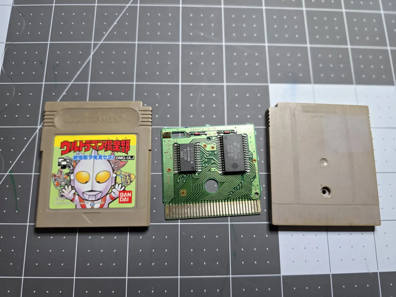
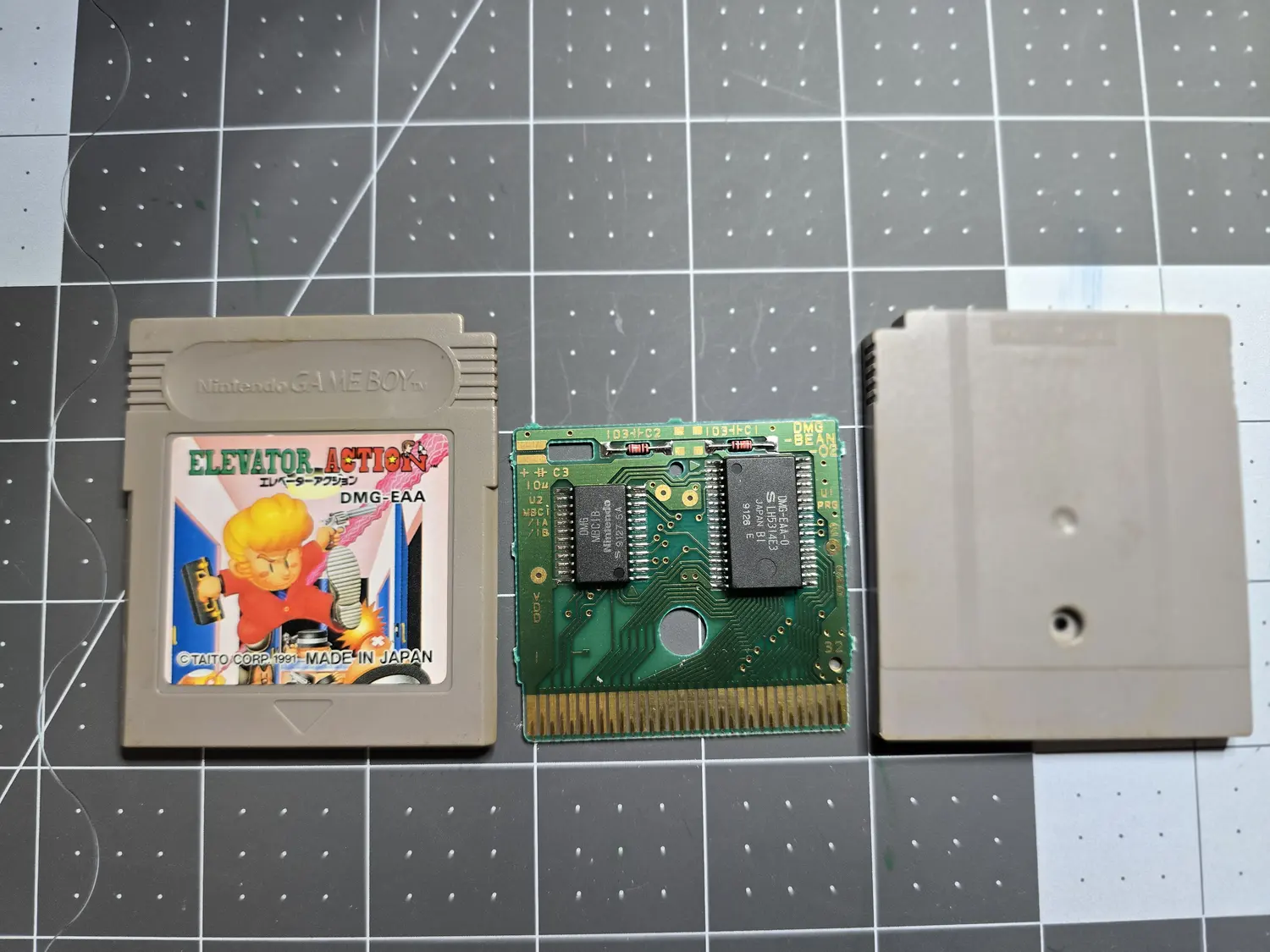
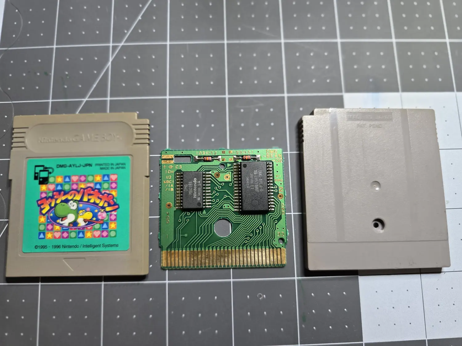
Why this matters on the bench: a rare cartridge can be repaired with a common donor. If the board is cracked, the edge connector is corroded past saving, or the mapper is dead, you do not need another copy of that game. You need any cheap cartridge on the same board, and you move the mask ROM across. The expensive part of a rare cart is the one chip that is least likely to fail.
Match the board, not the game. This is not one universal board: it is a family, and the differences are the things that change the circuit: a cart with battery-backed saves carries the SRAM, the battery and a different mapper, and larger or later games use MBC3 or MBC5 instead of MBC1. Read the designation off the donor board and match that. Two carts that look identical from the outside can be different boards inside.
When the cartridge’s own solder joints are the fault
There is a fault that sits between “the contacts are dirty” and “the mapper is dead,” and it is worth setting out carefully, because the version of it in circulation is more specific than the evidence behind it.
The claim is that the solder joints on a cartridge’s own chips crack with age and that reflowing them brings a dead game back. The broad version holds up. Several independent first-hand accounts describe a cart that would not boot, or that showed a white screen after the Nintendo logo, coming back after the chip legs were reflowed: the Game Boy Resource wiki, a UK repair guide, an iFixit thread, and Hungry Goriya’s write-up all report it working.
What none of them reports is how often it works. No sample counts, no success rate, and nobody says how many carts they opened where the joints turned out to be fine. Real, fixable, frequency unknown.
The mechanism, as asserted. Game Boy cartridge boards are 0.9 mm and flexible. Every insertion and removal flexes the board and stresses the IC legs, and the fractures that result are, in the wiki’s words, “just small enough to not be visible to the naked eye but big enough to cause electrical connectivity issues.” Three independent sources assert that mechanism. None demonstrates it. There is no cross-section, no failure analysis, no measurement anywhere. Treat it as the best available explanation rather than a settled one.
One useful thing does fall out of the flex model. If flex is what opens the joint, an unflexed board will not show the fault. The wiki makes the point directly: inspect with the game assembled and inserted in a console, because on the bench the board is not flexing and the fracture is closed. That is also what produces the works-if-I-press-it symptom, which is the strongest tell you get.
The same source gives the one search method I would actually trust: gently prod each leg on each chip and watch for movement. A properly soldered pin does not move. That is a mechanical test for a mechanical fault, and it beats staring at the joint, because with the board relaxed the fracture is closed and optical inspection is nearly useless.
Which chips, and the part I have to correct. I have heard this fault described, more than once, as the pins along the top edge of the board being the ones that go. I went looking for that and could not support it. Every repair source localises by chip and by board quadrant, never by pin number, pin row, or package edge: the mask ROM at U1, the mapper at U2, and on save-equipped boards the SRAM. The one account with enough positional detail to test the idea points the other way, since reflowing the top-left chip changed nothing and the bottom-right one fixed the cart.
The sources do not even agree on which chips. One names the mask ROM and the SRAM; the wiki names the mask ROM and the MBC, and the SRAM and MBC for corrupted sprites. That disagreement is the informative part. Nobody here is working from measured data, so treat “which chip” as a starting guess and let the symptom narrow it.
The only pin-specific instruction I found anywhere is to pay attention to pins 19 and 20 on an MBC3, and the reason given is functional rather than mechanical: that is where the real-time-clock crystal connects. If an MBC3 cart has lost its clock, that is a sensible place to look. It says nothing about mechanical stress.
One thing not to do with the pinout on this page. The 32-pin table in the pinout section is the gold edge fingers, per Pandocs. It is not a map of the chips. There is no published per-pin signal map for U1 or U2 on the DMG cartridge boards, and numbering a chip’s legs off the edge-connector table will have you probing the wrong pin entirely.
The edge-connector table does explain the symptom, though. Twenty-four of those 32 pins are address (6 to 21) or data (22 to 29) lines, so an open or intermittent connection anywhere on that bus corrupts fetched bytes rather than killing power. The boot ROM reads the logo back and compares it, which is why this failure class shows up as a garbled logo, or a logo that scrolls and then locks, instead of a dead console.
Where reflow belongs in the order: near the end. The wiki’s own does-not-boot list runs to eight steps and puts broken joints at seven. Dirty contacts, on the cart or in the console’s slot or both, are named the single most common cause. So:
- Try another game in the same console, and this cart in another console. That split alone tells you which side you are on.
- Remove and reinsert. Reseating fixes a surprising share of these.
- Clean the cartridge edge fingers, and clean the console slot. Both.
- Inspect for visible damage. Corroded or broken gold fingers are usually a dead cart.
- If the board has a save battery, take it off and look underneath before anything else. Electrolyte creep attacks traces and vias, and the legs can look perfect while the copper under the battery footprint is gone.
- Check continuity with a meter before you reach for the iron. A documented dead Super Mario Land turned out to be a fractured trace, cured with a jumper wire and no reflow at all. The owner proved it by holding the wire on with tape and watching the game boot.
- Only then suspect the joints.
If you do reflow it. Take the battery off first if one is fitted. The documented method is an iron rather than hot air: a knife or J tip, generous flux, and reflowing the solder that is already on the legs. Nobody sourced here prescribes adding fresh solder, doing both rows as a matter of course, or removing the chip. There is one hot-air account, at 225 to 250 C for at least 30 seconds behind a metal shield with a hole cut for the target chip, and its author explicitly warns readers off trying it. I would take that warning seriously: a blanket heat pass over a whole package is a blunt instrument on a part you cannot buy again.
Verifying it, which is where every account gets thin. Not one source describes an electrical check after the repair. Every documented success was declared on the cart booting once. That is a weak bar, and it is weakest for exactly this fault, because the fracture you are chasing is the kind that closes when the board is sitting still. Prod every leg again and confirm nothing moves, then reassemble, insert, and try to provoke the fault by pressing and flexing the cart in the slot. A cart that survives that is a repair. A cart that booted once on the bench is a coin toss.
A note on what is actually on these boards. The two-chip layout shown above is the simple case. A save-equipped board carries four: mask ROM at U1, mapper at U2, SRAM at U3, and a battery supervisor at U4. Read the designations off your own board rather than assuming, and check the cell while you are in there. Gekkio’s hardware database records the DMG-A02 board as taking a CR1616, not the CR2025 or CR2032 people tend to reach for.
SP won’t charge
On the SP, “no power” most often means “no charge.” The path is EXT2 port, then an EMI filter (EM8), then a fuse (F1), then the charger. Field experience is that EM8 most commonly fails on the ground side, disconnecting the EXT2 ground pin. Test order: insert the charger and look for ~5 V at the charger-IC 5 V pad; if it’s absent, continuity-check EM8 and then F1. Note for resale honesty: aftermarket SP cells are typically only 400 to 700 mAh whatever the label claims, and an SP won’t boot much below about 3.4 V at the pack.
Inside the family: what differs
A short tour of what the hardware is doing, which makes the faults above make sense. What I don’t list here is shared closely enough that it isn’t worth repeating per model.
- Two power generations. The 6 V DMG generation makes +5 V logic and roughly -18 V LCD bias from a flyback converter. The 3 V generation (Pocket, Light, Color) makes the same rails, or in the Color’s case +5 V plus a +13.6 V / -15 V pair, from half the input voltage. The GBA and SP move to a multi-rail switch-mode regulator with rails down to 1.8 V. Every generation uses a jack that mechanically lifts the battery when a plug is inserted, which is why an intermittent that only appears with a plug seated points at that switch.
- Video is direct-drive on the DMG generation. The SoC drives the panel’s shift registers directly, with no frame buffer or display controller in between. That is exactly why dead columns are a connection fault (a lost ribbon bond) and not a driver fault, and why no LCD bias (VEE) gives a white/blank screen even with perfectly healthy logic. The Color changed to an RGB panel with built-in drivers, so it has no contrast pot and no external bias ladder to blame. The Advance panel is reflective with no light source, which is the whole reason the mod market exists.
- The cartridge 5 V / 3.3 V boundary. The DMG, Pocket, Light and Color cartridge slots are 5 V logic. The GBA slot is 3.3 V in GBA mode and switches to 5 V in GB/GBC mode, selected mechanically by the cartridge’s own notch profile pressing a switch in the slot. This is the boundary that decides whether a flash cart needs level shifting, which is a topic I cover elsewhere.
- No region lockout, anywhere in this line, in the NES/SNES sense. Cartridge compatibility is purely about architecture (GB, GBC-only, or GBA), never region. Shell colour is the marker: a black cart shell is GB/GBC dual-compatible, a clear shell is GBC-only.
- The master clock is 4.194304 MHz on the DMG/Pocket/Light and, interestingly, on the Advance too (the AGB multiplies it by 4 for GBA mode and by 2 for GB/GBC mode). The Color runs an 8.4 MHz oscillator. One real DMG service trap: the crystal load capacitors are tied to the CPU die revision, so if you swap a CPU across revisions and leave the wrong load caps, you get marginal cold-start oscillator behaviour (works when warm).
Mods worth knowing
I do not reproduce anyone’s install guide here. This is an orientation to what is worth doing, and a few traps that cost real money on a resale build.
Fleet rules before any screen kit
Two rules that keep a build from eating its margin. Dry-test every screen kit before install, always. Socket the kit’s ribbon, power the bare board, run an actual cartridge, and inspect, because shipping damage is frequently invisible until first power-on and vendors void the return the moment you apply adhesive, peel film, or bend a ribbon. And assume the screen adhesive is permanent: on DMG and Pocket installs a botched alignment means buying a new panel, so use the alignment bracket and prefer Kapton over the supplied adhesive where the guides allow it.
Screens: the panel is the real taxonomy
Kit marketing names churn, but the underlying salvaged donor panel does not, and the panel tells you the image size, the scaling factor and most of the quirks. The current mainstream is the “Q5” panel (from a BlackBerry Q5), which gives a 4x integer scale on GB/GBC and supports convincing pixel-grid emulation. The older “9380” (BlackBerry Curve) panel was the long-time GBA gold standard but its stock is drying up. The cheap DSi-salvage (“ITA”) panels are 1x native, low power, and have a pronounced screen-door look like a stock AGS-101.
Two cross-cutting things to be able to explain to a buyer, because both generate returns:
- FRM (frame blending). GB and GBC games fake transparency by flickering sprites, relying on the awful response of the OEM panel to blur it. Modern panels are fast, so the sprite just visibly flickers on kits without frame blending. Titles it hits include Zelda: Link’s Awakening DX, F-Zero and ZAS. State whether a kit has FRM in the listing.
- The runtime hit. Every backlit kit costs battery. A DMG Q5 kit is roughly 25 to 50% of stock runtime depending on brightness, and the power-hungry GBC drop-ins are worse (one is called out as about a third of stock at minimum brightness). Plan a Li-ion or lithium-cell conversion into the same build, not as an afterthought.
For the GBA, identifying 40-pin vs 32-pin first is mandatory, because it decides either what you buy or how you install it. For the SP, all 32-pin AGB kits are electrically compatible with the SP through a passive 32-to-34-pin adapter, but the AGS-001 front-light and AGS-101 back-light supplies are not interchangeable, so an in-console light swap is variant-specific. One GBC-specific install trap cracks panels: flush-cut the cartridge-connector pin tails (and watch the battery-clip BT+ pin) before a GBC IPS install, or an untrimmed pin destroys the new ribbon on reassembly.
Backlight and bivert (DMG, Pocket)
The cheap path that keeps the OEM panel’s look. You remove the rear reflective film, put an LED panel behind the LCD, and add a “bivert” (a 74HC04 hex inverter tapping the two LCD data lines) to sharply raise contrast. One thing worth knowing if you sell one: at least one common bivert module ships with its unused inverter inputs left floating, which wastes a few milliamps and makes heat. Unlikely to damage the console, but tie the unused inputs off or use a properly terminated board. A bivert does nothing useful behind a replacement IPS panel (it will only invert the colours), so don’t sell it as an upgrade on an IPS build.
Audio, power and video-out
RetroSix’s CleanAmp line amplifies the original audio to modern levels, but on a GBA their own warning is that CleanAmp alone makes hum and hiss noticeably worse, so budget CleanAmp plus their Dehum board together, not the amp alone. For power, the mature paths are USB-C: a drop-in Li-ion module for most models, a straightforward EXT2-pin USB-C charge board for the SP, and dongle or port-replacement options for the barrel-jack models. On video-out, the ranking is that a dedicated consolizer (a real AGB mainboard plus an FPGA board out to HDMI) beats every in-console HDMI kit on scaling and audio.
Flash carts and saves
For resale honesty, two things matter. Clone flash carts are everywhere (sold as “GB Pro+” and similar), usually identifiable by an Altera CPLD instead of the Lattice FPGA in a genuine EverDrive, and updating a clone with official firmware can brick it. If a unit ships with a flash cart, disclose whether it’s genuine. And dump the cartridge save with a GBxCart-class tool before you replace a dead save cell, so the save survives the battery swap.
What actually changes value
The screen kit is the headline, so name the panel and whether it is laminated, because that is what enthusiast buyers filter on. State FRM and state the runtime hit. Reversibility sells: a solder-free, cut-free build on an OEM shell is worth more than a trimmed original, and if you do use an aftermarket IPS-ready shell, keeping the original shell with the unit is the higher-value move. And describe the recap accurately: a “fully recapped” claim on a model that doesn’t need one (the SP, for instance) is the kind of thing that gets noticed.
Recap and parts
The one rule to carry away: identify the exact board before you order, because the parts are not uniform even within a model.
The DMG DC-DC converter is the one place a generic cap kit gets you the wrong part. The converter’s capacitor complement genuinely changes across revisions: the early A/B boards use a 10 uF output bulk cap where the later C/D boards use 100 uF, a tenfold difference. Read the cans on the board before ordering. If you stock 33 uF 25 V, 100 uF 10 V, 22 uF 25 V and 10 uF 16 V you cover every DMG converter revision. The rest of the DMG is spread across the LCD board (note the five 1 uF caps that sit under the LCD module: don’t lift the module, solder replacements to the cut legs, and modern kits ship ceramics for these five), the mainboard, and the passive headphone jack board.
For the SMD models, the values by model:
- Pocket / Light, a handful of SMD aluminium caps. Watch that the Light’s C29/C32 do not match the Pocket’s despite sharing designator numbers, so never order Light caps off a Pocket list.
- Color, three: C32 (100 uF, power), C35 (22 uF, LCD), C38 (100 uF, audio).
- Advance, four (CP1 to CP4). Two worth flagging: CP2 wants a low-ESR part because it’s a boost-converter output, and CP3 is 470 uF, whose off-the-shelf aluminium equivalent is unusually tall for a thin console, so a low-profile polymer or tantalum is the routine field answer there. On resale work be aware tantalum fails short and these sit on power rails, so I lean toward aluminium or polymer on a console I’m selling.
- Advance SP, one (CP1, 100 uF).
The pragmatic path for throughput is a pre-matched kit per model, because the vendor has already solved the footprint problem. The standing rule, worth restating because it’s where most amateur recaps go wrong: replace with equal capacitance and equal-or-greater voltage, and prefer the higher temperature rating.
Some parts are effectively unobtainium new: the DMG’s Sharp audio amp (IR3R40) and LCD regulator (IR3E02) ASICs have no modern drop-in, so it’s salvage from a donor or a board-level replacement (RetroSix’s CleanPower replaces the whole DMG converter board, CleanAmp replaces the audio path). On a fleet, your worst board is your parts stock. Full BOMs, real distributor part numbers and footprint dimensions live in my bench notes; the summary above is enough to order against once you’ve read the board.
A note on the Game Boy Micro (OXY-001)
My documentation on the Micro is thin: no service manual, no schematic, no board scan, and only a handful of surveyed units. So treat this as provisional rather than bench-proven. The one fact that changes every buying decision: the Micro plays Game Boy Advance cartridges only. It dropped backwards compatibility entirely, so no original Game Boy or Game Boy Color games at all. It brings back a real 3.5 mm headphone jack (unlike the SP), combines its link and charge ports into one proprietary connector, and uses a small, fine-pitch backlit screen whose OEM replacements are rare and expensive enough that a damaged Micro panel is usually not worth fixing. Some Micros, particularly silver ones, suffer the same brittle-plastic frame problem as late AGS-101 shells, so check the frame before quoting any work that flexes it.
The hard data behind all of the above (the per-board cap maps with the substitutes I fit, the non-cap consumables, the chip and connector pinouts, and the schematic facts) is tabled in the sections that follow. It is organised by board revision, because that is what actually decides the job. Long per-item notes fold away to keep it readable; expand any of them for the full detail.
Capacitor lists
Per board revision, not per model. The DMG splits its electrolytics across four separate PCBs with independent revision runs, so order by board or you will end up short, and read the DC-DC board’s silkscreen before you order, because C5 differs by a factor of ten between revisions.
DMG-CPU-01-05 DMG-01 mainboard, revisions -01 to -05 - replaceable SoC and RAM, no per-revision cap map published (use the -06 list and read the board)
Board p/n: Nintendo 18392 PCB ASSEMBLY, CPU
DMG-CPU-06 DMG-01 mainboard rev -06 - the long-run revision, and the one with a traced schematic and a published cap map
Board p/n: Nintendo 18392 PCB ASSEMBLY, CPU
Mainboard — electrolytics
| Desig | Value | V | OEM p/n | Substitute | Note |
|---|---|---|---|---|---|
| C1 | 100 uF | 10 V | EEU-FR1A101 (100 uF 10 V, 5 x 11 mm, 2.0 mm pitch) | VDD bulk, power sheet ✓dmg-sch,console5,retrosix | |
| C2 | 100 uF | 10 V | EEU-FR1A101 | VCC bulk, power sheet ✓dmg-sch,console5 | |
notes on C2Worth knowing before you go hunting: RetroSix’s DMG-CPU-06 table
names this second 100 uF/10 V cap C7, not C2. The traced
schematic and Console5 both say C2, and a schematic outranks a
wiki table, so C1/C2 is the call - but the count is identical
either way, so it costs nothing in the BOM. Just do not look for a
C7 that is not on your board. | |||||
| C3 | 1 uF | 50 V | 1 uF 50 V X7R MLCC, 0805 or 1206 - no Panasonic FR part exists at this value | audio AC coupling, right ✓dmg-sch,console5 | |
| C4 | 1 uF | 50 V | 1 uF 50 V X7R MLCC, 0805 or 1206 | audio AC coupling, left ✓dmg-sch,console5 | |
| C5 | 10 uF | 16 V | EEU-FR1H100 (10 uF 50 V) | amp bootstrap/bias on HPLBC ✓dmg-sch,console5 | |
| C6 | 10 uF | 16 V | EEU-FR1H100 (10 uF 50 V) | amp bootstrap/bias on HPRBC ✓dmg-sch,console5 | |
DMG-CPU-07/08 DMG-01 mainboard rev -07 / -08 - cost-reduced, SoC and both RAM dies are glop-top epoxy and therefore unreplaceable
Board p/n: Nintendo 18392 PCB ASSEMBLY, CPU
DMG-LCD-06 DMG-01 LCD / control board rev -06 - the long-run LCD board (fitted from DMG-CPU-03 onward). Note DMG-LCD-04 has never been observed; the run goes -03 to -05
LCD / control board — electrolytics
| Desig | Value | V | OEM p/n | Substitute | Note |
|---|---|---|---|---|---|
| C1 | 100 uF | 10 V | EEU-FR1A101 | ✓dmg-lcd-sch,console5,retrosix | |
| C2 | 100 uF | 10 V | EEU-FR1A101 | ✓dmg-lcd-sch,console5,retrosix | |
| C3 | 10 uF | 25 V | EEU-FR1H100 (10 uF 50 V) | ✓dmg-lcd-sch,console5,retrosix | |
| C6 | 1 uF | 50 V | 1 uF 50 V X7R MLCC, 0805 or 1206, fitted leg-to-leg | one of the five that sit UNDER the LCD module ✓dmg-lcd-sch,console5,retrosix | |
notes on C6C6 to C10 sit under the LCD module and cannot be desoldered
without lifting it. Do not lift it. Console5’s own guidance is to
cut the leads as close to the old capacitor body as possible and
solder the replacements to the old legs, because the LCD modules
are known for developing bad connections and you do not want to
aggravate one during a recap. Their kit has shipped ceramic
replacements for these five specifically since 2023, and for a
refurb-for-resale unit that is the right call: a 1 uF 50 V X7R
MLCC has better ESR and an indefinite shelf life, and there is no
bulk-storage requirement at that position. | |||||
| C7 | 1 uF | 50 V | 1 uF 50 V X7R MLCC, fitted leg-to-leg | under the LCD module ✓dmg-lcd-sch,console5,retrosix | |
| C8 | 1 uF | 50 V | 1 uF 50 V X7R MLCC, fitted leg-to-leg | under the LCD module ✓dmg-lcd-sch,console5,retrosix | |
| C9 | 1 uF | 50 V | 1 uF 50 V X7R MLCC, fitted leg-to-leg | under the LCD module ✓dmg-lcd-sch,console5,retrosix | |
| C10 | 1 uF | 50 V | 1 uF 50 V X7R MLCC, fitted leg-to-leg | under the LCD module ✓dmg-lcd-sch,console5,retrosix | |
DC-CONV-A/B DMG-01 DC-DC converter, rev A / B - input LC filter, 2SD1328 control transistor, 10 uF output cap, NO undervoltage lockout
Board p/n: Nintendo 18393 / 18486 PCB ASSEMBLY, DC/DC CONV
DC-DC converter daughterboard — electrolytics
| Desig | Value | V | OEM p/n | Substitute | Note |
|---|---|---|---|---|---|
| C4 | 33 uF | 25 V | EEU-FR1V330 (33 uF 35 V) | same on every DC-CONV revision ✓dcconv-ab,console5 | |
| C5 | 10 uF | 10 V | EEU-FR1H100 (10 uF 50 V) | TENFOLD different from rev C/D - do not order a generic 'DMG DC-DC cap kit' without knowing the revision single sourcedcconv-ab | |
notes on C5This is the one position in the whole DMG BOM where a vendor cap
list will hand you the wrong part. Rev A/B is 10 uF here; rev C
and rev D are 100 uF. Console5’s list is a deliberate superset of
all variants with designators marked N/A, so it is not telling you
which one your board wants. Read the silkscreen, or just read the
cans. | |||||
DC-CONV-C DMG-01 DC-DC converter, rev C - input filter without L1, 2SC2412 control transistor, 100 uF output cap, still no UVLO
Board p/n: Nintendo 18393 / 18486 PCB ASSEMBLY, DC/DC CONV
DC-DC converter daughterboard — electrolytics
DC-CONV2-D DMG-01 DC-DC converter, rev D (DC-CONV2) - the only DMG converter with an undervoltage-lockout block, and the only one with a third electrolytic
Board p/n: Nintendo 18393 / 18486 PCB ASSEMBLY, DC/DC CONV
DC-DC converter daughterboard — electrolytics
| Desig | Value | V | OEM p/n | Substitute | Note |
|---|---|---|---|---|---|
| C4 | 33 uF | 25 V | EEU-FR1V330 (33 uF 35 V) | ✓dcconv-d,console5 | |
| C5 | 100 uF | 10 V | EEU-FR1A101 (100 uF 10 V) | single sourcedcconv-d | |
| C6 | 22 uF | rating not printed on the sheet | EEU-FR1H220 (22 uF 50 V) - fit 16 V or higher | part of the UVLO block; exists ONLY on rev D single sourcedcconv-d,retrosix | |
notes on C6The rev-D sheet does not print a voltage rating for C6. RetroSix
give 22 uF 10 V for the position, which is a single source and a
marginal rating on a nominal-6 V input rail, so I fit 16 V or
25 V and stop worrying about it. | |||||
DMG-JACK DMG-01 headphone-jack board - revisions 01 / 02 / 03 are drawn on one schematic sheet and are not electrically distinct
Board p/n: Nintendo 18395 PCB ASSEMBLY, AUDIO JACK
Headphone-jack board — electrolytics
| Desig | Value | V | OEM p/n | Substitute | Note |
|---|---|---|---|---|---|
| C1 | 100 uF | 6.3 V | EEU-FR1A101 (100 uF 10 V) - there is no 100 uF 6.3 V FR part | AC coupling + filter, one per channel ✓dmg-jack-sch,console5,retrosix | |
| C2 | 100 uF | 6.3 V | EEU-FR1A101 (100 uF 10 V) | AC coupling + filter, one per channel ✓dmg-jack-sch,console5,retrosix | |
notes on C2The board also carries L1/L2/L3 = 3.3 uH series inductors, which
do not need replacing but do get destroyed by careless rework.
L3 is on the ground return. | |||||
MGB-xCPU Game Boy Pocket (MGB-001) mainboard - MGB-CPU-01, MGB-ECPU-01, MGB-LCPU-01 and -02, drawn together as MGB-xCPU. The 'L' tracks the power LED, which early Pockets omitted
Mainboard — electrolytics
| Desig | Value | V | OEM p/n | Substitute | Note |
|---|---|---|---|---|---|
| C29 | 33 uF | 25 V | EEE-FK1E330UR (5.0 x 5.8 mm - prefer this over the 6.3 mm FK1E330P) | LCD bias / VEE inverter. WARNING: the Light's C29 is a different part ✓mgb-sch,console5,retrosix | |
notes on C29The Pocket and the Light share designator numbers but not values
at C29 and C32. Never order Light caps off a Pocket list. | |||||
| C30 | 330 uF | 6.3 V | EEE-FK0J331P (8.0 x 6.2 mm) | main bulk. Console5 writes '6v'; the schematic settles it at 6.3 V ✓mgb-sch,console5,retrosix | |
notes on C30Stock trap I hit on 2026-07-19: DigiKey had only 71 units of
EEE-FK0J331P against 20,230 of the 100 uF 6.3 V. If you are
batching Pockets, buy that value deep or you will stall mid-run. | |||||
| C31 | 100 uF | 6.3 V | EEE-FK0J101UR (5.0 x 5.8 mm) | audio - the classic low or no speaker output when it fails ✓mgb-sch,console5,retrosix | |
| C32 | 100 uF | 6.3 V | EEE-FK0J101UR | DC-DC output filter. The Light's C32 is 330 uF, not this ✓mgb-sch,console5,retrosix | |
MGL-CPU-01 Game Boy Light (MGB-101) mainboard - the single board revision, Japan-only, AA cells, electroluminescent panel with a Mitsumi inverter transformer at T1
Mainboard — electrolytics
| Desig | Value | V | OEM p/n | Substitute | Note |
|---|---|---|---|---|---|
| C29 | 1 uF | 35 V | no MPN recorded - the Pocket's 33 uF 25 V part is NOT a substitute | power sheet. The Pocket's C29 is 33 uF 25 V - completely different part at the same designator ✓mgl-sch,console5 | |
| C30 | 330 uF | 6.3 V | EEE-FK0J331P | power sheet ✓mgl-sch,console5 | |
| C31 | 100 uF | 6.3 V | EEE-FK0J101UR | analog audio sheet ✓mgl-sch,console5 | |
| C32 | 330 uF | 6.3 V | EEE-FK0J331P | power sheet. The Pocket's C32 is 100 uF - do not cross the lists ✓mgl-sch,console5 | |
| C38 | 33 uF | 25 V | EEE-FK1E330UR | power sheet ✓mgl-sch,console5 | |
notes on C38Non-electrolytic parts on the Light’s power sheet that sit in the
failure path and are orderable: F1 1 A and F2 1.2 A fuses,
Q3 2SD1781K, D2 MA2J111, D3 Schottky, T1 the DC-DC transformer,
C34 220n, C36 10n, C39 15n, C33 6.8u. RetroSix have no Game Boy
Light page at all - Japan-only model, outside their catalogue - so
Console5 plus the schematic is the whole documentary picture here. | |||||
CGB-CPU-01-03 Game Boy Color, CGB-CPU-01 to -03 - SoC steppings A/B/C, the ones with audio-register bugs and higher background noise. CPU-01 has NO number under the left battery spring; an absent number IS the ID
Mainboard — electrolytics
| Desig | Value | V | OEM p/n | Substitute | Note |
|---|---|---|---|---|---|
| C32 | 100 uF | 6.3 V (OEM can 6.3 x 5.4 mm) | EEE-FK0J101UR (5.0 x 5.8 mm) | unit will not power on when this one fails - the highest-yield single cap in this whole family ✓cgb-sch,console5,retrosix,silvestron | |
notes on C32A dead-on-arrival GBC with clean battery terminals is C32 far more
often than anything else. The schematic prints
C32 100uF/6.3V(o6.3x5.4), which settles Console5’s ambiguous
“6v” as 6.3 V and gives the OEM can size; silvestron’s independent
tech doc agrees on both. | |||||
| C35 | 22 uF | 16 V (OEM can 4.0 mm diameter) | EEE-FK1C220UR (4.0 x 5.8 mm) - NOT the 5.0 mm EEE-FK1C220R | dim or low-contrast screen ✓cgb-sch,console5,retrosix,silvestron | |
notes on C35The schematic annotates
| |||||
| C38 | 100 uF | 4 V (OEM can 5.2 x 5.4 mm) | EEE-FK0J101UR (6.3 V is fine electrically) | quiet or crackling audio ✓console5,retrosix,silvestron | |
CGB-CPU-04/05 Game Boy Color, CGB-CPU-04 / -05 - SoC stepping C or D. Revision D fixes most of the audio problems but introduces a PPU TILE_SEL bug, and a -04 board can carry either C or D, which you can only settle by opening it
Mainboard — electrolytics
CGB-CPU-06 Game Boy Color, CGB-CPU-06 - SoC stepping E, work RAM integrated into the die so U2 is ABSENT. Electrically the cleanest GBC to refurbish for resale
Mainboard — electrolytics
AGB-CPU-01-04 Game Boy Advance, AGB-CPU-01 to -04 - 40-pin LCD connector. The revision digits are visible through the battery-cover clip hole; first digit '0' means 40-pin
Mainboard — electrolytics
| Desig | Value | V | OEM p/n | Substitute | Note |
|---|---|---|---|---|---|
| CP1 | 100 uF | 4 V | EEE-FK0J101UR (6.3 V is fine here) | input bulk, immediately before U4 Vin ✓agb-sch,console5,retrosix | |
| CP2 | 100 uF | 6.3 V, LOW-ESR | low-ESR 100 uF 6.3 V, or a polymer - a generic part here is a downgrade | boost-converter output. Nintendo annotates this position '(LOW Z)' on the schematic ✓agb-sch,console5,retrosix | |
notes on CP2The “(LOW Z)” annotation is an OEM specification, not a
suggestion, and no vendor cap list I have seen carries it. A
generic 100 uF 6.3 V on a boost-converter output is a real
downgrade. | |||||
| CP3 | 470 uF | 6.3 V | 470 uF polymer or low-profile tantalum. The FK part (EEE-FK0J471P) is 8.0 x 10.2 mm - measure your headroom first | main bulk - the height trap in this whole BOM ✓agb-sch,console5,retrosix | |
notes on CP3EEE-FK0J471P is 10.2 mm tall, taller than it is wide, and the AGB
is a thin console. FK has no lower-profile 470 uF 6.3 V at
all - the 6.3 V block runs 100/220 uF in case D, 330 uF in D8 or
E, then jumps straight to 470 uF in case F at 8.0 x 10.2. Several
vendor kits ship a 470 uF 10 V tantalum (marked 477A, 7343/D case,
about 2.8 mm tall) for this position, which is the routine field
answer. My caveat for resale work: tantalum fails short and
this sits on a power rail, so on a console I am selling I lean
polymer or aluminium. | |||||
| CP4 | 100 uF | 4 V | EEE-FK0J101UR | audio amplifier ground reference - why a humming or hissing GBA is worth a recap even when the rails look fine ✓console5,retrosix | |
AGB-CPU-10 Game Boy Advance, AGB-CPU-10 - 32-pin LCD connector, lower LCD current draw and longer battery life. First digit '1' means 32-pin
Mainboard — electrolytics
| Desig | Value | V | OEM p/n | Substitute | Note |
|---|---|---|---|---|---|
| CP1 | 100 uF | 4 V | EEE-FK0J101UR | input bulk ✓agb-sch,console5,retrosix | |
| CP2 | 100 uF | 6.3 V, LOW-ESR | low-ESR 100 uF 6.3 V or polymer | boost-converter output, OEM-annotated '(LOW Z)' ✓agb-sch,console5,retrosix | |
| CP3 | 470 uF | 6.3 V | 470 uF polymer or low-profile tantalum - check headroom before ordering the 10.2 mm aluminium | main bulk ✓agb-sch,console5,retrosix | |
| CP4 | 100 uF | 4 V | EEE-FK0J101UR | audio amp ground reference ✓console5,retrosix |
AGS-CPU-01-21 Advance SP (AGS-001), boards C/AGS-CPU-01 / -11 / -21 - discrete power regulator at U4 with battery VCC on pin 4, discrete IR3R60N amp at U3, 16-pin MM1581A charger
Mainboard — electrolytics
| Desig | Value | V | OEM p/n | Substitute | Note |
|---|---|---|---|---|---|
| CP1 | 100 uF | 4 V | EEE-FK0J101UR (6.3 V) | the ONLY aluminium electrolytic on the SP mainboard, under the volume slider ✓ags-sch,console5,retrosix | |
notes on CP1Triple-sourced and worth internalising because it is
counter-intuitive and it saves bench time: everything else on the
SP mainboard is ceramic or tantalum and does not age out.
“Recap the SP” is a one-capacitor job. If the fault survives CP1,
it is not a capacitor fault - go to the charge circuit or the
rails. | |||||
AGS-CPU-30 Advance SP (AGS-001), board C/AGS-CPU-30 - the last revision, ICs consolidated into the Mitsumi PM B3. Battery VCC enters on U3 pin 36, not U4 pin 4
Mainboard — electrolytics
AGT-CPU-01 Advance SP (AGS-101, back-lit), board C/AGT-CPU-01 - the only AGS-101 board, and there is NO schematic for it anywhere. AGS-001 and AGS-101 boards are not interchangeable
Mainboard — electrolytics
| Desig | Value | V | OEM p/n | Substitute | Note |
|---|---|---|---|---|---|
| CP1 | 100 uF | 4 V | EEE-FK0J101UR | the only aluminium electrolytic on the board ✓console5,retrosix | |
notes on CP1For an AGS-101 charge or rail fault the AGS-CPU-11 sheets are an
analogue, not ground truth - no AGT-CPU-01 schematic exists in
any source I have found. Telling a 101 from a 001 without opening
it: press the brightness button. If the light turns off completely
it is an AGS-001; if it only gets brighter and never turns off it
is an AGS-101. The rear label is the least trustworthy test,
because aftermarket shells are overwhelmingly sold with AGS-001
labels, so a reshelled 101 reads “001”. | |||||
Replacement parts
The non-cap parts a Game Boy repair actually consumes, and the handful that are donor-harvest only.
Non-cap consumables
| Function | OEM part | Why replaced | Substitute | Note |
|---|---|---|---|---|
| DMG DC-input protection diode D1 | RB100A, 1 A Schottky (Nintendo part 18388, on the CPU board) | a DMG that is dead on the barrel jack but fine on batteries is a D1 check before anything else | SB160 (1 A / 60 V Schottky barrier) - the vendor-documented cross | in series with the whole supply, so its forward drop comes out of your headroom ✓tm91,silvestron,dmg-sch |
notesConfirmed as a discrete line item with its own Nintendo part number and
quantity in the CPU PCB assembly parts list, and independently by
silvestron’s DMG-01 board map ( Design consequence for dongle work: because D1 blocks rather than shunts a reversed supply, a centre-positive plug typically gives a dead-but-undamaged console. And because it is in series, design a dongle to the +6 V nominal, not to the bottom of the 3.5-7.0 V window. | ||||
| DMG DC-DC main switching transistor Q1 | 2SD1664R (identical on every DC-CONV revision) | the switch in the self-oscillating flyback; dead means no +5 V and no -18 V | obsolete Japanese part - substitute must match Vceo, hFE and switching speed, or replace the board | RetroSix's CleanPower replaces the whole daughterboard as a four-wire swap ✓dcconv-ab,dcconv-c,dcconv-d,retrosix |
notesOn any DMG whose DC-DC board has leak damage under it, a board-level
replacement is cheaper in bench time than sourcing a 2SD1664R and a
33 uF. There is also no orderable substitute for the transformer T1, so a
dead transformer means a donor board or a board swap either way. | ||||
| DMG DC-DC control transistor Q2 | 2SD1328 on rev A/B; 2SC2412 on rev C and D | control-loop fault | commodity NPN substitution is usually workable for the 2SC2412 | READ THE BOARD - this part genuinely changes between revisions single sourcedcconv-ab,dcconv-c,dcconv-d |
notesThe A/B-versus-C/D split is Gekkio’s traced schematics only; neither
Console5 nor RetroSix breaks the DC-DC board down to semiconductor level.
If you are salvage-matching a control transistor, read the board, not the
table you remembered. | ||||
| DMG DC-DC UVLO digital transistors (rev D only) | DTC143T x3 (Q3/Q4/Q5), with D5 3.3 V zener and R6/R7/R8 | part of the undervoltage-lockout block that exists only on DC-CONV2 rev D | DDTC143TCA-7-F (Diodes Inc, SOT-23-3, 50 V / 100 mA, R1 = 4.7 k, no R2) | the one DC-DC semiconductor you can still buy new. Order the -F (lead-free) suffix; the plain DDTC143TCA-7 is discontinued single sourcedcconv-d |
notesROHM’s DTC143T is an NPN pre-biased transistor with a 4.7 k series base
resistor and no base-emitter resistor, which matches the Why this matters beyond the part: a rev-D board will cleanly refuse to start on a sagging supply where an A/B/C board would brown out and put garbage on the LCD. If a DMG on a variable bench supply goes hard-dead below a threshold instead of degrading, that is the UVLO working, not a fault. If a dongle boots one DMG and not another, check which DC-DC revision is fitted before you suspect the dongle. The actual threshold is not printed on the sheet - measure it, do not assume it. | ||||
| DMG volume potentiometer RV1 | 10 kOhm x 2 dual-gang thumbwheel, 5-pin (marked B103) | scratchy or crackling volume - the single most common misattribution in the DMG audio complaint pile | replacement sold by HandHeldLegend, Console5, RetroModding, ZedLabz | a $3 part, not a cap fault ✓dmg-sch,console5 |
notesThe same physical part serves the GBA’s single-gang application if you
parallel the gangs - HandHeldLegend’s listing says to solder pins 2 and 3
together and pins 4 and 5 together for GBA use. That pin mapping is their
instruction alone; the 10 k value is confirmed by the schematic and by the
vendor listings. | ||||
| DMG LCD-board contrast pot VR1 | 30 kOhm (DMG-LCD-06) | worn or dirty pot gives wandering contrast; feeds the IR3E02's VR pin through J2 | 30 k pot, same footprint | the Color's equivalent is 50 k - do not carry pots across models single sourcedmg-lcd-sch |
| Pocket / Light LCD bias pot VR2 | 30 kOhm (both MGB and MGL regulator sheets) | drifting contrast | 30 k pot | both boards agree on the value; the Color does not ✓mgb-sch,mgl-sch |
| Color interlace / bias pot VR2 | 50 kOhm | visible horizontal interlace on static graphics | 50 k pot | Console5 report that tuning VR2 eliminates static-image interlace - worth trying on a refurb before condemning the panel single sourcecgb-sch,console5 |
notesThis is Console5’s claim, not my measurement, but it costs nothing to try
and it is a real service adjustment rather than a factory-only trim. | ||||
| GBA fuse F1 | Littelfuse 04341.25 (1.25 A, 32 V, 0603, marking code J, fast-acting) | dead, no power at all | Littelfuse 04671.25, or Bourns SF-0603FP125F-2 (0603, 1.25 A, fast-acting) | fit fast-acting, not slow-blow - this fuse is the only thing between a shorted rail and the CPU ✓agb-sch,retrosix |
notesThe schematic label 4341.25 is one token, not two fields: it is the OEM
part number itself, a member of Littelfuse’s 434 thin-film chip-fuse
series, which is fast-acting throughout. The sibling convention
(0434.500, 0434.750, 0434002, 0434003) settles the reading. | ||||
| GBA off-state discharge resistor R13 | 150 Ohm | console will not reboot if power-cycled inside about ten seconds | 150 ohm chip resistor | an easy fault to misread as a dead regulator ✓agb-sch,retrosix |
notesWith the switch off, R13 shunts the rail capacitors to ground so they
discharge fast. If R13 is missing or damaged, or the switch’s OFF contact
is dirty, the caps stay charged, the system stays in a non-resettable
state, and a quick off-then-on fails to boot while a ten-second wait works
fine. Do not chase that as a regulator fault. | ||||
| GBA power switch | - | dead, intermittent, or the R13 symptom above; also a documented source of audio grime | a Nintendo DS Lite power switch is a direct functional replacement (RetroSix) | DSL switches are cheap and abundant; GBA-specific ones are not single sourceretrosix |
| SP EXT2 EMI filter EM8 | 4-pin common-mode filter on the EXT_VIN path | no charge | field-expedient fix is to remove it and bridge with wire, accepting some audio noise while charging | RetroSix report it most commonly fails on the ground side; test continuity 1-2 and 3-4 single sourceags-sch,retrosix |
notesThe topology is confirmed on the schematic; the failure-frequency claim is
RetroSix’s, not my count. | ||||
| SP charge-path fuse F1 | 0603 fuse on EXT_VIN | no charge | RetroSix recommend a resettable (PPTC) 0603 | single sourceags-sch,retrosix |
| DMG audio amplifier IC | Sharp IR3R40 / IR3R40N (U4, Nintendo part 18370) | dead or distorted audio that survives a recap and a pot clean | no modern drop-in - salvage from a donor, or bypass the whole path with a board-level amp | unobtainium new. The Pocket/Light IR3R53N is NOT a substitute - different pinout ✓tm91,dmg-sch,console5 |
| LCD bias regulator IC | Sharp IR3E02 (DMG-REG) on DMG/Pocket/Light; CGB-REG (Console5: IR3E06N) on Color | no image, or bias rails wrong with a good DC-DC | no modern drop-in - donor harvest, or replace the whole power board | unobtainium new; budget for donor consoles as a standing line item, not an exception ✓dmg-lcd-sch,cgb-sch,console5 |
notesNone of the IR3-series ICs are purchasable new. On a fleet, your worst
board is your parts stock. | ||||
| DMG battery contacts | five terminals: 2 soldered to the PCB, 3 slid into the back shell | alkaline leak damage - the classic DMG job | full kits from RetroModding; separate shell-spring and PCB-spring sets from RetroSix, HandHeldLegend, RetroGameRepairShop | Pocket, Light and Color each have 2 soldered + 1 in the shell, not 2 + 3 ✓consolemods |
notesThis is the detail that catches people ordering: a “battery contact set”
that is shell-only will not fix a corroded PCB terminal, and the DMG’s
split is different from every later model’s. | ||||
| Speakers | - | blown or rattling speaker | FunnyPlaying clear speaker, or unbranded generics; all two-wire solder-in, no connector | the Color, Pocket and Light SHARE one speaker - one SKU covers three models. DMG, AGB and AGS each take their own ✓consolemods |
| Cartridge save cells | CR2025 on most GB/GBC carts (a few CR2032 and CR2016); CR1616 near-universally on GBA carts | lost saves | tabbed cells, or spot-weld tabs on | hot-swapping the cell with the cart powered in a running console preserves the existing save ✓consolemods |
notesCounted from ConsoleMods’ per-title tables: the GBA list is 252 CR1616
entries with no other type; the GB list is 13 CR2025, 2 CR2032, 2 CR2016.
Worth knowing: many late-production SRAM titles shipped with FRAM
substituted at the factory, and FRAM is functionally identical to
battery-backed SRAM from the console’s side, so a converted cart never
needs a cell again. | ||||
| SP battery pack (AGS-003) | AGS-003 | swollen or dead pack - routine on a 20-year-old SP, not exceptional | named vendors only (HelderGameTech MegaBat800, Mahko/RetroModding); ConsoleMods measured cheap generics at about 350 mAh actual | assume marketplace capacity claims on AGS-003 clones are fabricated ✓consolemods |
notesI could not verify the OEM pack’s own rating: search results give 850 mAh
at 3.7 V, 900 mAh at 3.6 V and 850 mAh at 3.8 V, all from retail listings
and none from Nintendo. I do not quote a capacity figure for the OEM pack
in a listing. | ||||
| Fasteners and drivers | Tri-Point Y0 outer shell across the line; JIS J0 internal | stripped screws are a visible defect on a resale unit | real J0 driver - a Phillips engages JIS screws but cams out and strips them | cartridges change families: 3.8 mm gamebit on GB/GBC carts, Tri-Point Y0 on GBA carts ✓consolemods |
Chip & connector pinouts
The component library: each IC and connector defined once, with an interactive pin diagram and a folded pin table. The revision badge on each card shows which board revision(s) it applies to. Where I could not verify a pinout against a schematic or manual on my disk, the card says so and the table is empty.
Components & pinouts
Each part is defined once. The revision badge on every card shows exactly which board revision(s) it applies to.
Every diagram rotates and flips to match the board in front of you, zooms from a whole-package overview up to 3.2×, and saves at the orientation you are looking at — ↓ SVG matches the screen, and ↓ SVG (print) gives you the same drawing as ink on white. Both are vector, so print them at any size you like, which is the better route for the long connector pinouts since printing this page has to shrink them to fit the sheet. The # beside a part name links to that card, and the one in the pin panel links to a single pin — either link opens the card for whoever you send it to.
Advance main power IC U4 - Mitsumi MM1514X / Seiko S-6960E / ROHM 9750A / 9750B AGB-CPU-01-04 · AGB-CPU-10 sop-16single sourceagb-sch,gbasm,gbhwdb#
the IC that makes every rail on a GBA - one shorted output takes all of them down. Pin numbers are from the schematic scan only
The service manual states plainly that the 3 VDC from the two AA cells “is converted by the U4 power IC to supply the system”, and the schematic draws U4 as the 16-pin part below, so U4-is-the-power-IC is solid. The pin numbering comes from the one schematic scan, so it carries the lower tag.
Several second-source vendors filled this socket over the production run (Mitsumi, Seiko, ROHM), so match the marking on the actual board before ordering a replacement.
The input chain into pin 1, and where a no-power hunt starts: F1 fuse (Littelfuse 04341.25, 1.25 A fast) -> power switch SW1 -> R13 150 ohm -> CP1 100 uF/4 V -> U4 Vin.
RetroSix report that the regulator has over-current shutdown across all outputs, so one shorted rail kills every rail - the diagnostic that follows is to inject about 1 V into each of the VDD2 / VDD3 / VDD5 / VDD13 / VDD-15 test pads on a bench supply and look for the one drawing excess current. That is their walkthrough, not my measurement.
Click a pin to see its signal, net, and sources.
Interactive diagram needs JavaScript. The full pinout is in the table below.
| Pin | Signal | Cat | Net | Note |
|---|---|---|---|---|
| 1 | Vin | rail | vin | battery input after F1, SW1 and R13 single source |
| 2 | VOUT5 | rail | v5 | 5 V output single source |
| 3 | C_SS5 | signal | css5 | soft-start cap, 5 V side single source |
| 4 | VDRV5 | signal | vdrv5 | 5 V switch drive single source |
| 5 | GND | gnd | gnd | single source |
| 6 | VDRV3 | signal | vdrv3 | 3.3 V switch drive single source |
| 7 | C_SS3 | signal | css3 | soft-start cap, 3 V side single source |
| 8 | VOUT3 | rail | v3 | 3.3 V output single source |
| 9 | VCNT5 | signal | vcnt5 | 5 V control - the GBC-mode rail switch single source |
| 10 | C_SCP | signal | cscp | short-circuit-protection timing cap single source |
| 11 | REG_EXT | signal | regext | external regulator pass element single source |
| 12 | REG_FB | signal | regfb | regulator feedback single source |
| 13 | VS2 | signal | vs2 | 2.5 V sense single source |
| 14 | /RESET | signal | reset | reset out, active-low single source |
| 15 | /LOWBAT | signal | lowbat | drives the red half of the bicolour LED below 2.35 V single source |
| 16 | VSI3 | signal | vsi3 | 3.3 V sense single source |
SP audio amplifier (earlier boards) U3 - Sharp IR3R60N; Gekkio's C/AGS-CPU-11 sheet draws the symbol as "AGB-AMP", 18-pin AGS-CPU-01-21 sop-18single sourceags-sch,gbhwdb,consolemods,retrosix#
a plain 18-pin audio amp - on AGS-CPU-30 this SAME designator becomes a consolidated PMIC in a different package, so U3 does not mean the same thing across the SP line
This card and the PMIC card are two different parts in one designator, which is why they are split. On C/AGS-CPU-01 / -11 / -21 the U3 position holds a discrete 18-pin audio amplifier; on C/AGS-CPU-30 it holds the Mitsumi PM B3, a consolidated power IC with battery VCC on pin 36. They are not pin-compatible and not interchangeable - see the PMIC card.
The pin table is read off Gekkio’s C/AGS-CPU-11 sheet 2, which labels the
symbol AGB-AMP and numbers all eighteen pins. Gekkio does not print the
manufacturer marking; the gbhwdb census supplies IR3R60N for the U3
column on these boards. One source for the pins, so ring one out before
you commit a layout to it.
Two things on that sheet that matter for an SP with quiet or one-sided audio. The volume slider is VR2, a 30 k pot into pin 10 (VOL), not a series pot in the signal path - so a scratchy slider shows up as volume jumps rather than crackle. And the SP has no headphone jack: LOUT and ROUT leave through R18/R19, 56 ohm each, into the EXT2 connector, so a dead channel on headphones with a live speaker points at those resistors or EXT2, not at the amp.
The four FL/FR pins (2-5) are filter-network returns to C15/C16/C18/C19, and the SO1/SO2 inputs arrive through the R10-R15 47 k divider network.
Click a pin to see its signal, net, and sources.
Interactive diagram needs JavaScript. The full pinout is in the table below.
| Pin | Signal | Cat | Net | Note |
|---|---|---|---|---|
| 1 | BC | signal | bc | bias/bootstrap, C24 1 uF to ground single source |
| 2 | FR1 | signal | fr1 | right-channel filter return single source |
| 3 | FR2 | signal | fr2 | right-channel filter return single source |
| 4 | FL1 | signal | fl1 | left-channel filter return single source |
| 5 | FL2 | signal | fl2 | left-channel filter return single source |
| 6 | GND | gnd | gnd | bridge-ok single source |
| 7 | RIN | signal | rin | right in, from SO1 through the 47 k network single source |
| 8 | LIN | signal | lin | left in, from SO2 through the 47 k network single source |
| 9 | VREF | signal | vref | reference, C21 100 nF to ground single source |
| 10 | VOL | signal | vol | volume control input - the VR2 30 k slider WIPER, with the pot across VCC_AUDIO and R17 3 k to ground. A DC control voltage, not audio single source |
| 11 | SW | signal | sw | speaker/headphone sense, from the SWD net single source |
| 12 | /STH | signal | sth | active-low mute/standby - tied to +5 V on this board, so it is never asserted single source |
| 13 | LOUT | signal | lout | left line out - leaves via R18 56 ohm to EXT2, there is no headphone jack on an SP single source |
| 14 | VCC | rail | vcc | VCC_AUDIO, gated by U9 RN4986 bridge-ok single source |
| 15 | ROUT | signal | rout | right line out - leaves via R19 56 ohm to EXT2 single source |
| 16 | VCC | rail | vcc | second supply pin, same node as pin 14 bridge-ok single source |
| 17 | SP | signal | sp | speaker drive to SP1 single source |
| 18 | GND | gnd | gnd | bridge-ok single source |
SP consolidated power IC (later boards) U3 - Mitsumi PM B3 / PM B4 AGS-CPU-30 · AGT-CPU-01single sourcegbhwdb,consolemods,retrosix#
on late boards the U3 position stops being an amp and becomes the consolidated power IC - which moves where you probe. No pinout published by anyone
This is the same designator as the discrete amp card, a different part. The census shows PM B3 / PM B4 appearing in the U3 column where earlier units have IR3R60N, and ConsoleMods states that AGS-CPU-30 consolidates ICs into the Mitsumi PM B3. RetroSix describe the consequence for rail probing: earlier AGS boards have a discrete power regulator at U4 with VCC (battery) entering on pin 4, later boards use this integrated PMIC at U3 with VCC entering on pin 36. Pin 36 alone puts it at 36 pins or more, so it is not an 18-pin drop-in for the earlier amp under any reading.
RetroSix also flag a trap on the same page that is load-bearing enough to repeat: the VDD5 / P2VDD net is 5 V on most revisions but 9 V on some, and the pin that is reliably 5 V on all revisions is VSHA (pin 31). That is their finding, single-source - but if I only get one probe point, I take VSHA over VDD5.
No pin table, and I do not expect one. Gekkio traced C/AGS-CPU-11, which is an earlier board and carries the discrete amp, so this part is not on any schematic I have; Mitsumi never published a PM B3 datasheet that I can find; and RetroSix state plainly that the later integrated package is not reverse-engineered. Pin 36 is the one number anyone has.
The AGS-101 board (C/AGT-CPU-01) is listed here on production era rather than on a sheet - there is no AGT-CPU-01 schematic anywhere, so if you are working on a 101, read the chip before you trust either card.
No pins captured yet — bench stub.
Color LCD bias generator / regulator CGB-REG (Console5 gives IR3E06N, Sharp - unconfirmed) CGB-CPU-01-03 · CGB-CPU-04/05 · CGB-CPU-06 sop-18single sourcecgb-sch,console5#
18-pin, drives the V0-V9 bias ladder. The block name is on the schematic; the IR3E06N part number is Console5's word alone
Read directly off the CGB mainboard schematic, which draws U4 as an
18-pin part labelled CGB-REG. Nintendo drew this by functional block
name, not by manufacturer part number, so treat the function and pin
count as solid and the IR3E06N part number as plausible but
unconfirmed before buying a salvage IC on the strength of it.
Note the CGB’s contrast/bias pot differs from the Pocket and Light: the CGB sheet gives VR2 = 50 k against 30 k on the MGB and MGL regulator sheets. Do not carry a Pocket pot across to a Color.
Click a pin to see its signal, net, and sources.
Interactive diagram needs JavaScript. The full pinout is in the table below.
| Pin | Signal | Cat | Net | Note |
|---|---|---|---|---|
| 1 | NC | nc | single source | |
| 2 | NC | nc | single source | |
| 3 | SW | signal | sw | single source |
| 4 | COM | signal | com | LCD common single source |
| 5 | V0 | signal | v0 | bias ladder single source |
| 6 | V1 | signal | v1 | single source |
| 7 | V2 | signal | v2 | single source |
| 8 | V3 | signal | v3 | single source |
| 9 | V4 | signal | v4 | single source |
| 10 | GND | gnd | gnd | single source |
| 11 | V5 | signal | v5 | single source |
| 12 | V6 | signal | v6 | single source |
| 13 | V7 | signal | v7 | single source |
| 14 | V8 | signal | v8 | single source |
| 15 | V9 | signal | v9 | single source |
| 16 | VCC | rail | vcc | single source |
| 17 | VDD | rail | vdd | decoupled by C23 0.01 uF / 50 V on the sheet single source |
| 18 | NC | nc | single source |
Cartridge slot (AGB / AGS) P1, 32-pin card edge, 3.3 V in GBA mode / 5 V in GBC mode, with a mechanical mode key AGB-CPU-01-04 · AGB-CPU-10 · AGS-CPU-01-21 · AGS-CPU-30 · AGT-CPU-01 edge-32✓consolemods,ags-sch,gbasm#
same 32 pins, completely different bus - the low 16 lines are MULTIPLEXED address/data, and the slot voltage is chosen by the cart's own notch profile
The mode key is a real mechanical switch and a real failure point. The service manual: “For the cartridge interface, a 32-pin connector is used. A key has been incorporated into this connector to determine how the system should be started (GBA or GBC).” Gekkio’s AGS cartridge sheet shows the mechanism - SW13, a DPDT labelled “Cartridge voltage switch”, selecting between +5 V and +3V3 onto the VDD35 net that feeds cart pin 1, through 47 ohm series resistors R44/R45.
A GBA-shaped cart (thinner, no notch) leaves the switch unpressed and the slot runs at 3.3 V; a taller DMG/CGB cart presses it and the slot runs at 5 V with the cart bus reverting to the non-multiplexed Game Boy layout.
Diagnostically that gives the signature “GBA carts work, GB/GBC carts don’t” (or the reverse) on a machine whose contacts are otherwise fine - and it gives a mechanism by which a bent switch can put 5 V onto a 3.3 V cart. I check it before condemning a slot.
Note the dual naming on pins 30 and 31: they are /CS2 and /REQ in GBA mode but /RES and VIN in GB/GBC mode. Same pins, retasked by mode.
Click a pin to see its signal, net, and sources.
Interactive diagram needs JavaScript. The full pinout is in the table below.
| Pin | Signal | Cat | Net | Note |
|---|---|---|---|---|
| 1 | VDD | rail | vdd | 3.3 V in GBA mode, 5 V in GBC mode, via SW13 ✓ |
| 2 | PHI | signal | phi | clock ✓ |
| 3 | /WR | signal | wr | ✓ |
| 4 | /RD | signal | rd | ✓ |
| 5 | /CS | signal | cs | ✓ |
| 6 | AD0 | bus | adbus | multiplexed address/data ✓ |
| 7 | AD1 | bus | adbus | ✓ |
| 8 | AD2 | bus | adbus | ✓ |
| 9 | AD3 | bus | adbus | ✓ |
| 10 | AD4 | bus | adbus | ✓ |
| 11 | AD5 | bus | adbus | ✓ |
| 12 | AD6 | bus | adbus | ✓ |
| 13 | AD7 | bus | adbus | ✓ |
| 14 | AD8 | bus | adbus | ✓ |
| 15 | AD9 | bus | adbus | ✓ |
| 16 | AD10 | bus | adbus | ✓ |
| 17 | AD11 | bus | adbus | ✓ |
| 18 | AD12 | bus | adbus | ✓ |
| 19 | AD13 | bus | adbus | ✓ |
| 20 | AD14 | bus | adbus | ✓ |
| 21 | AD15 | bus | adbus | ✓ |
| 22 | A16 | bus | abus | D0 in GB/GBC mode ✓ |
| 23 | A17 | bus | abus | ✓ |
| 24 | A18 | bus | abus | ✓ |
| 25 | A19 | bus | abus | ✓ |
| 26 | A20 | bus | abus | ✓ |
| 27 | A21 | bus | abus | ✓ |
| 28 | A22 | bus | abus | ✓ |
| 29 | A23 | bus | abus | D7 in GB/GBC mode ✓ |
| 30 | /CS2 | signal | cs2 | /RES in GB/GBC mode ✓ |
| 31 | /REQ (IRQ) | signal | req | VIN in GB/GBC mode ✓ |
| 32 | GND | gnd | gnd | ✓ |
Cartridge slot (GB / GBC) P1, 32-pin card edge, 5 V logic DMG-CPU-01-05 · DMG-CPU-06 · DMG-CPU-07/08 · MGB-xCPU · MGL-CPU-01 · CGB-CPU-01-03 · CGB-CPU-04/05 · CGB-CPU-06 edge-32✓pandocs,consolemods,dmg-sch,tm91#
5 V logic outright - unlike the AGB slot, which is 3.3 V unless a GB/GBC cart presses the mode key
Four sources converge on this table: Pan Docs’ cartridge-slot table, the ConsoleMods connector-pinouts page, the P1 “GameBoy_Cartridge” symbol on Gekkio’s DMG-CPU-06 sheet 1, and Nintendo’s own cart schematics in the technical manual.
Two things I take from it. Pin 31 (VIN) is an analog audio input from the cart into the console’s mix - almost no retail cart uses it, but a short or leak on pin 31 injects hum, and it is the tap point some mods use. And Nintendo’s own service doctrine on this connector is blunt: “Inspect the 32 pin connector (P1) for any foreign material and replace if necessary. Do not attempt to clean the 32 pin connector”. Modern practice differs, but that instruction reflects how easily the contacts deform - I am gentle with them.
Click a pin to see its signal, net, and sources.
Interactive diagram needs JavaScript. The full pinout is in the table below.
| Pin | Signal | Cat | Net | Note |
|---|---|---|---|---|
| 1 | VDD | rail | vdd | +5 V DC ✓ |
| 2 | PHI | signal | phi | system clock, ~1.05 MHz (~2.10 MHz in CGB double-speed) ✓ |
| 3 | /WR | signal | wr | write ✓ |
| 4 | /RD | signal | rd | read ✓ |
| 5 | /CS | signal | cs | chip select ✓ |
| 6 | A0 | bus | abus | ✓ |
| 7 | A1 | bus | abus | ✓ |
| 8 | A2 | bus | abus | ✓ |
| 9 | A3 | bus | abus | ✓ |
| 10 | A4 | bus | abus | ✓ |
| 11 | A5 | bus | abus | ✓ |
| 12 | A6 | bus | abus | ✓ |
| 13 | A7 | bus | abus | ✓ |
| 14 | A8 | bus | abus | ✓ |
| 15 | A9 | bus | abus | ✓ |
| 16 | A10 | bus | abus | ✓ |
| 17 | A11 | bus | abus | ✓ |
| 18 | A12 | bus | abus | ✓ |
| 19 | A13 | bus | abus | ✓ |
| 20 | A14 | bus | abus | ✓ |
| 21 | A15 | bus | abus | ✓ |
| 22 | D0 | bus | dbus | ✓ |
| 23 | D1 | bus | dbus | ✓ |
| 24 | D2 | bus | dbus | ✓ |
| 25 | D3 | bus | dbus | ✓ |
| 26 | D4 | bus | dbus | ✓ |
| 27 | D5 | bus | dbus | ✓ |
| 28 | D6 | bus | dbus | ✓ |
| 29 | D7 | bus | dbus | ✓ |
| 30 | /RES | signal | res | reset ✓ |
| 31 | VIN | signal | vin | external sound input from the cart - a leak here injects hum ✓ |
| 32 | GND | gnd | gnd | ✓ |
DC-DC board connector (J1) J1, 4-pin, mainboard-to-DC-CONV daughterboard DMG-CPU-01-05 · DMG-CPU-06 · DMG-CPU-07/08 · DC-CONV-A/B · DC-CONV-C · DC-CONV2-D header-4✓dmg-sch,dcconv-ab,dcconv-c,dcconv-d#
four pins, and pin 4 is the +6 V input - the converter board hangs vertically off the left side
Confirmed from both sides: the DC-CONV sheets label J1 as 1 = VOUT+, 2 = VOUT-, 3 = GND, 4 = Vcc, and the mainboard’s “DC/DC board connector” shows 1 = VDD, 2 = VEE, 3 = GND, 4 = VCC. Two independent drawings, same order, so this pinout is solid.
This is the first place I meter on a no-power or no-image DMG: VCC in on pin 4, then check +5 V on pin 1 and roughly -18 V on pin 2. If VCC is there and the outputs are not, the fault is on the converter board, not the mainboard.
Click a pin to see its signal, net, and sources.
Interactive diagram needs JavaScript. The full pinout is in the table below.
| Pin | Signal | Cat | Net | Note |
|---|---|---|---|---|
| 1 | VDD / VOUT+ | rail | vdd | +5 V regulated out of the converter ✓ |
| 2 | VEE / VOUT- | rail | vee | roughly -18 V, unregulated, moves with contrast and load ✓ |
| 3 | GND | gnd | gnd | ✓ |
| 4 | VCC | rail | vcc | +6 V nominal in from the switch (3.5-7.0 V window) ✓ |
DC barrel jack (switched) DC1, 3.5 x 1.35 mm barrel, CENTRE NEGATIVE, 6 V DC 0.7 W (Nintendo part 18382) DMG-CPU-01-05 · DMG-CPU-06 · DMG-CPU-07/08 header-4✓dmg-sch,pandocs,console5,tm91#
CENTRE NEGATIVE on a barrel the NEC TurboExpress also uses at centre POSITIVE - the plugs interchange and nothing mechanical stops the mistake
Three independent sources agree on the barrel and the polarity: Gekkio’s power sheet prints “Plug: 3.5 mm x 1.35 mm” and “Warning: uncommon center negative polarity!” with input “3.5 - 7.0 V (nominal +6V) 0.7W”; Pan Docs carries the same figures in its per-model table, read off each unit’s back label; and the Console5 DMG-01 page states the same jack independently.
The TurboExpress collision is real. The NEC TurboExpress uses the same 3.5 x 1.35 mm barrel at 7 V centre positive (OEM HES-ACA-04), so the two bricks physically interchange and reverse-feed each other. I label every bench supply and every DMG dongle by polarity, not by plug size. Which direction hurts: the DMG carries D1, an RB100A Schottky, in series on the jack path, so a reversed supply usually gives a dead-but-undamaged console. A DMG brick into a TurboExpress is the dangerous direction - no input blocking diode is documented on that side.
The jack is switched: inserting a plug disconnects SW1-VCC from BT+, so a DMG on external power is not running the cells in parallel. A worn or dirty jack switch therefore shows up as a console that will not run on batteries while nothing is plugged in - that is a jack fault, not a battery-contact fault, and it is worth checking before replacing contacts.
Click a pin to see its signal, net, and sources.
Interactive diagram needs JavaScript. The full pinout is in the table below.
| Pin | Signal | Cat | Net | Note |
|---|---|---|---|---|
| 1 | GND | gnd | gnd | the centre conductor - this jack is centre-negative ✓ |
| 2 | DC-VCC | rail | dcvcc | the outer/sleeve contact, +6 V nominal; feeds D1 RB100A ✓ |
| 3 | SW1-VCC | rail | swvcc | switched output to the power switch ✓ |
| 4 | BT+ | rail | bt | battery positive - inserting a plug lifts this off SW1-VCC ✓ |
Link port EXT1 (Advance / SP) P5 EXT1, 6-pin - same signal set as the GB link port AGB-CPU-01-04 · AGB-CPU-10 · AGS-CPU-01-21 · AGS-CPU-30 · AGT-CPU-01 header-6✓consolemods,ags-sch#
electrically the same six signals as the DMG link port, behind a 330 ohm array, EMI filters and 100 pF caps
Click a pin to see its signal, net, and sources.
Interactive diagram needs JavaScript. The full pinout is in the table below.
| Pin | Signal | Cat | Net | Note |
|---|---|---|---|---|
| 1 | VDD | rail | vdd | ✓ |
| 2 | SO | signal | sout | serial out ✓ |
| 3 | SI | signal | sin | serial in ✓ |
| 4 | SD | signal | sd | ✓ |
| 5 | SC | signal | sck | shift clock ✓ |
| 6 | GND | gnd | gnd | ✓ |
EXT2 port (SP charge + audio) 6-pin proprietary - charging AND headphone audio share this connector AGS-CPU-01-21 · AGS-CPU-30 · AGT-CPU-01 header-6✓consolemods,ags-sch,retrosix#
the SP has no 3.5 mm jack - audio leaves here, which is why a corroded EXT2 gives a charge fault AND an audio fault
ConsoleMods gives the pin functions and Gekkio’s AGS sheet 6 corroborates them, showing P31-P35 with nets LOUT, ROUT, AGND, SW and EXT_VIN routed through ferrite beads EM4/EM5/EM6, the EM8 EMI filter and fuse F1.
The specific 5.2 V figure for pin 2 is ConsoleMods’ alone; RetroSix call the same node “5 V” throughout. I treat it as a nominal 5 V charge input.
Two consequences worth holding onto. Because SW (audio disable) and EXT_VIN share this connector, an EXT2 fault can mute the speaker - the console thinks headphones are attached - with the charge path still intact, or the other way round. And if you are building a USB-C charge dongle for one of these, the USB-C side still needs its 5.1 k CC pulldowns.
Click a pin to see its signal, net, and sources.
Interactive diagram needs JavaScript. The full pinout is in the table below.
| Pin | Signal | Cat | Net | Note |
|---|---|---|---|---|
| 1 | P31 - Left audio | signal | lout | ✓ |
| 2 | P32 - Supply in | rail | extvin | nominal 5 V charge input (ConsoleMods says 5.2 V, single-source) ✓ |
| 3 | P33 - Right audio | signal | rout | ✓ |
| 4 | P34 - Audio GND | gnd | agnd | ✓ |
| 5 | /P35 - Audio disable | signal | sw | this is the pin that mutes the speaker ✓ |
| 6 | P36 - Supply GND | gnd | gnd | RetroSix: EM8 most often fails on this ground side ✓ |
Front-board / LCD ribbon connector 21-pin flat ribbon (mainboard side; A1 on the LCD board) DMG-CPU-01-05 · DMG-CPU-06 · DMG-CPU-07/08 · DMG-LCD-06 ffc-21✓dmg-sch,dmg-lcd-sch,gbwiki-bl#
the DMG's single most-probed connector - carries VCC, VEE, the whole button matrix and the LCD data/clock set
Two independent Gekkio sheets agree pin for pin: the DMG-CPU-06 sheet 1 calls it the “Front board connector” and the DMG-LCD-06 sheet calls the same thing connector A1, “Ribbon cable”. Worth noting that the connector lives on the mainboard, not the LCD board, despite the common name “LCD ribbon connector”.
Counting hazard for bivert work. Guides that say “lift pin 6 and pin 7” mean the 6th and 7th pins counted from the pin-21 end - which is pins 16 and 15 in Nintendo’s own numbering. Read against canonical numbering, “pins 6/7” are P13/P12, the button-matrix lines, and lifting those achieves nothing while stressing a 35-year-old flex. LD0/LD1 are the bivert tap and they are pins 16 and 15.
Click a pin to see its signal, net, and sources.
Interactive diagram needs JavaScript. The full pinout is in the table below.
| Pin | Signal | Cat | Net | Note |
|---|---|---|---|---|
| 1 | GND | gnd | gnd | bridge-ok ✓ |
| 2 | VCC | rail | vcc | raw +6 V input rail ✓ |
| 3 | VEE | rail | vee | LCD bias, roughly -18 V unregulated ✓ |
| 4 | P11 | signal | p11 | button matrix ✓ |
| 5 | P14 | signal | p14 | button matrix select ✓ |
| 6 | P13 | signal | p13 | button matrix - NOT a bivert tap ✓ |
| 7 | P12 | signal | p12 | button matrix - NOT a bivert tap ✓ |
| 8 | P10 | signal | p10 | button matrix ✓ |
| 9 | P15 | signal | p15 | button matrix select ✓ |
| 10 | GND | gnd | gnd | bridge-ok ✓ |
| 11 | VDD | rail | vdd | +5 V regulated ✓ |
| 12 | S | signal | s | ✓ |
| 13 | FR | signal | fr | ✓ |
| 14 | CP | signal | cp | ✓ |
| 15 | LD1 | signal | ld1 | bivert tap (the '7th pin from the right') ✓ |
| 16 | LD0 | signal | ld0 | bivert tap (the '6th pin from the right') ✓ |
| 17 | ST | signal | st | ✓ |
| 18 | CPL | signal | cpl | ✓ |
| 19 | CPG | signal | cpg | ✓ |
| 20 | SP | signal | sp | speaker drive (SPKOUT from the amp) ✓ |
| 21 | GND | gnd | gnd | bridge-ok ✓ |
Headphone-jack board connector 4-pin, mainboard-to-DMG-JACK harness DMG-CPU-01-05 · DMG-CPU-06 · DMG-CPU-07/08 · DMG-JACK header-4✓dmg-sch,dmg-jack-sch#
pin 1 is the mute-sense line, and it is a GROUND-side switch, not a signal switch
Both Gekkio sheets agree: the mainboard side is 1 SW, 2 GND, 3 ROUT, 4 LOUT and the jack board’s “From mainboard” connector is 1 SW, 2 GND, 3 R_IN, 4 L_IN. Same four nets, same order.
Anyone reimplementing the jack board has to reproduce the SW behaviour: it runs back to the amplifier’s SW pin (IR3R40N pin 6) and it is the opening of a ground connection on plug insertion that mutes the speaker, not the making of a signal contact.
Click a pin to see its signal, net, and sources.
Interactive diagram needs JavaScript. The full pinout is in the table below.
| Pin | Signal | Cat | Net | Note |
|---|---|---|---|---|
| 1 | SW | signal | sw | mute sense to IR3R40N pin 6 ✓ |
| 2 | GND | gnd | gnd | ✓ |
| 3 | ROUT | signal | rout | right channel from HPROUT ✓ |
| 4 | LOUT | signal | lout | left channel from HPLOUT ✓ |
LCD connector, 40-pin (Advance) 40-pin FFC on AGB-CPU-01 through -04 AGB-CPU-01-04 ffc-40single sourceagb-sch,consolemods#
the connector that decides which screen kit you can buy - and its numbering has NOTHING in common with the 32/34-pin scheme
Read off the “LCD CONNECTOR(40pin)” block on the Nintendo AGB CPU sheet. No-disassembly ID: the board revision is visible in the battery compartment through the battery-cover clip hole. The rule worth memorising, because it survives any future numbering, is first digit “0” = 40-pin, first digit “1” = 32-pin.
The trap: DCK is pin 2 on the AGS 34-pin connector but DCLK is pin 3 here, and 30/31/32 are VEE/VSS/VCC here against COM/+5V/GND there. The “every other pin matches by number” identity that makes the AGB/AGS kit market one market holds only against the 32-pin AGB connector, never against this one.
Click a pin to see its signal, net, and sources.
Interactive diagram needs JavaScript. The full pinout is in the table below.
| Pin | Signal | Cat | Net | Note |
|---|---|---|---|---|
| 1 | TST2 | signal | tst2 | single source |
| 2 | TST1 | signal | tst1 | single source |
| 3 | DCLK | signal | dclk | dot clock - pin 2 on the AGS connector, not pin 3 single source |
| 4 | LP | signal | lp | latch pulse single source |
| 5 | PS | signal | ps | single source |
| 6 | DGND | gnd | dgnd | digital ground single source |
| 7 | VSHD | rail | vshd | single source |
| 8 | R5 | bus | red | single source |
| 9 | R4 | bus | red | single source |
| 10 | R3 | bus | red | single source |
| 11 | R2 | bus | red | single source |
| 12 | R1 | bus | red | single source |
| 13 | G5 | bus | green | single source |
| 14 | G4 | bus | green | single source |
| 15 | G3 | bus | green | single source |
| 16 | G2 | bus | green | single source |
| 17 | G1 | bus | green | single source |
| 18 | G0 | bus | green | the green channel runs G5-G0, six lines, not five single source |
| 19 | B5 | bus | blue | single source |
| 20 | B4 | bus | blue | single source |
| 21 | B3 | bus | blue | single source |
| 22 | B2 | bus | blue | single source |
| 23 | B1 | bus | blue | single source |
| 24 | SPL | signal | spl | single source |
| 25 | CLS | signal | cls | single source |
| 26 | SPS | signal | sps | single source |
| 27 | TST3 | signal | tst3 | single source |
| 28 | MOD | signal | mod | single source |
| 29 | VCOM | signal | vcom | LCD common single source |
| 30 | VEE | rail | vee | AGS pin 30 is COM - the schemes diverge here single source |
| 31 | VSS | gnd | vss | single source |
| 32 | VCC | rail | vcc | single source |
| 33 | VDD | rail | vdd | single source |
| 34 | VSHA | rail | vsha | single source |
| 35 | AGND | gnd | agnd | analog ground single source |
| 36 | V4 | signal | vbias | bias ladder single source |
| 37 | V3 | signal | vbias | single source |
| 38 | V2 | signal | vbias | single source |
| 39 | V1 | signal | vbias | single source |
| 40 | V0 | signal | vbias | single source |
LCD connector, 34-pin (SP) P2 'LCD', 34-pin FFC - physically INVERTED versus the AGB connector AGS-CPU-01-21 · AGS-CPU-30 · AGT-CPU-01 ffc-34✓ags-sch,gbatemp-ags,gbwiki-bl#
pins 1-32 are the pure LCD interface and match the 32-pin AGB connector by number; 33 and 34 are exclusively lighting
Confirmed number-for-number and net-for-net by two independent derivations: Gekkio’s traced C/AGS-CPU-11 sheet 8 and the GBAtemp “AGS-001/101 Schematics” thread. That is why all 32-pin AGB screen kits are electrically compatible with AGS and AGT consoles, and why the passive 32-to-34 adapter ribbon exists.
Three scope corrections that matter on the bench:
- The pin-number identity holds only against the 32-pin AGB connector. The 40-pin connector on AGB-CPU-01 to -04 uses entirely different numbering - see that card.
- The connector is physically inverted - pin 1 is on the right where pin 34 is on the left - so an adapter is still needed even where the numbering matches.
- “Electrically compatible” is not “drop-in”, and pins 33/34 are NOT interchangeable between AGS-001 and AGS-101. The AGS-001 front-light runs off roughly 5 V with a current sink in the negative leg; the AGS-101 backlight wants the higher-voltage rail. A 32-pin AGB IPS kit only sidesteps this because it brings its own backlight driver.
Honest limit: the AGS side is schematic-verified twice, but no verbatim primary pinout for the 32-pin AGB-CPU-10 connector itself has been retrieved. That half of “every other pin matches by number” rests on makho’s notes plus the strong circumstantial evidence of bidirectional passive adapters.
Click a pin to see its signal, net, and sources.
Interactive diagram needs JavaScript. The full pinout is in the table below.
| Pin | Signal | Cat | Net | Note |
|---|---|---|---|---|
| 1 | VSHD | rail | vshd | ✓ |
| 2 | DCK | signal | dck | dot clock - pin 3 on the 40-pin AGB connector ✓ |
| 3 | LP | signal | lp | latch pulse ✓ |
| 4 | PS | signal | ps | ✓ |
| 5 | VSHD | rail | vshd | bridge-ok ✓ |
| 6 | GND | gnd | gnd | bridge-ok ✓ |
| 7 | LDR5 | bus | red | ✓ |
| 8 | LDR4 | bus | red | ✓ |
| 9 | LDR3 | bus | red | ✓ |
| 10 | LDR2 | bus | red | ✓ |
| 11 | LDR1 | bus | red | ✓ |
| 12 | LDG5 | bus | green | ✓ |
| 13 | LDG4 | bus | green | ✓ |
| 14 | LDG3 | bus | green | ✓ |
| 15 | LDG2 | bus | green | ✓ |
| 16 | LDG1 | bus | green | ✓ |
| 17 | GND | gnd | gnd | bridge-ok ✓ |
| 18 | LDB5 | bus | blue | ✓ |
| 19 | LDB4 | bus | blue | ✓ |
| 20 | LDB3 | bus | blue | ✓ |
| 21 | LDB2 | bus | blue | ✓ |
| 22 | LDB1 | bus | blue | ✓ |
| 23 | SPL | signal | spl | ✓ |
| 24 | CLS | signal | cls | ✓ |
| 25 | SPS | signal | sps | ✓ |
| 26 | MOD | signal | mod | ✓ |
| 27 | REVC | signal | revc | ✓ |
| 28 | P2VDD | rail | p2vdd | +13 V panel rail ✓ |
| 29 | P2VSS | rail | p2vss | -15 V panel rail ✓ |
| 30 | COM | signal | com | LCD common - the 40-pin AGB connector has VEE here ✓ |
| 31 | +5V | rail | v5 | through solder jumper CL2 ✓ |
| 32 | GND | gnd | gnd | bridge-ok ✓ |
| 33 | U83 | rail | lamp | switched lamp rail from the LCD light load switch - NOT interchangeable between AGS-001 and AGS-101 ✓ |
| 34 | +5V | rail | lampret | lighting return - GBAtemp: the cathode side of the LED backlight on AGS-101 ✓ |
Link port (GB / GBC) P2, 6-pin - large plug on DMG, small plug from the Pocket onward DMG-CPU-01-05 · DMG-CPU-06 · DMG-CPU-07/08 · MGB-xCPU · MGL-CPU-01 · CGB-CPU-01-03 · CGB-CPU-04/05 · CGB-CPU-06 header-6✓pandocs,consolemods,dmg-sch#
official cables omit pins 1 and 4; cheap third-party cables wire all six with VDD/SD crossed, which is how a cable back-feeds 5 V between consoles
Pan Docs and ConsoleMods agree on names and function; Gekkio’s link-port sheet corroborates electrically with 220 ohm current-limiting resistors R1-R4, a DA216 protection-diode array on each line, and 100 pF noise-suppression caps.
Geometry, per Pan Docs: pins are 2, 4, 6 in the upper row and 1, 3, 5 in the lower, viewed from outside the socket with the flat side up. SIN and SOUT are crossed in the cable, which is why the red and orange conductors swap at one end.
Gekkio’s Note 1 is the one that matters for a bench: “Official link cables omit pin 1 (VDD) and pin 4 (P14/SD), but unofficial cables usually have all 6 signals with VDD/SD crossed.” That is a live path for one console to back-feed another.
The physical plug got smaller at the Pocket. Old and new link fine with a large-to-small cable.
Click a pin to see its signal, net, and sources.
Interactive diagram needs JavaScript. The full pinout is in the table below.
| Pin | Signal | Cat | Net | Note |
|---|---|---|---|---|
| 1 | VCC / VDD | rail | vdd | +5 V - omitted on official cables ✓ |
| 2 | SOUT / SO | signal | sout | data out (red) ✓ |
| 3 | SIN / SI | signal | sin | data in (orange) ✓ |
| 4 | P14 / SD | signal | sd | not used in official cables ✓ |
| 5 | SCK / SC | signal | sck | shift clock (green) ✓ |
| 6 | GND | gnd | gnd | (blue) ✓ |
Advance SoC "CPU AGB" / "CPU AGB A" (Sharp) - ARM7TDMI plus the GBC-compatible SM83 path AGB-CPU-01-04 · AGB-CPU-10✓gbhwdb,agb-sch,consolemods#
U1. CPU-01/-02 usually carry the original stepping, -03 onward usually the A stepping. No pin table captured
No pins captured yet — bench stub.
Advance SP SoC "CPU AGB B", later "CPU AGB B E" (Sharp) AGS-CPU-01-21 · AGS-CPU-30 · AGT-CPU-01 qfp-156✓gbhwdb,ags-sch,retrosix#
U1A/U1B on the traced C/AGS-CPU-11 sheet, a 156-pin QFP. No pin table: the only source draws 123 of the 156 pins
Two independent sources on the designator and part: the gbhwdb census and the Gekkio C/AGS-CPU-11 sheet-1 title block. Note that AGS-001 and AGS-101 boards are not interchangeable because of the screen-lighting differences, so “swap the board” is not a cross-model repair.
Package is a 156-pin QFP, read off the board rather than the schematic. Nintendo silkscreens the corner pin numbers around U1 on the AGS mainboard: 125 and 156 at the ends of the left column, 124 at the left end of the top row, 46/47 at the bottom right and 78/79 at the top right. That lays the package out as 46 pins along the bottom (1-46), 32 up the right (47-78), 46 along the top (79-124) and 32 down the left (125-156), with pin 1 at the corner marker on the bottom left.
No pin table, and the source I hold cannot produce a complete one. Gekkio draws the part as two units, U1A and U1B, and both sit on sheet 1
- they are not spread across the sub-sheets. Between them the two units carry 123 numbered pins: the cartridge bus (AD0-AD15, A16-A23, PHI, /WR, /RD, /CS1, /CS2), the work-RAM bus (MA0-MA16, MD0-MD15, /MRD, /MWR, /LB, /UB), the LCD group (LDR1-5, LDG1-5, LDB1-5, DCK, PS, LP, REVC, MOD, SPS, CLS, SPL), serial and test (SC, SD, SI, SO, TP0-TP9, TEST0-3, /RESET, /FIQ), audio (SO1, SO2), the 4.194304 MHz clock (CK1, CK2) and seven supply pins.
Thirty-three of the 156 are not drawn (checked 2026-08-10): 18, 19, 27, 28, 36, 37, 46, 47, 52-55, 67, 68, 78, 79, 89, 90, 100, 101, 118, 119, 125, 126, 136, 137, 140-143, 152, 155 and 156. They fall in regular pairs all the way around the package, which is what an untraced supply pin looks like, but the drawing does not say so, and a rail does not go into a reference on the strength of a pattern. A 123-of-156 table would read as a complete map to someone probing pin 19 and finding it missing, so this stays empty until a source closes the other 33: a continuity map off a donor board, a die-level teardown, or an OEM document. I have none of the three. The GBA service manual and the AGS-001 user manual in my files carry no CPU pinout, and there is no Nintendo AGS service manual among them.
Click a pin to see its signal, net, and sources.
Interactive diagram needs JavaScript. The full pinout is in the table below.
No pins captured yet — bench stub.
Color SoC CGB-CPU (steppings CPU CGB A / B / C / D / E, Sharp) CGB-CPU-01-03 · CGB-CPU-04/05 · CGB-CPU-06 qfp-128single sourcecgb-sch,console5,consolemods,gbhwdb,retrosix#
U1, 128-pin QFP. Also the one place in this line where the SoC STEPPING changes behaviour - A/B/C have audio-register bugs, D fixes them and adds a PPU bug, E fixes that
Three independent sources agree on the revision ladder: ConsoleMods for the behaviour, the gbhwdb census for the per-unit SoC/RAM pairings, and Console5’s per-board chip lists. The pin table rests on one document only, which is why this card is tagged single-source.
What an advanced tech cares about, per ConsoleMods: CPU revisions A through C have audio-register bugs, different audio input impedance, higher background noise, and can rarely produce crashes or glitches, and BennVenn’s ElCheapo SD v2.0 flash cart has known issues on those boards. Revision D fixes most of that but introduces a PPU TILE_SEL bug. Revision E, only on CGB-CPU-06, resolves it. So a CGB-CPU-06 is the cleanest GBC to refurbish for resale and a -01 to -03 is the one to expect audio complaints on.
A CGB-CPU-04 board can carry either a C or a D SoC and that can only be settled by opening the unit and reading the chip.
The pin table is transcribed from the Nintendo CGB mainboard scan, and that scan is the only source. This is custom silicon with no datasheet. The drawing numbers all 128 pins on U1, and the transcription closes: every number from 1 to 128 appears exactly once, no gaps and no duplicates. That check is what makes a 128-pin read off a low-resolution scan usable - a misread digit lands as a collision or a hole, not as a quiet error. Two labels still had to be settled glyph by glyph. Pin 56 reads M1, matched against the “1” in P01 rather than the serifed “I” in PHI. Pins 37 and 38 are drawn with the slashed-zero glyph this draftsman reserves for digits, so the sheet literally says S01/S02; they are written SO1/SO2 here to match the rest of this file and the standard Game Boy audio naming.
The sheet is a pre-06 board. It draws U2 as a discrete 256K SRAM
TSOP, which CGB-CPU-06 does not have - that board’s silkscreen reads
U1 CGB-CPU (SRAM-IN) and the work RAM is inside CPU CGB E. So the
memory-bus group - MA0-MA12, RA0/RA1, MD0-MD7 and the /MWR, /MRD and
/CS1 controls - is how the SoC talks to an external work RAM on -01
through -05. Whether the E stepping still drives those pins is not
something this drawing answers. The rest of the table is common to the
line.
The eight key lines are direct, not a scanned matrix: P00-P03 (pins 1-4) are the directions and P10-P13 (125-128) are A, B, START and SELECT, each switch shorting its pin to ground. This is where the CGB parts company with the DMG, which strobes P14/P15 and reads P10-P13 back.
Pin 96 is drawn R4, sitting in the R0-R3 infrared group, but its net
runs through RA3 to P3 pin 4 - the link connector - and the
CGB-CPU-06 silkscreen labels that node P3-P14. Do not chase it as an IR
fault.
Seven pins are strapped to ground on the board: /MCS0, /MCS1, PSMD0, PSMD1 and TEST0-2. Ringing out a suspect SoC, those seven plus the four GND pins are the continuity references.
Package is a 128-pin QFP. The count is the schematic’s; the CGB-CPU-06 board scan shows U1 as a four-sided fine-pitch land pattern.
Click a pin to see its signal, net, and sources.
Interactive diagram needs JavaScript. The full pinout is in the table below.
| Pin | Signal | Cat | Net | Note |
|---|---|---|---|---|
| 1 | P00 | signal | p00 | RIGHT - a direct key line, not a scanned matrix single source |
| 2 | P03 | signal | p03 | DOWN single source |
| 3 | P02 | signal | p02 | UP single source |
| 4 | P01 | signal | p01 | LEFT single source |
| 5 | PHI | signal | phi | system clock out to the cartridge single source |
| 6 | /WR | signal | wr | cartridge write, active-low single source |
| 7 | /RD | signal | rd | cartridge read, active-low single source |
| 8 | /CS | signal | cs | cartridge select, active-low single source |
| 9 | A0 | bus | abus | single source |
| 10 | A1 | bus | abus | single source |
| 11 | A2 | bus | abus | single source |
| 12 | A3 | bus | abus | single source |
| 13 | A4 | bus | abus | single source |
| 14 | A5 | bus | abus | single source |
| 15 | A6 | bus | abus | single source |
| 16 | A7 | bus | abus | single source |
| 17 | A8 | bus | abus | single source |
| 18 | A9 | bus | abus | single source |
| 19 | GND | gnd | gnd | bridge-ok single source |
| 20 | VDD5 | rail | vdd5 | bridge-ok single source |
| 21 | A10 | bus | abus | single source |
| 22 | A11 | bus | abus | single source |
| 23 | A12 | bus | abus | single source |
| 24 | A13 | bus | abus | single source |
| 25 | A14 | bus | abus | single source |
| 26 | A15 | bus | abus | single source |
| 27 | D0 | bus | dbus | single source |
| 28 | D1 | bus | dbus | single source |
| 29 | D2 | bus | dbus | single source |
| 30 | D3 | bus | dbus | single source |
| 31 | D4 | bus | dbus | single source |
| 32 | D5 | bus | dbus | single source |
| 33 | D6 | bus | dbus | single source |
| 34 | D7 | bus | dbus | single source |
| 35 | /RESET | signal | reset | reset, active-low - test point RES single source |
| 36 | VIN | signal | vin | external sound input from the cartridge (cart pin 31) single source |
| 37 | SO1 | signal | so1 | audio out, right - through C19 1 uF into the VR1 volume pot single source |
| 38 | SO2 | signal | so2 | audio out, left - through C18 1 uF into VR1 single source |
| 39 | NC | nc | marked NC on the sheet and taken to a test point, nothing else single source | |
| 40 | SCK | signal | sck | link shift clock - P3 pin 5, through FB1 and RA3 270 ohm single source |
| 41 | SIN | signal | sin | link serial in - P3 pin 3 single source |
| 42 | SOUT | signal | sout | link serial out - P3 pin 2 single source |
| 43 | VDD5 | rail | vdd5 | bridge-ok single source |
| 44 | GND | gnd | gnd | bridge-ok single source |
| 45 | R0 | signal | ir | IR transmit - drives Q3 2SC4081 into the D3 GL381J2 emitter single source |
| 46 | R1 | signal | ir | IR receive - the Q4 collector / R15 1 M node, test point PTR single source |
| 47 | R2 | signal | ir | IR receive - through R12 4.7 k single source |
| 48 | R3 | signal | ir | IR receive - through R13 200 k single source |
| 49 | TEST0 | gnd | gnd | tied to GND on this board bridge-ok single source |
| 50 | TEST1 | gnd | gnd | tied to GND on this board bridge-ok single source |
| 51 | TEST2 | gnd | gnd | tied to GND on this board bridge-ok single source |
| 52 | CK1 | signal | ck1 | crystal - X1 8.388608 MHz, R25 1.5 M feedback, C1 18 pF single source |
| 53 | CK2 | signal | ck2 | crystal - C2 27 pF single source |
| 54 | PSMD0 | gnd | gnd | tied to GND on this board bridge-ok single source |
| 55 | PSMD1 | gnd | gnd | tied to GND on this board bridge-ok single source |
| 56 | M1 | signal | m1 | taken to a test point, nothing else on this board single source |
| 57 | /NMI | signal | nmi | pulled to VDD3 through the CL1 bead, test point NMI single source |
| 58 | /MCS0 | gnd | gnd | tied to GND on this board bridge-ok single source |
| 59 | /MCS1 | gnd | gnd | tied to GND on this board bridge-ok single source |
| 60 | MD15 | bus | mdbus_hi | upper half of the RAM data bus - test point only on this board single source |
| 61 | MD14 | bus | mdbus_hi | test point only single source |
| 62 | MD13 | bus | mdbus_hi | test point only single source |
| 63 | MD12 | bus | mdbus_hi | test point only single source |
| 64 | MD11 | bus | mdbus_hi | test point only single source |
| 65 | MD10 | bus | mdbus_hi | test point only single source |
| 66 | MD9 | bus | mdbus_hi | test point only single source |
| 67 | MD8 | bus | mdbus_hi | test point only single source |
| 68 | MOD | signal | mod | to the LCD connector P2 single source |
| 69 | SPS | signal | sps | to the LCD connector P2 single source |
| 70 | CLS | signal | cls | to the LCD connector P2 single source |
| 71 | SPL | signal | spl | to the LCD connector P2 single source |
| 72 | LDR0 | bus | ldr | LCD red data single source |
| 73 | LDR1 | bus | ldr | single source |
| 74 | LDR2 | bus | ldr | single source |
| 75 | LDR3 | bus | ldr | single source |
| 76 | LDR4 | bus | ldr | single source |
| 77 | LDR5 | bus | ldr | single source |
| 78 | LDG0 | bus | ldg | LCD green data single source |
| 79 | LDG1 | bus | ldg | single source |
| 80 | LDG2 | bus | ldg | single source |
| 81 | LDG3 | bus | ldg | single source |
| 82 | LDG4 | bus | ldg | single source |
| 83 | LDG5 | bus | ldg | single source |
| 84 | GND | gnd | gnd | bridge-ok single source |
| 85 | VDD3 | rail | vdd3 | decoupled by C29 0.01 uF / 50 V bridge-ok single source |
| 86 | LDB0 | bus | ldb | LCD blue data single source |
| 87 | LDB1 | bus | ldb | single source |
| 88 | LDB2 | bus | ldb | single source |
| 89 | LDB3 | bus | ldb | single source |
| 90 | LDB4 | bus | ldb | single source |
| 91 | LDB5 | bus | ldb | single source |
| 92 | PS | signal | ps | to the LCD connector P2 single source |
| 93 | LP | signal | lp | to the LCD connector P2 single source |
| 94 | DCK | signal | dck | to the LCD connector P2 single source |
| 95 | REVC | signal | revc | to the LCD connector P2, test point REVC single source |
| 96 | R4 | signal | p14 | P3 pin 4, silkscreened P14 - drawn in the R0-R3 group but wired to the link port, not the IR block single source |
| 97 | MA2 | bus | mabus | single source |
| 98 | MA1 | bus | mabus | single source |
| 99 | MA0 | bus | mabus | work-RAM address bus single source |
| 100 | MD0 | bus | mdbus | work-RAM data bus single source |
| 101 | MD1 | bus | mdbus | single source |
| 102 | MD2 | bus | mdbus | single source |
| 103 | MD3 | bus | mdbus | single source |
| 104 | MD4 | bus | mdbus | single source |
| 105 | MD5 | bus | mdbus | single source |
| 106 | MD6 | bus | mdbus | single source |
| 107 | VDD3 | rail | vdd3 | bridge-ok single source |
| 108 | GND | gnd | gnd | bridge-ok single source |
| 109 | MD7 | bus | mdbus | note the break: MD7 is 109 and MD6 is 106, because 107 and 108 are VDD3 and GND single source |
| 110 | /CS1 | signal | cs1 | work-RAM chip select, active-low - U2 pin 27 (/CE) single source |
| 111 | MA10 | bus | mabus | single source |
| 112 | /MRD | signal | mrd | work-RAM read, active-low - U2 pin 1 (/OE) single source |
| 113 | MA11 | bus | mabus | single source |
| 114 | MA9 | bus | mabus | single source |
| 115 | MA8 | bus | mabus | single source |
| 116 | RA0 | bus | rabus | work-RAM bank line - U2 pin 5 (A13) single source |
| 117 | /MWR | signal | mwr | work-RAM write, active-low - U2 pin 6 (/WE) single source |
| 118 | RA1 | bus | rabus | work-RAM bank line - U2 pin 8 (A14) single source |
| 119 | MA12 | bus | mabus | single source |
| 120 | MA7 | bus | mabus | single source |
| 121 | MA6 | bus | mabus | single source |
| 122 | MA5 | bus | mabus | single source |
| 123 | MA4 | bus | mabus | single source |
| 124 | MA3 | bus | mabus | single source |
| 125 | P10 | signal | p10 | A single source |
| 126 | P11 | signal | p11 | B single source |
| 127 | P13 | signal | p13 | START single source |
| 128 | P12 | signal | p12 | SELECT single source |
Pocket / Light SoC Sharp "CPU MGB" MGB-xCPU · MGL-CPU-01 qfp-80single sourcemgb-sch,mgl-sch,gbhwdb,console5#
video RAM is absorbed into the SoC here - the Pocket has one RAM chip where the DMG has two. DO NOT probe this against a DMG pinout: pins 25-74 are reshuffled
U1 on both the Pocket and the Light, confirmed by the gbhwdb census column headers and by Console5’s per-board chip lists. The structural change versus the DMG is that VRAM moves inside the die, so the census column set for MGB reads “CPU (U1) | WRAM (U2) | Audio amplifier (U3) | LCD bias generator (U4)” where the DMG has separate VRAM and WRAM columns.
This is custom Nintendo/Sharp silicon with no published datasheet. The table below is a community reverse-engineering result - Gekkio’s traced MGB-xCPU sheet 1 and MGL-CPU-01 sheet 1, which draw the same symbol with the same numbering. Two boards, but one author and one symbol library, so I count it as one source and tag it accordingly. Ring a pin out before you design against it.
The headline fact, and the reason this card is worth having: a Pocket is not a DMG at the pins. Pins 1-24 (A0-A15, D0-D7) and 75-80 (T2, T1, PHI, /WR, /RD, /CS) are the same on both parts. Everything from 25 to 74 is reshuffled. Some examples that will cost you a board if you assume: VDD is pin 53 here and pin 58 on a DMG; /RES is 25 here and 71 there; pin 25 on a DMG is MD7, which is pin 29 here. The only pin that keeps its number in the middle of the package is GND at 32.
The VRAM absorption shows up in the table as a quirk rather than an absence: the MA/MD/MCS/MRD/MWR pins are all still brought out, because Gekkio’s Note 1 on that sheet says the integrated video RAM’s bus signals remain available as pins and are wired to test pads. So a Pocket has a visible video-RAM bus with no video-RAM chip on it.
Pin 72 is not drawn on Gekkio’s symbol and is left out. On the DMG’s LR35902 the equivalent gap turned out to be GND when I read Nintendo’s own sheet - suggestive, but I have no MGB-level source for it, so it stays empty here.
Click a pin to see its signal, net, and sources.
Interactive diagram needs JavaScript. The full pinout is in the table below.
| Pin | Signal | Cat | Net | Note |
|---|---|---|---|---|
| 1 | A0 | bus | abus | single source |
| 2 | A1 | bus | abus | single source |
| 3 | A2 | bus | abus | single source |
| 4 | A3 | bus | abus | single source |
| 5 | A4 | bus | abus | single source |
| 6 | A5 | bus | abus | single source |
| 7 | A6 | bus | abus | single source |
| 8 | A7 | bus | abus | single source |
| 9 | A8 | bus | abus | single source |
| 10 | A9 | bus | abus | single source |
| 11 | A10 | bus | abus | single source |
| 12 | A11 | bus | abus | single source |
| 13 | A12 | bus | abus | single source |
| 14 | A13 | bus | abus | single source |
| 15 | A14 | bus | abus | single source |
| 16 | A15 | bus | abus | single source |
| 17 | D0 | bus | dbus | single source |
| 18 | D1 | bus | dbus | single source |
| 19 | D2 | bus | dbus | single source |
| 20 | D3 | bus | dbus | single source |
| 21 | D4 | bus | dbus | single source |
| 22 | D5 | bus | dbus | single source |
| 23 | D6 | bus | dbus | single source |
| 24 | D7 | bus | dbus | single source |
| 25 | /RES | signal | res | reset, active-low - pin 71 on a DMG, one of the big renumberings single source |
| 26 | VIN | signal | vin | external sound input from the cartridge single source |
| 27 | SO1 | signal | so1 | audio out single source |
| 28 | SO2 | signal | so2 | audio out single source |
| 29 | MD7 | bus | mdbus | integrated-VRAM data bus, brought out to test pads single source |
| 30 | MD6 | bus | mdbus | single source |
| 31 | MD5 | bus | mdbus | single source |
| 32 | GND | gnd | gnd | the one mid-package pin that keeps its DMG number single source |
| 33 | MD4 | bus | mdbus | single source |
| 34 | MD3 | bus | mdbus | single source |
| 35 | MD2 | bus | mdbus | single source |
| 36 | MD1 | bus | mdbus | single source |
| 37 | MD0 | bus | mdbus | single source |
| 38 | SOUT | signal | sout | link serial out single source |
| 39 | SCK | signal | sck | link shift clock single source |
| 40 | SIN | signal | sin | link serial in single source |
| 41 | CPG | signal | cpg | single source |
| 42 | CPL | signal | cpl | single source |
| 43 | ST | signal | st | single source |
| 44 | LD0 | signal | ld0 | LCD data 0 - the Pocket/Light bivert tap, NOT pin 51 as on a DMG single source |
| 45 | LD1 | signal | ld1 | LCD data 1 - the other bivert tap single source |
| 46 | CP | signal | cp | single source |
| 47 | FR | signal | fr | LCD frame / AC drive single source |
| 48 | S | signal | s | single source |
| 49 | MA0 | bus | mabus | integrated-VRAM address bus, brought out to test pads single source |
| 50 | MA1 | bus | mabus | single source |
| 51 | MA2 | bus | mabus | single source |
| 52 | MA3 | bus | mabus | single source |
| 53 | VDD | rail | vdd | +5 V - pin 58 on a DMG. Get this wrong and you inject the rail into a signal pin single source |
| 54 | MA4 | bus | mabus | single source |
| 55 | MA5 | bus | mabus | single source |
| 56 | MA6 | bus | mabus | single source |
| 57 | MA7 | bus | mabus | single source |
| 58 | MA12 | bus | mabus | the MA run is out of order here too: 58/60/62/63/64 are MA12/MA10/MA11/MA9/MA8 single source |
| 59 | /MCS | signal | mcs | VRAM chip select, active-low single source |
| 60 | MA10 | bus | mabus | single source |
| 61 | /MRD | signal | mrd | VRAM read, active-low single source |
| 62 | MA11 | bus | mabus | single source |
| 63 | MA9 | bus | mabus | single source |
| 64 | MA8 | bus | mabus | single source |
| 65 | /MWR | signal | mwr | VRAM write, active-low single source |
| 66 | CK2 | signal | ck2 | crystal - X1 4.194304 MHz single source |
| 67 | CK1 | signal | ck1 | crystal single source |
| 68 | P15 | signal | p15 | button-matrix select line single source |
| 69 | P14 | signal | p14 | button-matrix select line single source |
| 70 | P13 | signal | p13 | button-matrix read line single source |
| 71 | P12 | signal | p12 | button-matrix read line single source |
| 73 | P11 | signal | p11 | button-matrix read line single source |
| 74 | P10 | signal | p10 | button-matrix read line single source |
| 75 | T2 | gnd | gnd | tied to GND through test pad CL4 on both boards bridge-ok single source |
| 76 | T1 | gnd | gnd | tied to GND through test pad CL3 on both boards bridge-ok single source |
| 77 | PHI | signal | phi | system clock out to the cartridge, ~1.05 MHz single source |
| 78 | /WR | signal | wr | cartridge write, active-low single source |
| 79 | /RD | signal | rd | cartridge read, active-low single source |
| 80 | /CS | signal | cs | cartridge chip select, active-low single source |
DMG SoC Sharp LR35902 (silkscreen "DMG-CPU", steppings DMG-CPU / A / B / C) DMG-CPU-01-05 · DMG-CPU-06 · DMG-CPU-07/08 qfp-80✓dmg-sch,dmg-nin-sch,tm91#
SM83 core + PPU + APU + timers + serial on one die - 'CPU' is a misnomer. All 80 pins, agreed pin-for-pin by Gekkio's trace and Nintendo's own 1990 drawing
Nintendo’s own service parts list names the part outright: “18368 IC, CPU LR35902 QFP”. The core is a Sharp SM83, not a modified Z80 or 8080 - the ISA overlaps but timing and opcodes differ, and Gekkio flags the “CPU” silkscreen as a misnomer since the processor is a small fraction of the die.
The table below is now dual-sourced end to end. Nintendo’s own
NES-GAME BOY SCHEMATIC of 5/3/90 draws the part as DMG-CPU LR35902 (80QFP) with every pin numbered, and it agrees with Gekkio’s traced
DMG-CPU-06 sheet on all 79 pins Gekkio drew. It also closes pin 72,
which Gekkio’s symbol omits: it is GND, sitting between CK2 on 73 and
RESET on 71.
Two naming differences to know when you read the OEM sheet against this table: Nintendo labels pins 76 and 77 TEST2 / TEST1 where Gekkio calls them T2 / T1 (both are grounded on this board), and Nintendo draws pin 75 as the clock symbol phi rather than spelling out PHI.
On DMG-CPU-07 and -08 the SoC is bare die under epoxy glop-top, so there is nothing to unsolder and nothing to replace. A -07/-08 with a dead SoC is a parts donor, and that is the only DMG revision difference with real bench consequences.
Click a pin to see its signal, net, and sources.
Interactive diagram needs JavaScript. The full pinout is in the table below.
| Pin | Signal | Cat | Net | Note |
|---|---|---|---|---|
| 1 | A0 | bus | abus | ✓ |
| 2 | A1 | bus | abus | ✓ |
| 3 | A2 | bus | abus | ✓ |
| 4 | A3 | bus | abus | ✓ |
| 5 | A4 | bus | abus | ✓ |
| 6 | A5 | bus | abus | ✓ |
| 7 | A6 | bus | abus | ✓ |
| 8 | A7 | bus | abus | ✓ |
| 9 | A8 | bus | abus | ✓ |
| 10 | A9 | bus | abus | ✓ |
| 11 | A10 | bus | abus | ✓ |
| 12 | A11 | bus | abus | ✓ |
| 13 | A12 | bus | abus | ✓ |
| 14 | A13 | bus | abus | ✓ |
| 15 | A14 | bus | abus | ✓ |
| 16 | A15 | bus | abus | ✓ |
| 17 | D0 | bus | dbus | ✓ |
| 18 | D1 | bus | dbus | ✓ |
| 19 | D2 | bus | dbus | ✓ |
| 20 | D3 | bus | dbus | ✓ |
| 21 | D4 | bus | dbus | ✓ |
| 22 | D5 | bus | dbus | ✓ |
| 23 | D6 | bus | dbus | ✓ |
| 24 | D7 | bus | dbus | ✓ |
| 25 | MD7 | bus | mdbus | RAM data bus ✓ |
| 26 | MD6 | bus | mdbus | ✓ |
| 27 | MD5 | bus | mdbus | ✓ |
| 28 | MD4 | bus | mdbus | ✓ |
| 29 | MD3 | bus | mdbus | ✓ |
| 30 | MD2 | bus | mdbus | ✓ |
| 31 | MD1 | bus | mdbus | ✓ |
| 32 | GND | gnd | gnd | ✓ |
| 33 | MD0 | bus | mdbus | ✓ |
| 34 | MA0 | bus | mabus | RAM address bus ✓ |
| 35 | MA1 | bus | mabus | ✓ |
| 36 | MA2 | bus | mabus | ✓ |
| 37 | MA3 | bus | mabus | ✓ |
| 38 | MA4 | bus | mabus | ✓ |
| 39 | MA5 | bus | mabus | ✓ |
| 40 | MA6 | bus | mabus | ✓ |
| 41 | MA7 | bus | mabus | ✓ |
| 42 | MA12 | bus | mabus | note the out-of-order MA run: 42/44/46/47/48 are MA12/MA10/MA11/MA9/MA8 ✓ |
| 43 | /MCS | signal | mcs | RAM chip select, active-low ✓ |
| 44 | MA10 | bus | mabus | ✓ |
| 45 | /MRD | signal | mrd | RAM read, active-low ✓ |
| 46 | MA11 | bus | mabus | ✓ |
| 47 | MA9 | bus | mabus | ✓ |
| 48 | MA8 | bus | mabus | ✓ |
| 49 | /MWR | signal | mwr | RAM write, active-low ✓ |
| 50 | LD1 | signal | ld1 | LCD data 1 - one of the two bivert tap points ✓ |
| 51 | LD0 | signal | ld0 | LCD data 0 - the other bivert tap point ✓ |
| 52 | CPG | signal | cpg | ✓ |
| 53 | CP | signal | cp | ✓ |
| 54 | ST | signal | st | ✓ |
| 55 | CPL | signal | cpl | ✓ |
| 56 | FR | signal | fr | LCD frame / AC drive ✓ |
| 57 | S | signal | s | ✓ |
| 58 | VDD | rail | vdd | +5 V regulated from the DC-DC board ✓ |
| 59 | SO2 | signal | so2 | audio out, left ✓ |
| 60 | SO1 | signal | so1 | audio out, right ✓ |
| 61 | VIN | signal | vin | external sound input from the cartridge (cart pin 31) ✓ |
| 62 | P15 | signal | p15 | button-matrix select line ✓ |
| 63 | P14 | signal | p14 | button-matrix select line ✓ |
| 64 | P13 | signal | p13 | button-matrix read line ✓ |
| 65 | P12 | signal | p12 | button-matrix read line ✓ |
| 66 | P11 | signal | p11 | button-matrix read line ✓ |
| 67 | P10 | signal | p10 | button-matrix read line ✓ |
| 68 | SCK | signal | sck | link shift clock ✓ |
| 69 | SIN | signal | sin | link serial in ✓ |
| 70 | SOUT | signal | sout | link serial out ✓ |
| 71 | /RES | signal | res | reset, active-low - held to GND by the power switch in the off position ✓ |
| 72 | GND | gnd | gnd | not drawn on Gekkio's symbol at all - read off Nintendo's 1990 sheet, where it sits between CK2 (73) and RESET (71) single source |
| 73 | CK2 | signal | ck2 | crystal ✓ |
| 74 | CK1 | signal | ck1 | crystal ✓ |
| 75 | PHI | signal | phi | system clock out to the cartridge, ~1.05 MHz ✓ |
| 76 | T2 | gnd | gnd | tied to GND on this board bridge-ok ✓ |
| 77 | T1 | gnd | gnd | tied to GND on this board bridge-ok ✓ |
| 78 | /WR | signal | wr | cartridge write, active-low ✓ |
| 79 | /RD | signal | rd | cartridge read, active-low ✓ |
| 80 | /CS | signal | cs | cartridge chip select, active-low ✓ |
LCD bias generator / regulator Sharp IR3E02 (silkscreen "DMG-REG") DMG-LCD-06 · MGB-xCPU · MGL-CPU-01 sop-18✓dmg-lcd-sch,dmg-nin-sch,console5,mgb-sch,mgl-sch#
generates the STN bias ladder V1-V5 from VEE; contrast pot feeds VR. All 18 pins, agreed by Gekkio's LCD-board trace and Nintendo's 1990 sheet
This is the part that turns the DC-DC board’s roughly -18 V VEE into the STN LCD’s bias ladder. It sits at U1 on the DMG-LCD-06 board and at U4 on the Pocket and Light, which is why the revision badge lists all three - but the pin numbers below are the DMG part. I have not confirmed that the Pocket and Light use the same pins, so treat the MGB/MGL applicability as part-identity, not pinout-identity.
The table is dual-sourced: Gekkio’s traced DMG-LCD-06 sheet and Nintendo’s
own 1990 drawing, which labels the block DMG-REG / IR3E02 (18SOP) and
numbers all eighteen pins. They agree on every pin Gekkio drew, and
Nintendo closes the four Gekkio omits: 2, 8 and 17 are NC, and 9 is a
second VEE tied to the same node as pin 1. Nintendo also names pins 1
and 9 VEE and pin 10 VCC where Gekkio uses V- and V+ - same nodes.
Contrast comes in on pin 18 (VR) through connector J2 from the board’s own contrast pot (VR1, 30 k on the DMG-LCD-06 sheet). Pin 7 (VS5) carries a no-connect marker on Gekkio’s sheet, and Nintendo draws it as a named but unconnected VS5.
There is no modern drop-in for this part. A dead one is a donor-board job or a board-level replacement of the whole converter/regulator path.
Click a pin to see its signal, net, and sources.
Interactive diagram needs JavaScript. The full pinout is in the table below.
| Pin | Signal | Cat | Net | Note |
|---|---|---|---|---|
| 1 | V- (VEE) | rail | vee | negative supply, goes to VEE via J1 bridge-ok ✓ |
| 2 | NC | nc | not drawn on Gekkio's symbol; NC on Nintendo's sheet single source | |
| 3 | VS1 | signal | vs1 | bias-ladder sense ✓ |
| 4 | VS2 | signal | vs2 | ✓ |
| 5 | VS3 | signal | vs3 | ✓ |
| 6 | VS4 | signal | vs4 | ✓ |
| 7 | VS5 | nc | named on both sheets but left unconnected ✓ | |
| 8 | NC | nc | not drawn on Gekkio's symbol; NC on Nintendo's sheet single source | |
| 9 | VEE | rail | vee | second negative-supply pin - not drawn on Gekkio's symbol, same node as pin 1 on Nintendo's sheet bridge-ok single source |
| 10 | V+ (VCC) | rail | vdd | positive supply ✓ |
| 11 | V1B | signal | v1b | drives Q1 2SA933SR, C4 47p on this node ✓ |
| 12 | V1 | signal | v1 | bias-ladder output to the drivers ✓ |
| 13 | V4 | signal | v4 | ✓ |
| 14 | V5 | signal | v5 | ✓ |
| 15 | V2 | signal | v2 | ✓ |
| 16 | V3 | signal | v3 | ✓ |
| 17 | NC | nc | not drawn on Gekkio's symbol; NC on Nintendo's sheet single source | |
| 18 | VR | signal | vr | contrast input from VR1 30 k via J2 ✓ |
DMG audio amplifier Sharp IR3R40N (silkscreen "DMG AMP", Nintendo part 18370) DMG-CPU-01-05 · DMG-CPU-06 · DMG-CPU-07/08 sop-18single sourcedmg-sch,tm91,console5#
separate headphone and speaker outputs - the headphone path is amplified, not a line tap. Pin functions are Gekkio-only
The OEM parts list names the part and Nintendo’s figure shows an 18-pin outline, but only Gekkio’s traced sheet enumerates the pin functions, so I treat the pin table as pinout-grade-but-unconfirmed. Ring the pins out before you commit a replacement-board layout against them.
Two facts on that sheet matter for anyone building a replacement headphone board: the amp has separate HPLOUT/HPROUT and SPKOUT, so the headphone output is genuinely amplified rather than tapped off the speaker; and the bootstrap/bias capacitors are C5/C6 = 10 uF / 16 V on HPLBC/HPRBC. Signal reaches the amp from the SoC’s SO1/SO2 through C3/C4 1 uF / 50 V coupling caps, R5/R6 510 ohm, and the RV1 10 k x 2 volume pot.
Do not treat the DMG and Pocket/Light amps as interchangeable. The IR3R53N used in the MGB/MGL is the same package family with a different pinout - see that part’s card. A donor IR3R53N will not drop into a DMG U4 site.
Note pin 17 (SPKBC) carries a no-connect marker on the DMG-CPU-06 sheet.
Click a pin to see its signal, net, and sources.
Interactive diagram needs JavaScript. The full pinout is in the table below.
| Pin | Signal | Cat | Net | Note |
|---|---|---|---|---|
| 1 | GND1 | gnd | gnd | bridge-ok single source |
| 2 | GND2 | gnd | gnd | bridge-ok single source |
| 3 | SPKOUT | signal | spkout | speaker drive single source |
| 4 | VCC | rail | vcc | fed from VCC (raw +6 V), not VDD single source |
| 5 | NC | nc | single source | |
| 6 | SW | signal | sw | mute sense - goes to the jack board's ground-side switch single source |
| 7 | LIN | signal | lin | left in (NOTE: swapped versus the IR3R53N) single source |
| 8 | RIN | signal | rin | right in (NOTE: swapped versus the IR3R53N) single source |
| 9 | NC | nc | single source | |
| 10 | NC | nc | single source | |
| 11 | NC | nc | single source | |
| 12 | HPROUT | signal | hprout | headphone right out single source |
| 13 | HPRBC | signal | hprbc | bootstrap/bias, C6 10 uF 16 V single source |
| 14 | NC | nc | single source | |
| 15 | HPLOUT | signal | hplout | headphone left out single source |
| 16 | HPLBC | signal | hplbc | bootstrap/bias, C5 10 uF 16 V single source |
| 17 | SPKBC | signal | spkbc | left unconnected on the DMG-CPU-06 sheet single source |
| 18 | NC | nc | single source |
Pocket / Light / Color audio amplifier Sharp IR3R53N (silkscreen "AMP MGB"; Console5 also reports IR3R56N on later CGB boards) MGB-xCPU · MGL-CPU-01 · CGB-CPU-01-03 · CGB-CPU-04/05 · CGB-CPU-06 sop-18✓mgl-sch,mgb-sch,cgb-sch,console5,gbhwdb#
same package family as the DMG's IR3R40N but a DIFFERENT pinout - a donor IR3R53N will not drop into a DMG U4 site
Three independent boards draw this part with the same pin functions -
Gekkio’s MGB-xCPU sheet 2, his MGL-CPU-01 sheet 2, and the Nintendo CGB
mainboard schematic, which labels the block AMP-MGB at U3. Console5
independently names the part at U3 on the Pocket, the Light and the Color.
The CGB sheet is what closes pins 9, 10 and 18 - both Gekkio symbols
omit them, and Nintendo marks all three NC.
Worth knowing before you probe: on the CGB those three NC pins are wired to the same ground bus as GND1/GND2/GND3, so reading continuity to ground on 9, 10 or 18 is normal on a Color and does not mean a solder bridge. They are still NC inside the package.
The differences from the DMG’s IR3R40N are the whole reason this card exists: LIN and RIN are swapped (7/8 here versus 8/7 there), HPLOUT and HPROUT are swapped (12/15 versus 15/12), pin 5 is an active-low shutdown input where the DMG part has NC, and pin 14 is a second supply VCC2 where the DMG part has NC. Four differences, all of them silent failures if you assume compatibility.
The part marking is not settled on the Color: Console5 lists IR3R53N for CGB-CPU-02 and IR3R56N for -03 onward, while the gbhwdb census shows IR3R53N across CGB units of every revision. The socket and pinout are the same either way - read the chip rather than the board revision.
Click a pin to see its signal, net, and sources.
Interactive diagram needs JavaScript. The full pinout is in the table below.
| Pin | Signal | Cat | Net | Note |
|---|---|---|---|---|
| 1 | GND1 | gnd | gnd | bridge-ok ✓ |
| 2 | GND2 | gnd | gnd | bridge-ok ✓ |
| 3 | SPKOUT | signal | spkout | speaker drive ✓ |
| 4 | VCC1 | rail | vcc | ✓ |
| 5 | /SD | signal | sd | shutdown, active-low - NC on the DMG part ✓ |
| 6 | SW | signal | sw | mute sense from the jack's ground-side switch ✓ |
| 7 | RIN | signal | rin | right in - SWAPPED versus the IR3R40N ✓ |
| 8 | LIN | signal | lin | left in - SWAPPED versus the IR3R40N ✓ |
| 9 | NC | nc | marked NC on the Nintendo CGB sheet, which ties it to the ground bus on that board; Gekkio's symbols omit the pin single source | |
| 10 | NC | nc | marked NC on the Nintendo CGB sheet, tied to the ground bus there single source | |
| 11 | GND3 | gnd | gnd | bridge-ok ✓ |
| 12 | HPLOUT | signal | hplout | headphone left out - SWAPPED versus the IR3R40N ✓ |
| 13 | HPLBC | signal | hplbc | bias, C25 3.3 uF on the Light ✓ |
| 14 | VCC2 | rail | vcc | second supply - NC on the DMG part ✓ |
| 15 | HPROUT | signal | hprout | headphone right out - SWAPPED versus the IR3R40N ✓ |
| 16 | HPRBC | signal | hprbc | bias, C26 3.3 uF on the Light ✓ |
| 17 | SPKBC | signal | spkbc | bias, C27 3.3 uF on the Light ✓ |
| 18 | NC | nc | marked NC on the Nintendo CGB sheet, tied to the ground bus there single source |
Headphone jack (3.5 mm, switched) 5-pin switched stereo jack on the DMG-JACK board DMG-JACK header-5single sourcedmg-jack-sch,mgl-sch#
pins 4 and 5 are normally closed; inserting a plug breaks GND_OUT from SW and that is what mutes the speaker
Gekkio’s Note 1 on the jack sheet, verbatim: “Pins 4 (GND_OUT) and 5 (SW) are normally connected, and inserting a plug disconnects GND_OUT from SW”. The same normally-closed, ground-referenced arrangement is annotated independently on the MGL-CPU-01 audio sheet, so the design is consistent across the line rather than a transcription artefact - but the DMG pin numbering is from the one sheet.
Board context: the jack board is entirely passive - three 3.3 uH series inductors (L1/L2/L3) and two 100 uF / 6.3 V coupling caps (C1/C2), labelled “AC coupling + filter” - and Gekkio draws DMG-JACK-01, -02 and -03 on a single sheet, so the three revisions are not electrically distinct. A 100 uF into a 32 ohm load puts the high-pass corner near 50 Hz, which is why the stock DMG headphone out sounds bass-light on modern low-impedance cans.
Click a pin to see its signal, net, and sources.
Interactive diagram needs JavaScript. The full pinout is in the table below.
| Pin | Signal | Cat | Net | Note |
|---|---|---|---|---|
| 1 | GND_OUT | gnd | gndout | bridge-ok single source |
| 2 | L_OUT | signal | lout | single source |
| 3 | R_OUT | signal | rout | single source |
| 4 | GND_OUT | gnd | gndout | normally closed to pin 5 bridge-ok single source |
| 5 | SW | signal | sw | opens on plug insertion - this is the mute mechanism single source |
LCD row driver LH5076 DMG-LCD-06single sourcedmg-lcd-sch#
12 connections on the DMG-LCD-06 sheet. Package type is not recorded anywhere I have, so no diagram
The row (common) driver on the DMG’s LCD board. Gekkio draws the symbol without pin names, so what follows are the net labels on each pin, which is what a meter probe actually cares about. Pins 2 and 12 carry no printed label; I followed the wire on the sheet - pin 2 lands on the VDD node that the DVDD pins also tie to, and pin 12 goes to a ground symbol.
I have not found a package or datasheet for this part anywhere, so the card renders as a table with no diagram rather than claiming a footprint I cannot support.
| Pin | Signal | Cat | Net | Note |
|---|---|---|---|---|
| 1 | V1 | signal | v1 | bias ladder from the IR3E02 single source |
| 2 | VDD | rail | vdd | no printed label; traced to the VDD node single source |
| 3 | V4 | signal | v4 | single source |
| 4 | V5 | signal | v5 | single source |
| 5 | DVDD | rail | vdd | digital supply, tied to VDD on this board single source |
| 6 | FR | signal | fr | frame / AC drive from the SoC single source |
| 7 | DVDD | rail | vdd | single source |
| 8 | S | signal | s | single source |
| 9 | DVDD | rail | vdd | single source |
| 10 | CPL | signal | cpl | single source |
| 11 | DVDD | rail | vdd | single source |
| 12 | GND | gnd | gnd | no printed label; traced to a ground symbol single source |
LCD column driver LH5077 DMG-LCD-06single sourcedmg-lcd-sch,gbwiki-bl#
the part the vertical-line fault lives behind; LD1/LD0 land on pins 9/10 and are the bivert tap
The column (segment) driver. Same caveat as the row driver: Gekkio’s symbol has no pin names, so these are the net labels on each pin. Pin 1 carries a no-connect marker. Pin 4 has no printed label and traces to the VDD node. Pins 14 and 15 both land on the same ground symbol.
The independently useful fact here is that LD1 and LD0 arrive on pins 9 and 10, which is the same pair that appears at pins 15 and 16 of the 21-pin front-board connector and at pins 50/51 of the SoC. That is the bivert tap, and it is the reason guides that say “lift pin 6 and pin 7” are counting from the pin-21 end rather than using Nintendo’s numbering.
Column-driver-to-glass bonding is where the classic vertical dead line comes from, which is a reflow job on the glass, not a chip swap.
| Pin | Signal | Cat | Net | Note |
|---|---|---|---|---|
| 1 | NC | nc | no-connect marker on the sheet single source | |
| 2 | V2 | signal | v2 | single source |
| 3 | V3 | signal | v3 | single source |
| 4 | VDD | rail | vdd | no printed label; traced to the VDD node single source |
| 5 | V5 | signal | v5 | single source |
| 6 | DVDD | rail | vdd | digital supply, tied to VDD on this board single source |
| 7 | FR | signal | fr | single source |
| 8 | CP | signal | cp | single source |
| 9 | LD1 | signal | ld1 | bivert tap - front-board connector pin 15, SoC pin 50 single source |
| 10 | LD0 | signal | ld0 | bivert tap - front-board connector pin 16, SoC pin 51 single source |
| 11 | ST | signal | st | single source |
| 12 | CPL | signal | cpl | single source |
| 13 | CPG | signal | cpg | single source |
| 14 | GND | gnd | gnd | no printed label; traced to a ground symbol bridge-ok single source |
| 15 | GND | gnd | gnd | no printed label; traced to a ground symbol bridge-ok single source |
64 Kbit SRAM (8K x 8) - VRAM U2 and WRAM U3 LH5164LN / LH5164N-10L / LH5160N-10L / LH5264N4(T) / LH5264TN-L / LH52A64N-TL (Sharp and second sources) DMG-CPU-01-05 · DMG-CPU-06 sop-28✓dmg-sch,dmg-nin-sch,ds-lh5164a,gbhwdb,console5#
two identical parts on the DMG: U2 is video RAM, U3 is work RAM. Full 28-pin table, agreed by Gekkio, Nintendo's 1990 sheet and Sharp's own LH5164A datasheet
Standard 28-pin 8K x 8 static-RAM pinout, and it is now nailed down three
ways: Gekkio’s traced DMG-CPU-06 sheet, Nintendo’s own 1990 drawing (which
calls both parts LH5164 (28SOP) and numbers every pin), and Sharp’s
LH5164A/AH datasheet, Figure 1. All three agree, and Figure 1 plus the
Nintendo sheet settle pin 1 as NC - Gekkio’s symbol simply does not
draw it. Field-observed markings include LH5164LN-10, LH5164N-10L,
LH5160N-10L, LH5264N4T, LH5264TN-TL and LH52A64N-PL/-TL/-L from Sharp,
LSI Logic, Mosel-Vitelic and Crosslink - all 64 Kbit and
cross-substitutable in practice.
Watch the package suffix if you go to the datasheet. Sharp puts DIP,
SK-DIP and SOP on one pinout (Figure 1, which is the one below and the one
the DMG uses) and TSOP Type I on a completely different pin numbering
(Figure 2: pin 1 is /OE, pin 7 is VCC, pin 21 is GND). A -T suffix part
is the TSOP, so do not cross-reference its page against a DMG board.
Two service facts worth knowing. The designator assignment (CPU U1, VRAM U2, WRAM U3, amp U4) is confirmed independently by the gbhwdb census column headers, so treat the designators as solid even though the pin numbering is single-source. And there is a genuine Nintendo service bulletin (#91154, units 011200000-014000000): where a Sharp 64K SRAM marked UI5168NFA-10L sits at U2, the factory fix for degraded scrolling is a 100 pF / 50 V ceramic disc across SRAM pins 9 and 14. If I meet a DMG with scroll tearing and that RAM marking, that cap is an OEM mod, not somebody’s hack.
On DMG-CPU-07 and -08 both RAM dies are glop-top, which is why this part is not listed against those revisions.
Click a pin to see its signal, net, and sources.
Interactive diagram needs JavaScript. The full pinout is in the table below.
| Pin | Signal | Cat | Net | Note |
|---|---|---|---|---|
| 1 | NC | nc | no internal connection - Gekkio's symbol omits this pin, Nintendo's sheet and the Sharp datasheet both mark it NC ✓ | |
| 2 | A12 | bus | abus | ✓ |
| 3 | A7 | bus | abus | ✓ |
| 4 | A6 | bus | abus | ✓ |
| 5 | A5 | bus | abus | ✓ |
| 6 | A4 | bus | abus | ✓ |
| 7 | A3 | bus | abus | ✓ |
| 8 | A2 | bus | abus | ✓ |
| 9 | A1 | bus | abus | the service-bulletin 100 pF goes across pins 9 and 14 ✓ |
| 10 | A0 | bus | abus | ✓ |
| 11 | I/O0 | bus | dbus | ✓ |
| 12 | I/O1 | bus | dbus | ✓ |
| 13 | I/O2 | bus | dbus | ✓ |
| 14 | GND | gnd | gnd | ✓ |
| 15 | I/O3 | bus | dbus | ✓ |
| 16 | I/O4 | bus | dbus | ✓ |
| 17 | I/O5 | bus | dbus | ✓ |
| 18 | I/O6 | bus | dbus | ✓ |
| 19 | I/O7 | bus | dbus | ✓ |
| 20 | /CE1 | signal | ce1 | chip enable, active-low ✓ |
| 21 | A10 | bus | abus | ✓ |
| 22 | /OE | signal | oe | output enable, active-low ✓ |
| 23 | A11 | bus | abus | ✓ |
| 24 | A9 | bus | abus | ✓ |
| 25 | A8 | bus | abus | ✓ |
| 26 | CE2 | signal | ce2 | second chip enable, active-high ✓ |
| 27 | /WE | signal | we | write enable, active-low ✓ |
| 28 | VCC | rail | vdd | +5 V ✓ |
SP battery charge controller U5, Mitsumi MM1581A (TSOP-16A) AGS-CPU-01-21 sop-16✓ags-sch,ds-mm1581,gbhwdb,retrosix#
earlier SP boards only - later boards integrate the charger into a package nobody has reverse-engineered. Full 16-pin table from Mitsumi's own datasheet
Closed with the manufacturer datasheet. Mitsumi’s own MM1581 sheet (now a discontinued product, but still on the Minebea Mitsumi site) gives the package as TSOP-16A and prints a Pin Assignment table that matches Gekkio’s AGS-CPU-11 Battery sheet (p.3) on all fourteen pins Gekkio draws. The datasheet closes the two Gekkio leaves off: pins 6 and 11 are both N.C.
Reading the two together is what makes this card useful on the bench - the datasheet tells you what each pin is for, and Gekkio’s sheet tells you what it is wired to on an SP. LEDG (pin 8) is a good example: it drives a second LED colour on a general-purpose charger design, and Nintendo simply leaves it unconnected.
Charge path, for no-charge triage: EXT2 port -> EM8 common-mode filter -> F1 fuse -> EXT_VIN -> charger IC -> battery. RetroSix’s field experience is that EM8 most commonly fails on the ground side, disconnecting EXT2 pin 6 from ground; test continuity pin 1 to 2 and pin 3 to 4. That failure-frequency claim is theirs, not my count - but the topology itself is confirmed on the schematic, which shows EM8 as a 4-pin Filter_EMI_LL in series with F1 on the EXT_VIN path.
Supporting parts on the same sheets, useful when a charge fault is not EM8 or F1: Q1 2SB956 pass element, Q11 2SD1819A, R25 18k, R26 1.3k, R27 10k, R28 10k, D1 Schottky.
Click a pin to see its signal, net, and sources.
Interactive diagram needs JavaScript. The full pinout is in the table below.
| Pin | Signal | Cat | Net | Note |
|---|---|---|---|---|
| 1 | TDET | signal | tdet | battery temperature detect - thermistor divider R27/R28 10k, net TIN. Charging is inhibited on an out-of-range reading ✓ |
| 2 | C3 | signal | c3 | temperature-detection delay cap, C31 100n ✓ |
| 3 | ADJ | signal | adj | full-charge current adjust - R25 18k / R26 1.3k divider on this board ✓ |
| 4 | VREF | signal | vref | reference output, also feeds the CNT and LEDR side ✓ |
| 5 | VCC | rail | extvin | supply, taken straight off EXT_VIN - if this is dead the charger is dead, look at EM8 and F1 first ✓ |
| 6 | N.C. | nc | not drawn on Gekkio's symbol; N.C. in Mitsumi's Pin Assignment table single source | |
| 7 | LEDR | signal | led | charge-status LED drive - this is the SP's orange charge light, net LED via U57 ✓ |
| 8 | LEDG | nc | second LED-colour drive on Mitsumi's reference design; Nintendo leaves it unconnected, marked with a no-connect on the AGS sheet ✓ | |
| 9 | C1 | signal | c1 | connection/recharge detection delay cap, C29 ✓ |
| 10 | C2 | signal | c2 | full-charge detection and LED-switch delay cap, C30 ✓ |
| 11 | N.C. | nc | not drawn on Gekkio's symbol; N.C. in Mitsumi's Pin Assignment table single source | |
| 12 | GND | gnd | gnd | ✓ |
| 13 | BAT | signal | vbat | battery-voltage sense, straight onto the VBAT node at the pack terminals. Datasheet regulation point is 4.20 V +/- 0.03 V ✓ |
| 14 | CS- | signal | csminus | current-sense low side, across R23 1 ohm ✓ |
| 15 | CS+ | signal | csplus | current-sense high side, across R23 1 ohm. Fast-charge current is set by 0.256 V / Rsense ✓ |
| 16 | CNT | signal | u5out | charge-control output, drives the Q1 2SB956 pass transistor through R22 240 ohm ✓ |
Work RAM (Color) LH52256CVT / LH51D256T-Z5 / -Z7 (256 Kbit, 32K x 8, 28-pin TSOP Type I) CGB-CPU-01-03 · CGB-CPU-04/05 sop-28✓cgb-sch,ds-lh52256c,console5,gbhwdb#
U2 - ABSENT on CGB-CPU-06, where the RAM is integrated into CPU CGB E. Note the TSOP numbering: pin 1 is /OE, NOT an address line
This changes what you expect to see on the board: on a CGB-CPU-06 there is no discrete work-RAM chip at all. Only the amplifier and the regulator remain discrete on that revision. If you are comparing a -06 against a photo of an earlier board, the missing chip is correct, not a sign someone removed something.
This is a TSOP, and its numbering is not the DIP numbering. The
Nintendo CGB schematic draws the position generically as 256K SRAM TSOP
with all 28 pins numbered, and every pin matches Figure 2 of Sharp’s
LH52256C/CH datasheet - the 28-pin TSOP (Type I) pinout - so the two
sources agree and the table below is solid. What trips people up is that
pin 1 is /OE and pin 7 is VCC, where the same die in a DIP or SOP has
A14 on 1 and VCC on 28. If you are probing against a 62256 DIP pinout from
memory you will be wrong on every pin.
Nintendo’s net names on this part are also worth reading as a map of the Color’s banking: the two high address lines come in as RA0 (A13) and RA1 (A14) rather than MA13/MA14, which is the CGB’s banked work RAM.
Click a pin to see its signal, net, and sources.
Interactive diagram needs JavaScript. The full pinout is in the table below.
| Pin | Signal | Cat | Net | Note |
|---|---|---|---|---|
| 1 | /OE | signal | oe | output enable, active-low - net /MRD. NOT an address pin: this is the TSOP numbering ✓ |
| 2 | A11 | bus | abus | MA11 ✓ |
| 3 | A9 | bus | abus | MA9 ✓ |
| 4 | A8 | bus | abus | MA8 ✓ |
| 5 | A13 | bus | abus | net RA0 - a bank line, not MA13 ✓ |
| 6 | /WE | signal | we | write enable, active-low - net /MR ✓ |
| 7 | VCC | rail | vdd | supply - pin 7, not pin 28, on this package ✓ |
| 8 | A14 | bus | abus | net RA1 - the other bank line ✓ |
| 9 | A12 | bus | abus | MA12 ✓ |
| 10 | A7 | bus | abus | ✓ |
| 11 | A6 | bus | abus | ✓ |
| 12 | A5 | bus | abus | ✓ |
| 13 | A4 | bus | abus | ✓ |
| 14 | A3 | bus | abus | ✓ |
| 15 | A2 | bus | abus | ✓ |
| 16 | A1 | bus | abus | ✓ |
| 17 | A0 | bus | abus | ✓ |
| 18 | I/O1 | bus | dbus | MD0 ✓ |
| 19 | I/O2 | bus | dbus | MD1 ✓ |
| 20 | I/O3 | bus | dbus | MD2 ✓ |
| 21 | GND | gnd | gnd | ground - pin 21, not pin 14, on this package ✓ |
| 22 | I/O4 | bus | dbus | MD3 ✓ |
| 23 | I/O5 | bus | dbus | MD4 ✓ |
| 24 | I/O6 | bus | dbus | MD5 ✓ |
| 25 | I/O7 | bus | dbus | MD6 ✓ |
| 26 | I/O8 | bus | dbus | MD7 ✓ |
| 27 | /CE | signal | ce | chip enable, active-low - net /CS1 ✓ |
| 28 | A10 | bus | abus | ✓ |
Main power switch (DPDT) SW1, DPDT slide DMG-CPU-01-05 · DMG-CPU-06 · DMG-CPU-07/08 header-4single sourcedmg-sch#
second pole holds /RES to ground through the throw - which is why a dirty switch gives boot hangs, not a clean no-power
Click a pin to see its signal, net, and sources.
Interactive diagram needs JavaScript. The full pinout is in the table below.
| Pin | Signal | Cat | Net | Note |
|---|---|---|---|---|
| 1 | SW1-VCC | rail | swvcc | in, from the jack/battery path single source |
| 2 | VCC | rail | vcc | out, to the DC-DC board and the amp single source |
| 3 | /RES | signal | res | reset pole single source |
| 4 | GND | gnd | gnd | reset pole grounds /RES in the off position single source |
External work RAM (Advance / SP) NEC D442012AGY/LGY, Fujitsu MB82D12160-10FN, Hynix HY62LF16206A-LT12C, Toshiba TC55V200FT-70, ST M68AS128DL70N6, BSI BS616LV2019TC-70 AGB-CPU-01-04 · AGB-CPU-10 · AGS-CPU-01-21 · AGS-CPU-30 · AGT-CPU-01 sop-48single sourcegbhwdb,ags-sch#
U2, 128k x 16 in a 48-pin TSOP. Several second-source vendors filled this socket over the run, so read the marking before ordering
Gekkio’s C/AGS-CPU-11 sheet 1 annotates U2 as AGB-SRAM, Work RAM (128k x 16) and numbers the pins, which is where the table below comes
from. It is one source, so ring a pin out before you design against
it. I could not obtain a manufacturer datasheet for any of the observed
markings - the NEC, Fujitsu, Hynix, Toshiba, ST and BSI part numbers all
hit dead links or paywalled aggregators - so this is the board’s netlist,
not a vendor pinout.
That said, treating the six markings as one component is safe for the reason that matters on a bench: Nintendo second-sourced them into the same footprint on the same board layout over the production run, so they are pin-compatible by construction. Read the chip before you order a replacement, not before you probe.
Pins 46 and 47 are not drawn on Gekkio’s symbol and are absent here. Five pins are drawn as NC/Axx - 9, 10, 13, 16 and 17
- which is the usual arrangement on this package: the same footprint takes a higher-density die, and the spare address pins go nowhere on a 2 Mbit part. On this board pin 16 is pulled to +2V5 and 9, 10 and 17 are no-connect.
Click a pin to see its signal, net, and sources.
Interactive diagram needs JavaScript. The full pinout is in the table below.
| Pin | Signal | Cat | Net | Note |
|---|---|---|---|---|
| 1 | A15 | bus | abus | MA15 single source |
| 2 | A14 | bus | abus | MA14 single source |
| 3 | A13 | bus | abus | MA13 single source |
| 4 | A12 | bus | abus | MA12 single source |
| 5 | A11 | bus | abus | MA11 single source |
| 6 | A10 | bus | abus | MA10 single source |
| 7 | A9 | bus | abus | MA9 single source |
| 8 | A8 | bus | abus | MA8 single source |
| 9 | NC/A19 | nc | spare address pin for a higher-density die, no-connect here single source | |
| 10 | NC/A20 | nc | no-connect here single source | |
| 11 | /WE | signal | we | write enable, active-low single source |
| 12 | CE2 | signal | ce2 | second chip enable, active-high single source |
| 13 | NC/A21 | nc | no-connect here single source | |
| 14 | /UB | signal | ub | upper byte enable - this is a x16 part, so the byte lanes are separately enabled single source |
| 15 | /LB | signal | lb | lower byte enable single source |
| 16 | NC/A18 | rail | v2v5 | spare address pin, pulled to +2V5 on this board single source |
| 17 | NC/A17 | nc | no-connect here single source | |
| 18 | A7 | bus | abus | single source |
| 19 | A6 | bus | abus | single source |
| 20 | A5 | bus | abus | single source |
| 21 | A4 | bus | abus | single source |
| 22 | A3 | bus | abus | single source |
| 23 | A2 | bus | abus | single source |
| 24 | A1 | bus | abus | single source |
| 25 | A0 | bus | abus | MA0 single source |
| 26 | /CE | signal | ce | chip enable, active-low single source |
| 27 | VSS | gnd | gnd | single source |
| 28 | /OE | signal | oe | output enable, active-low single source |
| 29 | I/O0 | bus | dbus | MD0 - note the low and high bytes interleave up the package single source |
| 30 | I/O8 | bus | dbus | MD8 single source |
| 31 | I/O1 | bus | dbus | MD1 single source |
| 32 | I/O9 | bus | dbus | MD9 single source |
| 33 | I/O2 | bus | dbus | MD2 single source |
| 34 | I/O10 | bus | dbus | MD10 single source |
| 35 | I/O3 | bus | dbus | MD3 single source |
| 36 | I/O11 | bus | dbus | MD11 single source |
| 37 | VCC | rail | v2v5 | +2V5 on this board, decoupled by C6 100n single source |
| 38 | I/O4 | bus | dbus | MD4 single source |
| 39 | I/O12 | bus | dbus | MD12 single source |
| 40 | I/O5 | bus | dbus | MD5 single source |
| 41 | I/O13 | bus | dbus | MD13 single source |
| 42 | I/O6 | bus | dbus | MD6 single source |
| 43 | I/O14 | bus | dbus | MD14 single source |
| 44 | I/O7 | bus | dbus | MD7 single source |
| 45 | I/O15 | bus | dbus | MD15 single source |
| 48 | A16 | bus | abus | MA16 - the top address line, on the far corner from A15 single source |
Work RAM (Pocket / Light) LH52A64N-*L / LH5164AN-10L (64 Kbit, 8K x 8) MGB-xCPU · MGL-CPU-01 sop-28✓mgb-sch,mgl-sch,ds-lh5164a,gbhwdb,console5#
U2, and it IS the DMG's RAM pinout - the Pocket draws LH52A64N and the Light draws LH5164AN-10L on the same 28 pins
Console5 documents one board and gbhwdb documents many, which is why the part markings differ between them. For a donor swap, read the chip rather than the board revision.
The two markings are the same pinout, and it is the DMG’s. Gekkio’s
MGB-xCPU sheet 1 draws U2 as LH52A64N and his MGL-CPU-01 sheet 1 draws
U2 as LH5164AN-10L, and the two symbols are pin-for-pin identical - and
identical to the DMG’s LH5164 and to Figure 1 of Sharp’s LH5164A/AH
datasheet. So a working DMG VRAM or WRAM chip is a valid donor for a
Pocket or Light U2 and vice versa. Neither Gekkio symbol draws pin 1;
Sharp’s Figure 1 gives it as NC.
One wiring difference from the DMG worth having in front of you when you ring the board out: on the Pocket and Light CE2 (pin 26) is driven by A14 rather than tied high, and /CE1 (pin 20) goes to /CS, so a stuck A14 presents as dead work RAM rather than as an address fault.
Same package-suffix trap as the DMG card: Sharp’s -T TSOP variant uses a
completely different pin numbering from the SOP part fitted here.
Click a pin to see its signal, net, and sources.
Interactive diagram needs JavaScript. The full pinout is in the table below.
| Pin | Signal | Cat | Net | Note |
|---|---|---|---|---|
| 1 | NC | nc | not drawn on either Gekkio symbol; NC in Sharp's Figure 1 single source | |
| 2 | A12 | bus | abus | ✓ |
| 3 | A7 | bus | abus | ✓ |
| 4 | A6 | bus | abus | ✓ |
| 5 | A5 | bus | abus | ✓ |
| 6 | A4 | bus | abus | ✓ |
| 7 | A3 | bus | abus | ✓ |
| 8 | A2 | bus | abus | ✓ |
| 9 | A1 | bus | abus | ✓ |
| 10 | A0 | bus | abus | ✓ |
| 11 | I/O0 | bus | dbus | D0 ✓ |
| 12 | I/O1 | bus | dbus | ✓ |
| 13 | I/O2 | bus | dbus | ✓ |
| 14 | GND | gnd | gnd | ✓ |
| 15 | I/O3 | bus | dbus | ✓ |
| 16 | I/O4 | bus | dbus | ✓ |
| 17 | I/O5 | bus | dbus | ✓ |
| 18 | I/O6 | bus | dbus | ✓ |
| 19 | I/O7 | bus | dbus | ✓ |
| 20 | /CE1 | signal | ce1 | chip enable, active-low - wired to /CS ✓ |
| 21 | A10 | bus | abus | ✓ |
| 22 | /OE | signal | oe | output enable, active-low - wired to /RD ✓ |
| 23 | A11 | bus | abus | ✓ |
| 24 | A9 | bus | abus | ✓ |
| 25 | A8 | bus | abus | ✓ |
| 26 | CE2 | signal | ce2 | second chip enable, active-high - driven by A14 here, NOT tied high ✓ |
| 27 | /WE | signal | we | write enable, active-low - wired to /WR ✓ |
| 28 | VCC | rail | vdd | VDD ✓ |
Schematic facts
Schematic facts
- DMG-01 DC input: 6 V DC, 3.5 x 1.35 mm barrel, CENTRE NEGATIVE, 0.7 W (three independent sources; the schematic literally prints 'Warning: uncommon center negative polarity!')✓dmg-sch,pandocs,console5
notes
The NEC TurboExpress uses the SAME 3.5 x 1.35 mm barrel at 7 V centre POSITIVE (OEM HES-ACA-04), so the two adapters physically interchange. Nothing mechanical prevents the mistake. I label bench supplies and dongles by polarity, never by plug size. - DMG-01 DC input tolerance: 3.5 to 7.0 V, nominal +6 V (Gekkio prints the range; Pan Docs does not carry it. Only the 6 V nominal is dual-sourced)single sourcedmg-sch,tm91
notes
The OEM technical manual’s ‘DC/DC accepts 3.5-7 V’ is a statement about the converter block, which makes the range plausible rather than a second citation for the jack spec. Note 7 V is the very top of that window, so even a correctly polarised TurboExpress brick runs a DMG at its ceiling. - MGB / CGB DC input: 3 V DC, 2.35 x 0.7 mm barrel, centre POSITIVE (0.7 W on MGB, 0.6 W on CGB) (opposite polarity to the DMG, but at least mechanically keyed by the different barrel)single sourcepandocs
notes
The MGB/CGB jack matches a standard - JEITA RC-5320A JSAP1, formerly EIAJ-01 - so it can be sourced by standard rather than by measurement. Labelling caveat straight from Pan Docs: the CGB and DMG print voltage and polarity on the case near the connector, but the MGB lists the voltage and not the polarity. On a Pocket you cannot read polarity off the shell. - AGB-001 DC input: none - the GBA has no AC adapter jack at all (external power has to be injected at the battery contacts)single sourceconsolemods
- DMG master clock: 4.194304 MHz (X1) (the OEM manual says 4.194 MHz in prose and the schematic sheet gives 4.194304 - same number at different precision)✓dmg-sch,tm91
- SP master clock: 4.194304 MHz (X1)✓ags-sch,gbhwdb
- CGB master clock: 8.388608 MHz (X1)✓cgb-sch,console5,cgbsm
- DMG rails: VDD = +5 V regulated, VEE = about -18 V unregulated, VCC = +6 V nominal input (VEE moves with contrast and load - do not expect a stiff -18 V)✓dmg-sch,tm91,dcconv-ab
notes
The global-net block on the DMG-CPU-06 sheet defines all three explicitly, and the OEM technical manual corroborates +5 V VDD and -18 V VEE independently. - DMG DC-CONV outputs: VOUT+ = +5 V regulated, VOUT- = roughly -18 V unregulated, from VCC nominal +6 V (identical strings on all three converter revisions - the topology does not change, only the components)✓dcconv-ab,dcconv-c,dcconv-d,tm91
notes
All DMG DC-DC boards are the same self-oscillating flyback around Q1 = 2SD1664R and transformer T1. What changes across revisions is the input filter, the control transistor, the output cap value, and whether there is a UVLO block. - DMG DC-CONV rev D undervoltage lockout: present on rev D ONLY - a labelled UVLO block with three DTC143T digital transistors (threshold voltage is not stated on the sheet - measure it, do not assume it)✓dcconv-d,dcconv-ab,dcconv-c
notes
Confirmed by diffing all three traced sheets: the string ‘Undervoltage lockout (UVLO) circuit’ and the DTC143T parts appear only on DC-CONV2-DMG-D. Revs A/B and C lack the block entirely. This is the single DC-DC revision difference with real consequences for a bench-supply or USB-C dongle build. - DMG DC-CONV rev A/B input filter: A/B has an input LC filter (L1 1 uH + C1 680 n); C and D have filter only, C1 470 n, no L1 (literal 'Input LC filter' on the A/B sheet against plain 'Input filter' on C and D)✓dcconv-ab,dcconv-c,dcconv-d
- DMG-01 electrolytic count: 18 across four boards (6 mainboard + 8 LCD + 2 jack + 2 DC-DC), or 19 on a rev-D converter (my own count off the per-board tables above - order by board, not by console, or you will end up short)benchdmg-sch,dmg-lcd-sch,dmg-jack-sch,dcconv-c
notes
The whole DMG through-hole recap comes down to four Panasonic FR part numbers plus a handful of 1 uF MLCCs, and all four FR parts share one 5 x 11 mm, 2.0 mm-pitch footprint: EEU-FR1A101, EEU-FR1V330, EEU-FR1H220, EEU-FR1H100. One drill pattern, one clearance check. That coverage was checked against DMG-CPU-06, DMG-LCD-06, DC-CONV A/B/C/D and DMG-JACK - the earlier CPU revisions were not value-checked, so scope the rule to those boards. - Pocket / Light rails: VCC +3 V input; VDD +5 V and VEE about -18 V from the DC-DC✓mgb-sch,mgl-sch
- Pocket brown-out trip: the supervisor pulls low at VDD 3.5 V or below (Note 2 on the MGB sheet 1)single sourcemgb-sch
- CGB rails: +5 V, +13.6 V and -15 V; minimum input 2 V, minimum operating 4.6 V (the DC-DC at U5 generates all three)✓cgbsm,cgb-sch
- GB / GBC cartridge rail: 5 V logic outright (cart pin 1 VDD) (the DMG-CPU-06 sheet ties cart pin 1 to the global VDD net, defined on the same drawing as 'nominal +5V (regulated)')✓pandocs,dmg-sch
- AGB / AGS cartridge rail: 3.3 V in GBA mode, 5 V in GBC mode - selected MECHANICALLY by the cartridge's notch profile (SW13, a DPDT labelled 'Cartridge voltage switch', puts +5 V or +3V3 onto the VDD35 net that feeds cart pin 1)✓gbasm,ags-sch,consolemods
notes
The service manual states it from the console side: ‘A key has been incorporated into this connector to determine how the system should be started (GBA or GBC).’ A GBA-shaped cart leaves the switch unpressed and the slot runs at 3.3 V; a taller DMG/CGB cart presses it and the slot runs at 5 V with the bus reverting to the non-multiplexed Game Boy layout. A stuck or dirty switch gives the signature ‘GBA carts work, GB/GBC carts don’t’, and a bent one can put 5 V onto a 3.3 V cart. - AGB low-battery LED threshold: the bicolour power LED turns red below 2.35 VDC (single-source but OEM-grade. A unit that red-LEDs on fresh cells has a rail or contact-resistance problem, not a battery problem)single sourcegbasm
- AGB shutdown threshold: the console shuts down below 1.7 VDC (single-source but OEM-grade; useful when chasing a 'dies early' complaint)single sourcegbasm
- AGB operating input range: 1.7 to 3.7 V from the two AA cells (RetroSix determined the range on a bench supply)single sourceretrosix,gbasm
- AGB rails: CPU 3.3 V (GBA mode) / 5.0 V (GBC mode); peripherals and external WRAM 2.5 V; sound amp and regulator VCC 3.0 V; LCD +13.6 V and -15 V (the service-manual table, corroborated in net-name form on the schematic as VDD3, VDD5, VDD13, VDD-15 and VDD2)✓gbasm,agb-sch
- SP EXT2 charge input: nominal 5 V (ConsoleMods say 5.2 V at about 320 mA) (the 5.2 V figure is ConsoleMods only; RetroSix call the same node 5 V throughout)single sourceconsolemods,ags-sch,retrosix
notes
If you are building a USB-C charge dongle for one of these, the USB-C side still needs its 5.1 k CC pulldowns. - SP electrolytic count: one - CP1, 100 uF, under the volume slider (counter-intuitive and it saves bench time: everything else on the SP mainboard is ceramic or tantalum)✓ags-sch,console5,retrosix
- Game Boy Light model number: MGB-101 - MGL is the BOARD prefix (MGL-CPU-01) and the release-code prefix (MGL-JPN), not the model number (four independent sources; 'MGL-001' is not supported by any of them)✓consolemods,console5,gbhwdb
notes
My own working notes carried MGL-001 in places, and vendor pages disagree with each other. The console is MGB-101. - No region lockout anywhere in the line: there is no CIC-style lockout chip in any Game Boy (what the line has instead is a boot-ROM logo check, which is a copyright device rather than a hardware handshake)✓consolemods,tm91
notes
Diagnostically that split saves a lot of time on intake: a DMG that scrolls the Nintendo logo and then freezes or flashes has already passed the SoC, WRAM, LCD chain and DC-DC well enough to render, so you are almost certainly looking at a cartridge-contact or cart-ROM problem. A unit that never draws the logo at all is a console-side fault. Cartridge shell colour is the compatibility marker: black shell = GB/GBC dual-compatible, clear shell = GBC-only.
Reference confidence key
How to read the confidence tags and source citations on the data above.
Sources
- agb-sch
- AGB-001 CPU and Power schematic scans (Console5 TechWiki, GBA-Schematic-CPU.png / GBA-Schematic-Power.png, retrieved 2026-07-19)
- ags-sch
- Gekkio traced C/AGS-CPU-11 (Game Boy Advance SP) mainboard schematic, Rev E 2023-07-18, 10 sheets
- cgb-sch
- CGB-001 mainboard schematic scan (Console5 TechWiki, Nintendo_GBC_Schematic.png, retrieved 2026-07-19). Nintendo authorship is an inference - no title block - but the drawing content is firmly verified
- cgbsm
- Nintendo Game Boy Color service manual, Rev. 6/22/99
- console5
- Console5 TechWiki per-model pages (wiki.console5.com) - cap lists and board BOM for DMG-01, Pocket, Light, Color, Advance, Advance SP
- consolemods
- ConsoleMods wiki: Game Boy / GBA model differences, connector pinouts, capacitor kits (consolemods.org)
- dcconv-ab
- Gekkio traced DC-CONV-DMG-A / DC-CONV-DMG-B schematic (single sheet)
- dcconv-c
- Gekkio traced DC-CONV-DMG-C schematic (single sheet)
- dcconv-d
- Gekkio traced DC-CONV2-DMG-D schematic (single sheet) - the only DMG DC-DC sheet with a UVLO block
- dmg-jack-sch
- Gekkio traced DMG-JACK schematic, Rev A 2023-07-11 - title block covers DMG-JACK-01 / -02 / -03 together
- dmg-lcd-sch
- Gekkio traced DMG-LCD-06 schematic, Rev C 2023-07-18 (single sheet)
- dmg-nin-sch
- Nintendo 'NES-GAME BOY SCHEMATIC', drawn Lawrence, dated 5/3/90 (scan via Console5 TechWiki, console5-dmg-game-boy-schematic-1990-05-03.png). OEM drawing of the whole DMG: CPU PCB, LCD PCB, DC/DC converter and small jack PCB, with per-pin numbering on the LR35902 (80QFP), both LH5164 (28SOP) RAMs, the DMG-REG IR3E02 (18SOP) and the DMG-AMP IR3R40 (18SOP)
- dmg-sch
- Gekkio traced DMG-CPU-06 mainboard schematic, Rev B 2023-07-18 (github.com/Gekkio/gb-schematics) - sheet 1 top level, 2 power, 3 analog audio, 4 link port
- ds-lh5164a
- Sharp datasheet 'LH5164A/AH CMOS 64K (8K x 8) Static RAM', Figure 1 'Pin Connections for DIP, SK-DIP, and SOP Packages' and Figure 2 'Pin Connections for TSOP Package' (media.digikey.com/pdf/Data Sheets/Sharp PDFs/LH5164A_AH.pdf, retrieved 2026-07-27)
- ds-lh52256c
- Sharp datasheet 'LH52256C/CH CMOS 256K (32K x 8) Static RAM', Figure 1 'Pin Connections' (DIP/SK-DIP/SOP) and Figure 2 'TSOP (Type I) Pin Connections' (media.digikey.com/pdf/data sheets/sharp pdfs/lh52256c_ch.pdf, retrieved 2026-07-27)
- ds-mm1581
- MITSUMI (Minebea Mitsumi) datasheet 'Lithium-Ion Battery Charge Control Monolithic IC MM1581', Pin Assignment table and TSOP-16A top-view outline, marked Discontinued Product (product.minebeamitsumi.com, retrieved 2026-07-27)
- gbasm
- Nintendo Game Boy Advance Service Manual (Brazil / NoA production)
- gbatemp-ags
- GBAtemp thread 'AGS-001/101 Schematics' (gbatemp.net/threads/ags-001-101-schematics.477030) - independent AGS 34-pin LCD connector derivation
- gbhwdb
- gbhwdb.gekkio.fi - per-unit board-revision census. Read it as 'these combinations have been observed', never as 'this is the only combination'
- gbwiki-bl
- makho's Backlight Mod Notes (gbwiki.org/other/backlightmods) - the most complete survey of the Game Boy screen-mod field
- mem-bench
- My bench notes
- mgb-sch
- Gekkio traced MGB-xCPU (Game Boy Pocket) mainboard schematic, 6 sheets, plus MGB-DCDC-B daughterboard sheet
- mgl-sch
- Gekkio traced MGL-CPU-01 (Game Boy Light) schematic, Rev C 2023-08-22, 6 sheets
- pandocs
- Pan Docs, External Connectors (gbdev.io/pandocs/External_Connectors.html)
- retrosix
- RetroSix wiki (retrosix.wiki) - power-circuit and charge-circuit walkthroughs, cap lists, board scans. A vendor, so read product comparisons as advertising
- silvestron
- silvestron DMG-01 board component map (boardmaps.silvestron.com) and GBC tech doc - independent designator and can-dimension source
- tm91
- Nintendo Game Boy Technical Manual Rev. 11/91 (marked CONFIDENTIAL) - service parts lists, CPU-PCB component-mounting figures, DMG cart schematics
Confidence: verified two+ sources agree · single source one source / scan-derived, treat with care · bench my own measurement or practice.
Sources and further reading
These are the outside references I trust for the Game Boy line. I link them rather than copy them.
- Pan Docs: external connectors (barrel sizes, polarities, and the cartridge/link pinouts)
- ConsoleMods: Game Boy model differences and GBA model differences
- gbhwdb: the Game Boy hardware database (per-unit board-revision census)
- Gekkio’s traced Game Boy schematics
- Console5 TechWiki: Game Boy DMG-01 (cap lists and schematics per model)
- RetroSix wiki (LCD-ribbon-repair research, board scans, power-circuit and diode-reading tables; a vendor, so read the product comparisons as advertising)
- makho’s Backlight Mod Notes (the most complete survey of the Game Boy screen-mod field that exists)
- Ken Shirriff: reverse-engineering the Game Boy amplifier (why the DMG hums)
- ConsoleMods: Game Boy general troubleshooting
If you would rather buy a console that has already had this work done, everything I restore is in the shop. I’ll link specific Game Boy service and screen-mod listings here as those pages firm up.