SNES Buttersoft/Torapu RGB Mod: Assembly & Install Guide
This is the complete guide to my SNES RGB mod board (the open-source Buttersoft/Torapu design) covering both halves of the job: assembling a bare board from parts, and installing a finished board in a 2-chip Super Nintendo or Super Famicom.
If you bought a Standard Kit, the board is already assembled and tested, so skip straight to Installing the board. If you bought a Bare Board, start at Assembling a bare board.
What this board does
Early 2-chip SNES/SFC consoles output RGB, but a weak spot in their onboard video amplifier leaves the picture noticeably soft and blurry next to a 1CHIP. This board is a modern video amplifier (built around the TLV3544A op-amp) that bypasses the console’s flawed amp entirely and cleans up the raw R/G/B straight from the video processor. The result is a dramatic jump in sharpness, bringing a 2-chip console up to, and sometimes past, 1CHIP quality.
It sharpens an existing RGB signal; it won’t repair a console that isn’t working. Before you start, confirm your SNES powers on, plays games, and already outputs RGB (even a blurry one) over a known-good RGB SCART cable.
Compatibility
Designed for these 2-chip SNES/SFC motherboard revisions:
- SHVC-CPU-01
- SNS-CPU-GPM-01 / SNS-CPU-GPM-02
- SNS-CPU-RGB-01 / SNS-CPU-RGB-02
Not compatible with 1CHIP consoles or the SNES Jr.: those already have excellent RGB and don’t need this. The motherboard revision is printed in white silkscreen on the board; check it before you begin.
Before you start: a DIY-risk note
This is a do-it-yourself modification that calls for intermediate SMD soldering skills: small surface-mount pads, and on some revisions lifting an IC pin. If that’s outside your comfort zone, this isn’t the project to learn on. It’s a rewarding install, but it is an install: I’m not responsible for any damage to your console during the process. Proceed at your own risk.
Tools
- Soldering iron, solder, flux
- Phillips head screwdriver (a security bit for the console’s tamper screws)
- Wire cutters and strippers
- Tweezers or a dental pick
- Isopropyl alcohol and cotton swabs
- Kapton tape
- Hot glue or double-sided tape
- A multimeter, for continuity checks
A microscope or a good magnifier makes the board assembly much easier. It isn’t strictly required for the install wiring.
What’s in the kit
Standard Kit (assembled & tested):
- One fully assembled, bench-tested RGB mod board
- 6x 10µF ceramic capacitors for the motherboard, plus a couple of spares
- A length of 22/24 AWG wire, with extra, for the eight runs the install needs
Bare Board: just the unpopulated PCB. Source the parts below and assemble it yourself.
Assembling a bare board
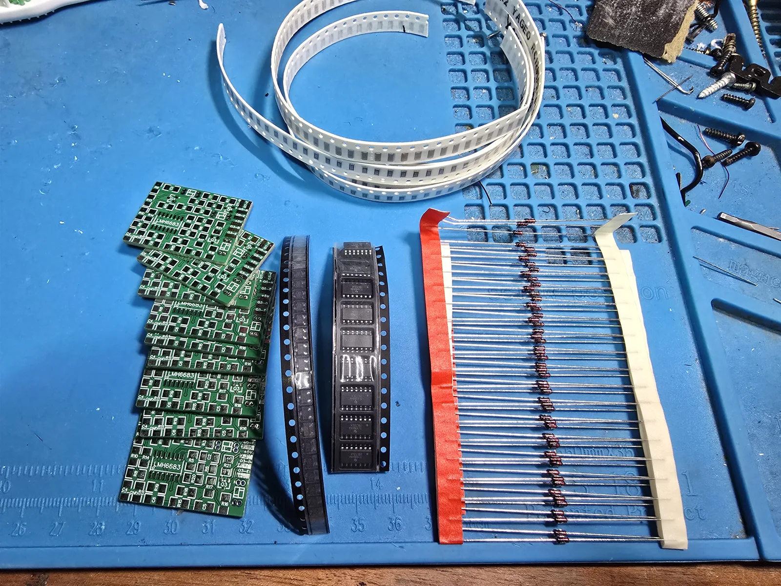
Bill of materials
Everything except the diodes is surface mount. All resistors and capacitors are 1206, which is a forgiving size to hand-solder.
| Part | Value / type | Package | Qty |
|---|---|---|---|
| U1 | TLV3544A (or LMH6683MAX) | SOIC-14 | 1 |
| Q3, Q5, Q7 | 2SA1037AK PNP | SOT-346 | 3 |
| Diodes | 1N4148 (or 1S2076A) | DO-35 | 6 |
| Resistors | 2 kΩ | 1206 | 6 |
| Resistors | 300 Ω | 1206 | 3 |
| Resistors | 200 Ω | 1206 | 6 |
| Resistors | 47 Ω | 1206 | 6 |
| Capacitors | 1 nF | 1206 | 6 |
Plus, for the console side: 5 to 10 10µF ceramic capacitors (0805 is the best fit, 1206 will also fit) and about 2 ft of wire. Anything from 20 to 26 AWG works; I find 22 AWG the easiest to handle.
A note on the silkscreen: the PCB is silkscreened LMH6683 at U1, because that’s the part the original design called for. I fit the TLV3544A instead: it’s a drop-in, and it’s far easier to get. If you’re assembling a bare board and sourcing your own op-amp, either part works in that footprint.
Where each resistor goes
This is the part that isn’t obvious from the board, since the silkscreen carries designators but not values. Every position from R1 to R21 appears exactly once:
| Value | Printed marking | Positions |
|---|---|---|
| 2 kΩ | 2001 | R2, R3, R12, R13, R19, R20 |
| 300 Ω | 3000 | R1, R14, R21 |
| 200 Ω | 2000 | R4, R5, R10, R11, R17, R18 |
| 47 Ω | 47R0 | R6, R7, R8, R9, R15, R16 |
Check the marking, not the bin label. 2001, 2000 and 3000 differ by a
single digit, and 2 kΩ and 200 Ω are easy to mix up if you’re working from an
assortment kit.
All six capacitors are 1 nF: C1 through C6, no per-position distinction. They’re the unmarked tan parts.
Building it, step by step
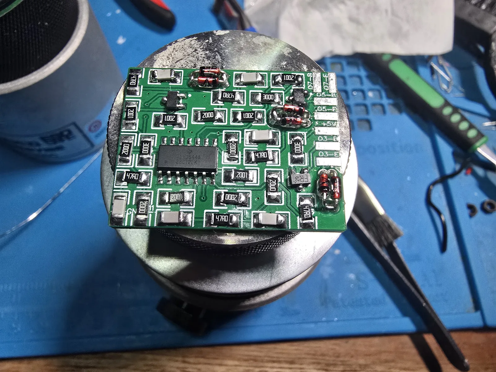
Work lowest-profile first, so nothing you’ve already fitted gets in the way of the iron. Photos below are one board going together on my bench.
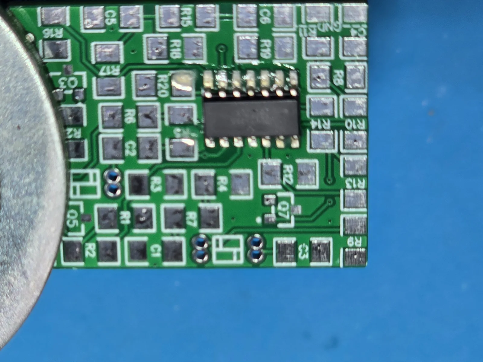
Step 1: U1, the op-amp. Paste the pads, set the package down square, and check it against the silkscreen before you commit. Tack one corner pin first, confirm nothing has shifted, then run the rest.
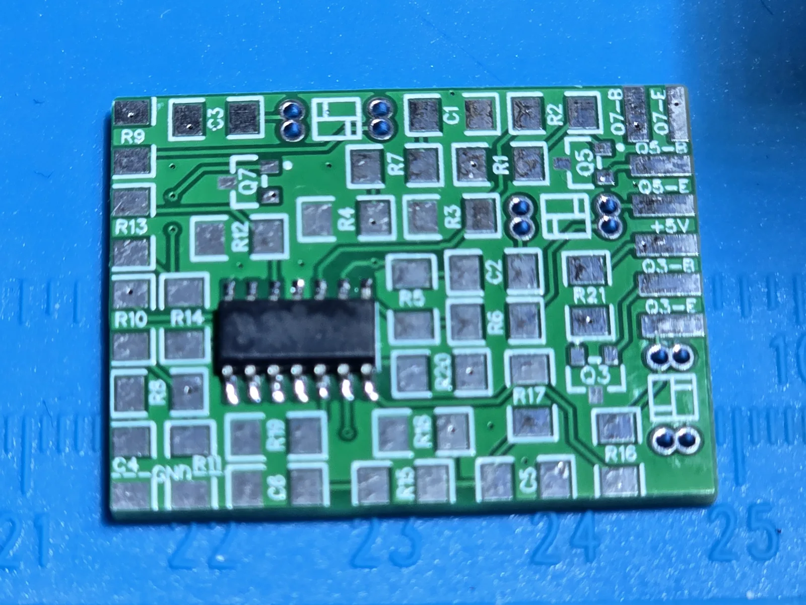
Step 2: the 2 kΩ resistors (R2, R3, R12, R13, R19, R20), marking 2001.
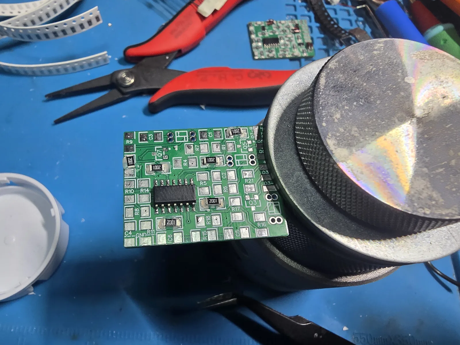
Step 3: the 300 Ω (R1, R14, R21), marking 3000.
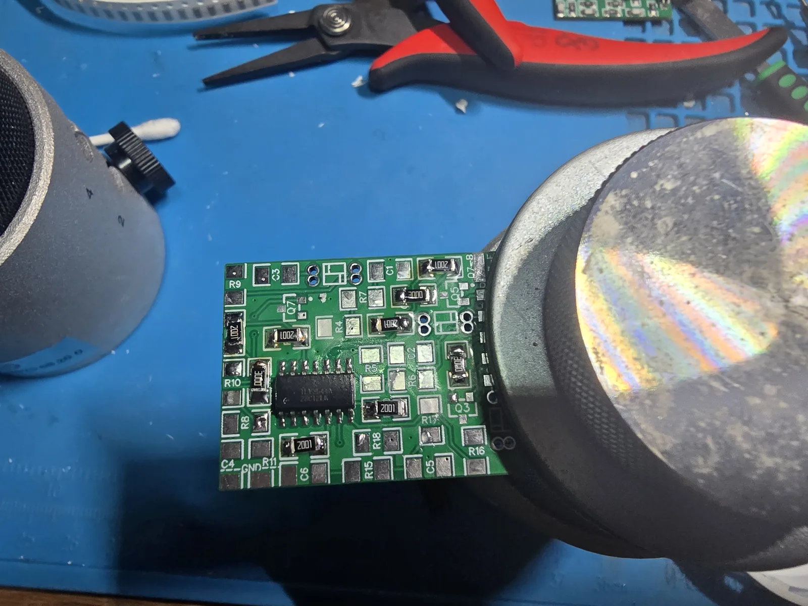
Step 4: the 200 Ω (R4, R5, R10, R11, R17, R18), marking 2000.
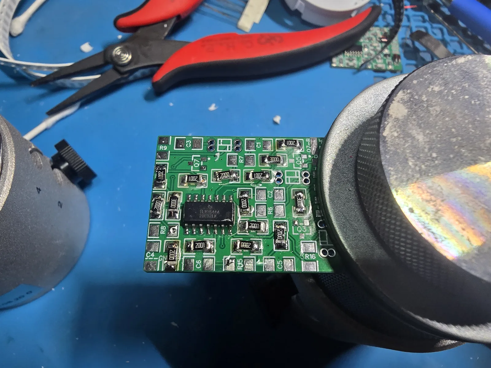
2000 and 2001 end up sitting
next to each other. Worth a second look before you solder.Step 5: the 47 Ω (R6, R7, R8, R9, R15, R16), marking 47R0, and the six
1 nF capacitors at C1–C6.
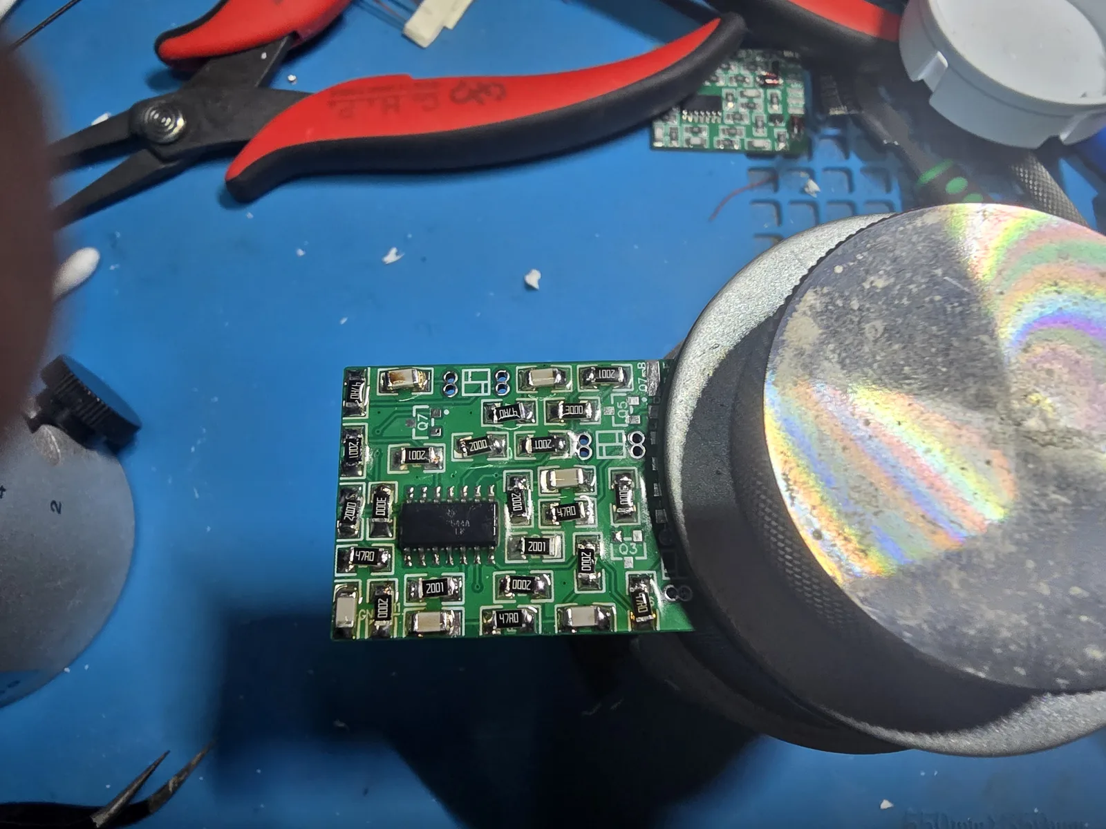
Optional: a pass with hot air. If you have one, going over the board with hot air reflows the passives and lets surface tension pull each part square on its pads. It is cosmetic. A part sitting slightly crooked is not an electrical problem as long as both ends are wetted to their pads, so skip this if you don’t have the tool. This is the moment for it: every surface-mount part is down and nothing through-hole is in the way yet.
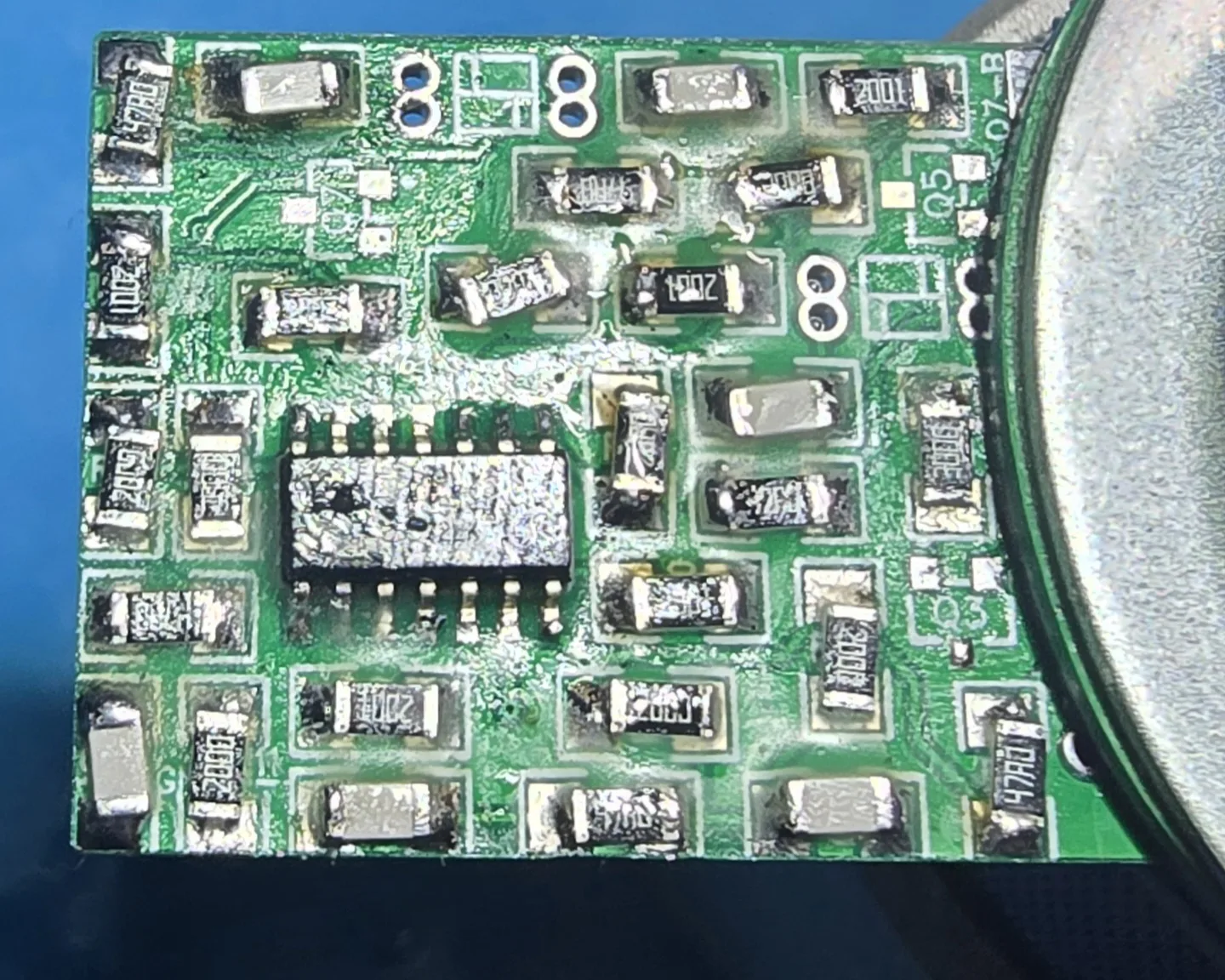
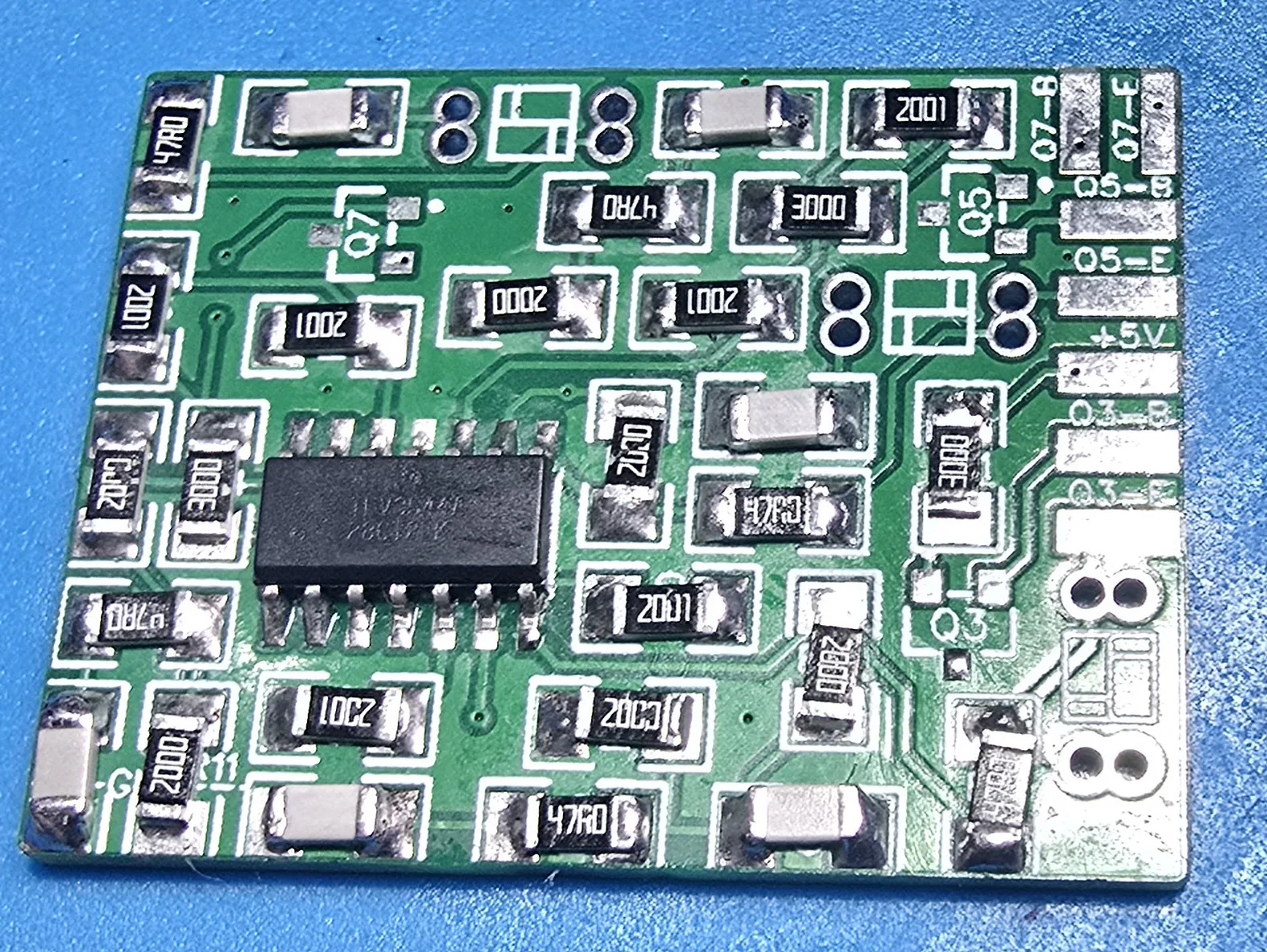
Step 6: the three transistors at Q3, Q5 and Q7. The 2SA1037AK is a 3-leg SOT-346 part. Viewed from above, the way it sits on the board, with the single lone pin pointing up: that lone pin is pin 3, the collector, the left pin is pin 1, the base, and the right pin is pin 2, the emitter.
On SHVC and GPM consoles you can reuse the three transistors you’ll be pulling off the motherboard anyway. On RGB-01/02 boards the originals stay put, so you’ll need three new ones.
Step 7: the six diodes, last, since they’re through-hole and stand tallest.
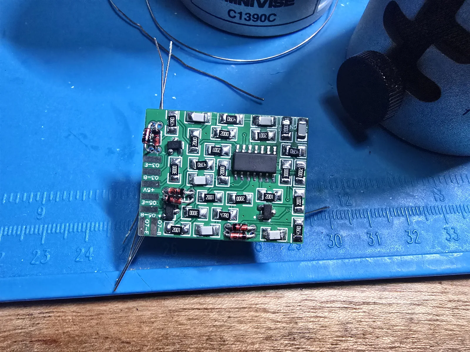
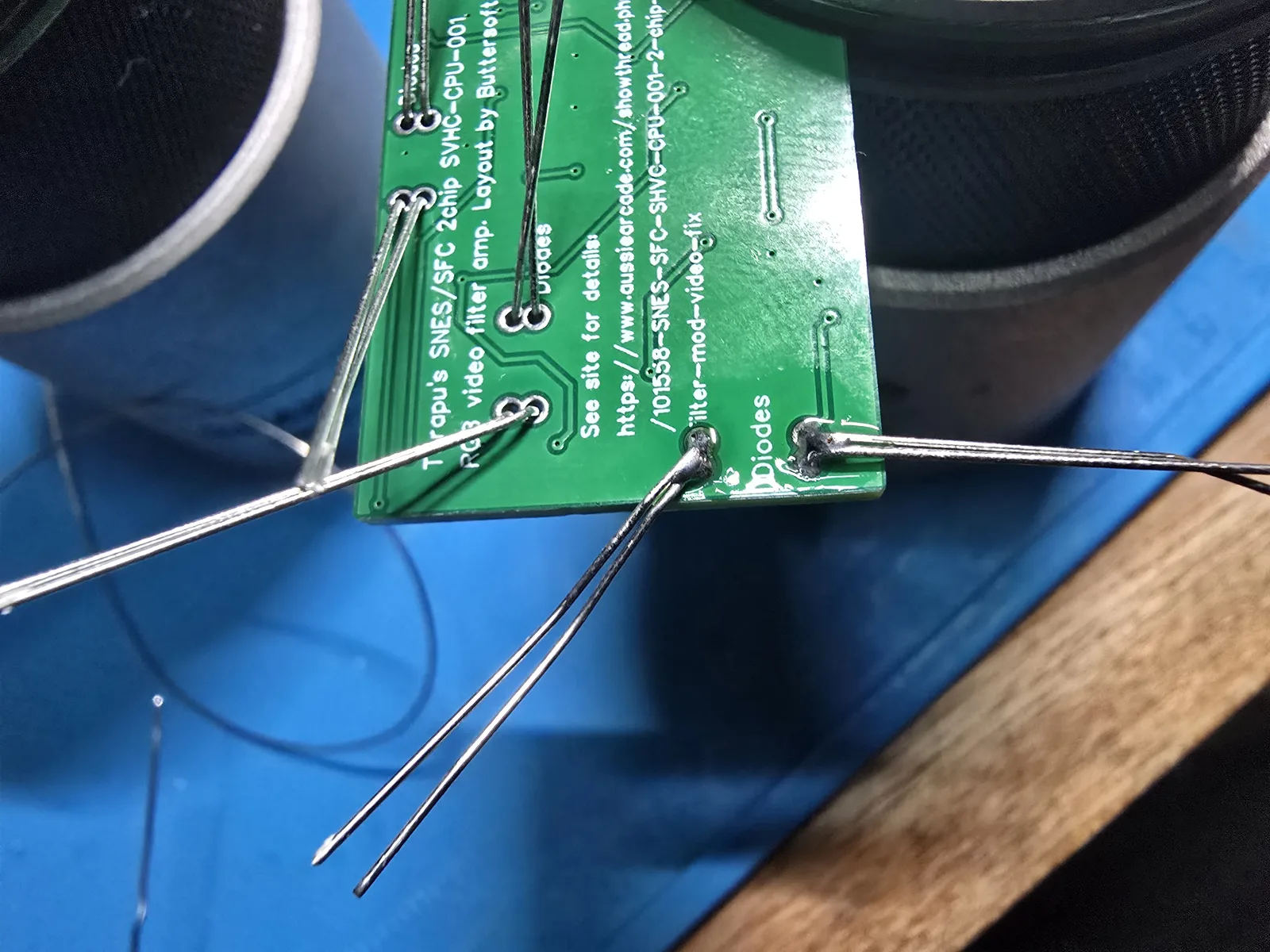
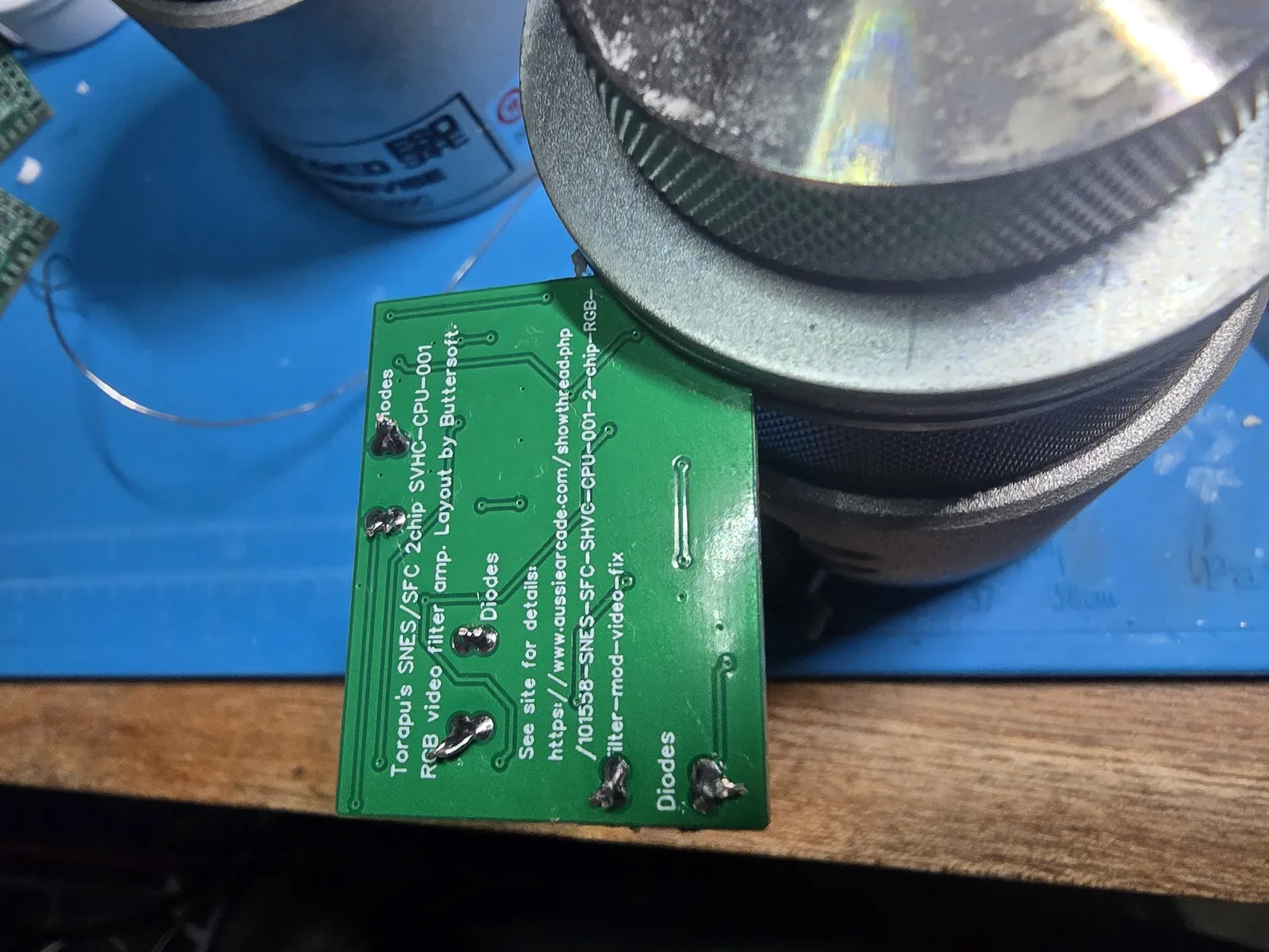
This is the easiest part of the board, not the hardest. Each pair shares both of its nodes, so there is nothing there you can bridge that isn’t already connected. Don’t waste effort keeping the joints separate. The only thing that matters is that the two diodes in a pair point in opposite directions.
Worth knowing what they’re for, because it explains the arrangement. Per Torapu’s original notes, each diode pair in series with its 1 nF cap is the overshoot and undershoot reduction section. Below about 0.6 V the diodes are open and that cap isn’t in the circuit at all, so the sharpening runs at full strength; on a large fast transition the diodes conduct, the cap joins the feedback network, and it damps the ringing that sharpening would otherwise produce. Peaking overshoots on the rising edge and undershoots on the falling one, so the pair is reversed to catch both equally. A single diode would only fix half of it.
Step 8: clean. I clean as I go with IPA, a chem wipe and a brush, and save the ultrasonic for the end, once every part is on the board: Elma tec clean A1 at 2–5% in distilled water at 50–60 °C, followed by a distilled rinse, an IPA displacement and a full dry before any power goes near it.
Bench test before you install it
Test the board on its own before it goes anywhere near a console. It’s much easier to debug on the bench than through eight wires.
1. Tack a pair of wires to the +5V and GND pads so you have something to
clip onto.
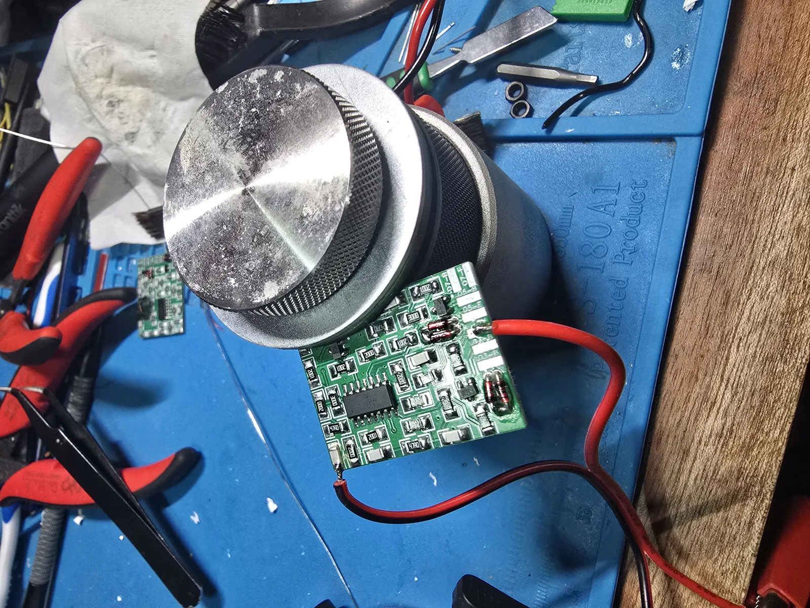
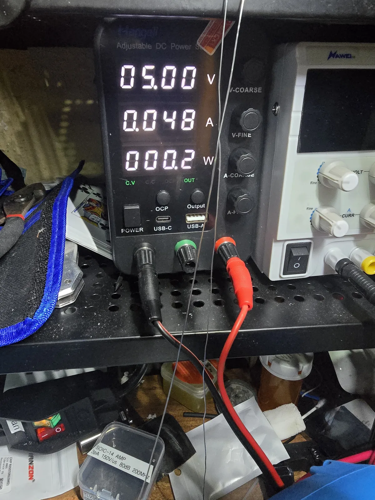
2. Set the bench supply’s current limit before you connect anything. 5.00 V with the limit at ~100 mA. The board draws well under that, so the limit is there to catch a solder bridge before it damages something.
3. Power up and read the current. Expect 48–52 mA quiescent. If it slams into the current limit you have a short; if it reads near zero, the op-amp isn’t getting power.
4. Check each channel: two frequencies, and compare them. Set the generator
to 0.70 Vpp with a DC offset of about +0.5 V, feed an input (say Q3-B), and
watch the matching output (Q3-E) with a second probe. Measure both traces
at each frequency and work in ratios:
| Frequency | Expected output ÷ input |
|---|---|
| 100 kHz | 1.0 (output the same size as input) |
| 5 MHz | ~2.2 (output roughly twice the input) |
Then repeat for green and blue.
Working in ratios is deliberate. Absolute figures depend on what your generator really delivers, on your cables and on your probes, none of which you can trust to a few percent, but the board’s own response at 100 kHz is a perfect reference for its response at 5 MHz. If both ratios land, the board is right regardless of what your rig is doing.
If your generator won’t reach 5 MHz, use 1 MHz and expect a ratio of about 1.33. It’s a weaker test (a wrong peaking component barely shifts 1.33 but moves 2.2 a long way), so prefer 5 MHz when you can.
At 5 MHz, use the short spring ground on your probe rather than the long clip lead, otherwise you’ll be measuring your own rig’s ringing.
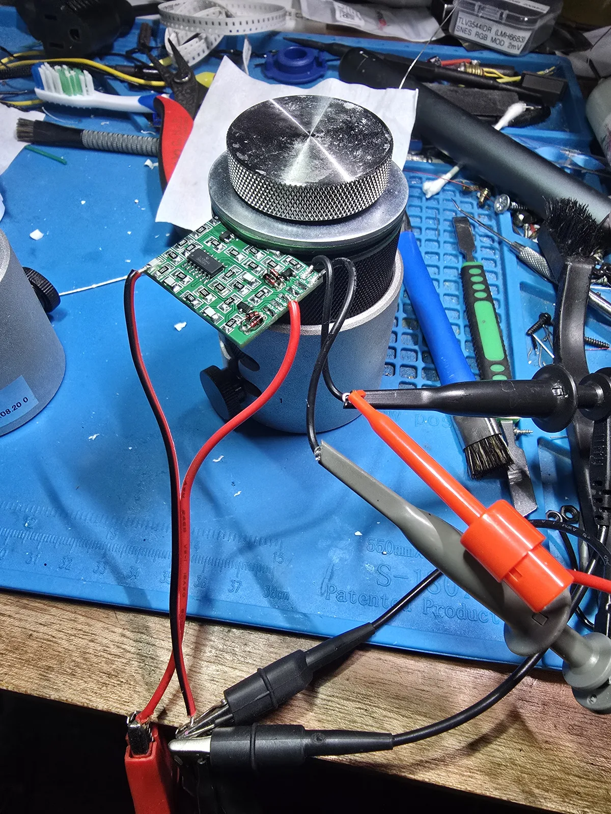
+5V and GND,
probe hooks on the input and output pads of one channel. Tack short wires to the
pads rather than trying to hold a probe tip on them.The offset is not optional. This is a single-supply board (the op-amp runs on +5 V and ground with no negative rail), so a generator centred on 0 V drives the input below ground on every negative half-cycle, outside the op-amp’s usable common-mode range. You’ll get a distorted reading, and it isn’t a condition the circuit ever sees in a console, where the RGB signal rides on a positive DC pedestal. Bias it so the whole swing stays above ground.
Two things that look wrong and aren’t:
- The voltage at the input pad won’t match the generator setting. The signal arrives through a 2 kΩ series into a 2 kΩ to ground, so with the dial at 0.70 Vpp the pad reads more like 900 mV. Don’t compute a gain figure from the dial and expect it to mean anything: this is a sharpener whose gain rises with frequency by design, not a flat amplifier with one gain number.
- The output sits at a higher DC level than the input. There’s a PNP emitter follower ahead of the op-amp, and its emitter rests about one Vbe above its base; the single-supply output also has to rest at a positive operating point. The absolute DC levels on the bench aren’t the in-circuit levels either, since the console feeds this node from its own RGB stage.
Expect the quiescent current to rise a few mA (around 52 to 55 mA) while a channel is being driven, since the output stage is now working into the internal feedback and peaking network.
The real pass criterion is that all three channels match each other, at identical settings. For a circuit whose gain is deliberately frequency-dependent, channel-to-channel consistency tells you far more than any single number does.
Order matters here, and getting it wrong will destroy the op-amp. Power the board first and confirm the quiescent current, then connect and start the generator. On the way out, stop the generator first and cut the supply last. Never leave a signal driving an input on a board that isn’t powered.
The reason is that the op-amp has clamp diodes from each input to the supply rails. With the supply off, V+ sits at 0 V, so any input above about 0.6 V forward-biases the input-to-V+ clamp and injects current straight into the rail. On a CMOS part like the TLV3544 that injection can trigger the parasitic SCR between V+ and ground: the chip latches into a dead short across the rails, and if the supply feeds it, the die fuses and the short becomes permanent. I killed a chip this way: 48 mA one minute, a hard 4.6 Ω between +5V and GND the next, with the thermal camera showing the heat coming from nowhere but the op-amp. The board underneath was fine and a new op-amp brought it straight back to 52 mA.
A tight current limit is your safety net. A latch-up that gets starved will often clear on a power cycle; one that gets fed will not.
Set the generator amplitude by what the scope actually shows, not the front-panel number: generator outputs are usually calibrated into 50 Ω and read about double into a scope’s 1 MΩ input. And land your probe grounds properly: a floating probe ground will happily invent a waveform that isn’t there.
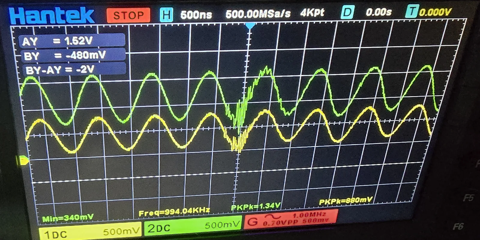
0.70VPP 500mv, that's the DC offset described above. Every
assembled board I sell gets this test on all three channels before it ships.
This is a single un-averaged capture and it caught a burst of external
interference across both traces; with averaging on, both the burst and the
inflated peak-to-peak figures settle down.The measured frequency response
This is a sharpener, so its gain is deliberately not flat. I swept a finished board on the bench with the generator at 0.70 Vpp and +0.5 V offset, measuring input and output at each point, with acquisition averaging on:
| Frequency | Input | Output | Ratio | dB |
|---|---|---|---|---|
| 100 kHz | 680 mV | 680 mV | 1.00 | 0.0 |
| 300 kHz | 680 mV | 720 mV | 1.06 | +0.5 |
| 1 MHz | 690 mV | 920 mV | 1.33 | +2.5 |
| 2 MHz | 700 mV | 1.28 V | 1.83 | +5.2 |
| 3 MHz | 700 mV | 1.46 V | 2.09 | +6.4 |
| 5 MHz | 720 mV | 1.56 V | 2.17 | +6.7 |
| 7 MHz | 780 mV | 1.64 V | 2.10 | +6.5 |
| 10 MHz | 1.0 V | 1.84 V | 1.84 | +5.3 |
| 15 MHz | 1.3 V | 2.1 V | 1.62 | +4.2 |
Unity at baseband, peaking at +6.7 dB at 5 MHz, rolling off above. The SNES pixel clock is 5.37 MHz, so the boost sits right on the frequency where a 2-chip console’s detail lives.
Two things about that curve matter. It is exactly 1.00 at low frequency, so the mod sharpens without altering video levels: brightness and saturation come through untouched. And the peak is a broad plateau from 3 to 7 MHz rather than a narrow spike, which covers the whole detail band instead of ringing at one frequency.
Measured on my own bench with a 150 MHz scope and its built-in generator. Above about 10 MHz the numbers get soft: the generator’s delivered amplitude wanders, and input and output leads on clip leads start coupling to each other. That’s well outside the band this board exists to serve, so I wouldn’t read much into the top two rows.
Installing the board
Step 1: Open up and identify your revision
Disassemble the console and remove the main logic board from the shell. Find the revision in white silkscreen on the board. This guide covers SHVC-CPU-01, SNS-CPU-GPM-01/02 and SNS-CPU-RGB-01/02.
Step 2: Mount the mod board
Read the whole wiring section before you stick anything down. The decoupling caps you’ll want to refresh are easy to cover up with the mod board if you mount it first.
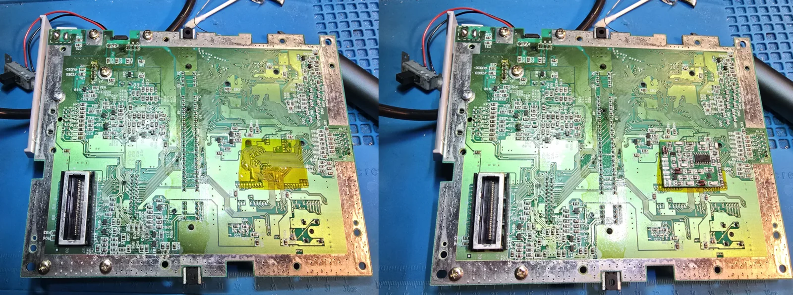
- Find a flat area on the underside of the motherboard. The large empty space next to the cartridge slot is usually the right spot. You want no components underneath the board.
- Clean the area with isopropyl alcohol.
- Lay down Kapton tape where the board will sit. This insulation is not optional.
- Secure the board on top of the tape. Hot glue on the corners works best in my experience; double-sided tape or more Kapton also works.
Step 3: Refresh the video-rail capacitors
Recommended, not required. The video signal is the end of a chain (PPU, VRAM,
encoder), and the original 0.1µF decoupling caps on those rails are decades
old. You can replace them outright or just stack the new 10µF caps on top of the
originals so they sit in parallel. Which positions depends on your revision:
- SHVC-CPU-01, GPM-01, GPM-02:
C83(stock RGB amp section),C92(S-PPU2),C93andC94(the two VRAM chips). - RGB-01, RGB-02:
C53andC64(the RGB chip, this revision’s equivalent of S-ENC),C72(PPU2),C73andC74(the two VRAM chips).
Step 4a: Wiring (SHVC-CPU-01, GPM-01, GPM-02)
These boards keep their RGB amplifier components near the video encoder.
Remove the stock transistors at Q3, Q5 and Q7 from the motherboard, and clean the pads. These are the same 2SA1037AK parts the mod board uses, so if you’re building a bare board you can move them straight over.
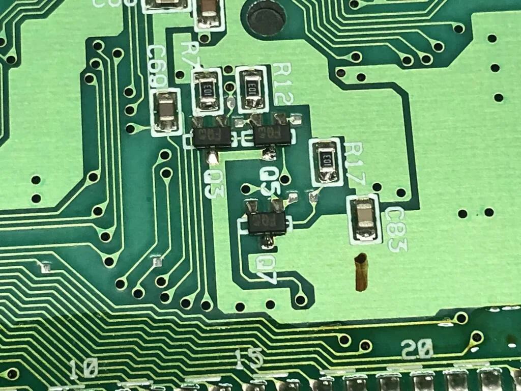
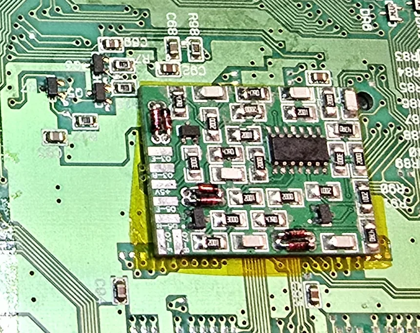
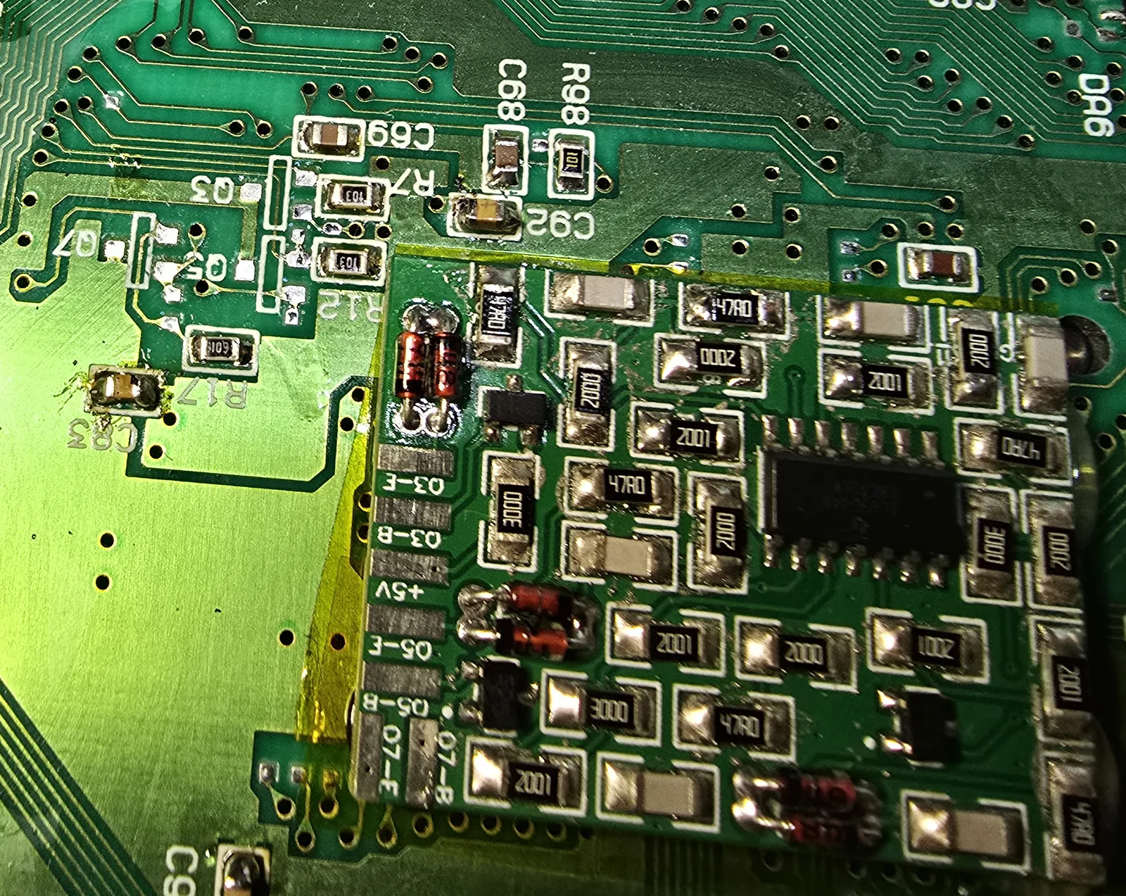
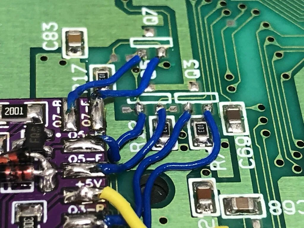
Then run six signal wires. Remember the pinout: with the lone pin pointing up, left is pin 1 (base), right is pin 2 (emitter).
| Signal | From motherboard | To mod board |
|---|---|---|
| Red in | Q3 pad 1 (left) | Q3-B |
| Red out | Q3 pad 2 (right) | Q3-E |
| Green in | Q5 pad 1 (left) | Q5-B |
| Green out | Q5 pad 2 (right) | Q5-E |
| Blue in | Q7 pad 1 (left) | Q7-B |
| Blue out | Q7 pad 2 (right) | Q7-E |
For each of the three output wires there’s an easier alternative to the transistor pad: a nearby 10k resistor labelled 103, sitting very close to the pad. It may be marked R7 (red), R12 (green) or R17 (blue). Confirm with a continuity check before you solder to it.
Step 4b: Wiring (SNS-CPU-RGB-01, SNS-CPU-RGB-02)
These boards use a different amplifier design, near the centre of the board just below the cartridge port on the underside. Here you intercept the signal at the stock transistors instead of removing them.
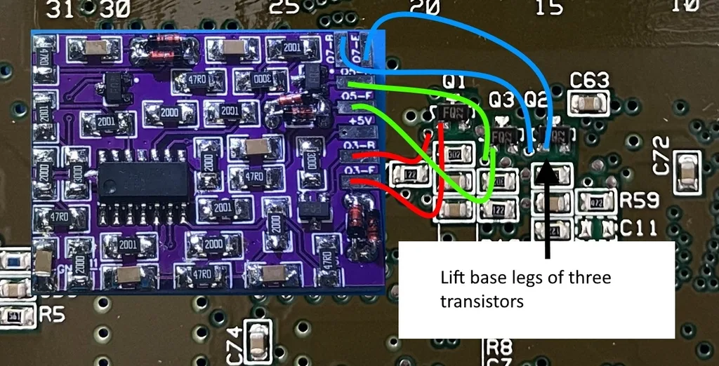
Do not remove anything. Locate the transistors at Q1, Q2 and Q3 on the motherboard and gently lift the base leg (the left pin) of each with tweezers or a dental pick. Slide a small piece of Kapton tape under each lifted leg so it can’t fall back onto its pad.
Then run six wires. The input wires go to the pad the leg came off; the output wires go to the lifted pin itself.
| Signal | From motherboard | To mod board |
|---|---|---|
| Red in | Q1 base pad | Q3-B |
| Red out | Q1 base pin (lifted) | Q3-E |
| Green in | Q3 base pad | Q5-B |
| Green out | Q3 base pin (lifted) | Q5-E |
| Blue in | Q2 base pad | Q7-B |
| Blue out | Q2 base pin (lifted) | Q7-E |
Soldering to the bare pad under a lifted leg is close to impossible. Use the via immediately next to it instead, and confirm with a continuity check that you’ve got the right one. When you solder the output wires, make sure the Kapton is still in place so you don’t accidentally bridge the pin back to the pad you just lifted it off.
Step 5: Power
Two more wires, for eight total.
- +5V: the regulator output is my preference; the positive pad of C83 also works. Do not take it from the positive leg of the biggest capacitor on the board. That’s unregulated input voltage, not the 5V rail, and it will destroy the board.
- GND: the reset switch is nearby and two of its pads are ground, which is where I usually go. The negative pad of C83 works too. Make only one ground connection.
Step 6: Test before you button it up
Set the motherboard loosely back in the bottom half of the shell, connect power and an RGB SCART cable, insert a game and power on. You should get a clear, sharp picture.
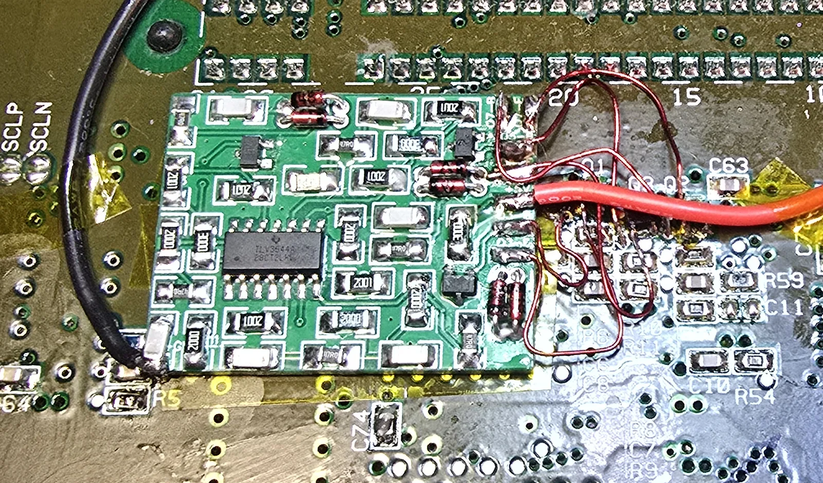
Once it’s confirmed working, tack the wires down with a little hot glue, tape or solder mask so they can’t vibrate loose later.
Optional extras
PPU pin lift, for jailbars
The console’s composite video circuitry injects noise into the RGB signal, and it’s a common source of faint vertical or diagonal lines. Lifting one pin on S-PPU2 disables that circuitry.
Apply gentle upward pressure on the pin with a dental pick or fine tweezers, briefly touch it with the iron to reflow the joint, and lift it clear of the pad. Bend it straight up so it can’t touch anything.
- SHVC-CPU-01, GPM-01, GPM-02: lift pin 27 (5MOUT, the 5 MHz signal used for composite and RF).
- RGB-01, RGB-02: lift pin 3 (3.58M, the 3.58 MHz signal used for composite and RF).
This disables composite and RF output. If you want those, skip it.
Full recap
While the console is apart it’s a good time to replace all the electrolytics. Console5 and others sell revision-specific cap kits.
Skip the 270pF capacitors
Older community guides mention adding 270pF caps between base and collector of Q4, Q6 and Q8. Buttersoft walked that back in his own thread, and testing since has agreed: they aren’t necessary with this board and can make the image worse. Leave them off.
Troubleshooting
Black screen, but game audio is present. The board probably isn’t getting
power, or the power wires are reversed. Check +5V and GND: secure, not
bridged, and on the right points.
“No signal”, completely black, no audio. This mod doesn’t touch the sync signal, so no signal at all usually means something unrelated to the mod. Re-check the multi-out wiring, try a known-good SCART cable, and confirm your TV or scaler works with another console.
Wrong colours, or one colour missing. A wiring problem on the RGB lines. Re-check all six in/out connections for bridges and swaps. On RGB-01/02 boards, check you haven’t mixed up the transistor legs.
Still blurry, or heavy ghosting. The old amplifier isn’t fully out of circuit. On SHVC/GPM, confirm Q3, Q5 and Q7 were completely removed. On RGB-01/02, confirm all three base legs are properly lifted and insulated from their pads.
If you suspect the board itself, pull it and run the bench test.
Schematic
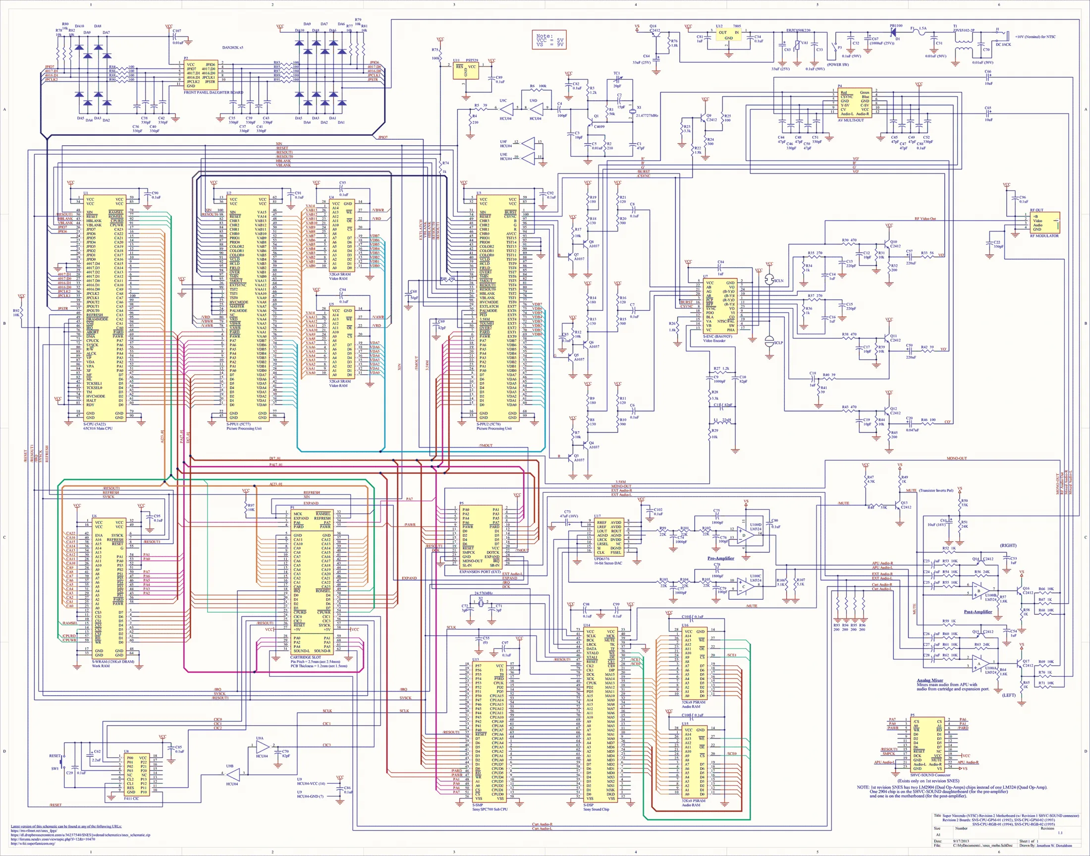
This multi-revision schematic by Jonathon W. Donaldson covers the SHVC, GPM and RGB variants together, so some labels won’t match your particular board exactly.
Support
All support is best effort. I’m happy to answer questions, look at pictures and help you troubleshoot. I’m not ultimately responsible for making the mod work for you, or for fixing problems created while installing it. Message me any time.
Credit and resources
This mod is open source. The circuit is Torapu’s design and the PCB layout is Buttersoft’s. I print the boards, source the parts, and hand-assemble and test every unit. This guide also owes a lot to Antonio Maiorano, Jonathon W. Donaldson, and the contributors to Console5 and superfamicom.org.
- This page is the authoritative copy of the guide. An older version lived in my GitLab repository and now just points here. If you want an offline copy, print this page: it has a print stylesheet and will lay out properly on paper.
- SNES / SFC SHVC-CPU-001 2-chip RGB filter mod video fix, Buttersoft’s original post, via the Internet Archive
- SNES Edge Enhancement Mod by Torapu/Buttersoft, install and CRT footage
- SNES 2-Chip RGB Filter Mod, Antonio Maiorano’s write-up
- SNES 2-Chip RGB Filter Mod: SNS-CPU-RGB-02, his RGB-02 guide
- SNES Schematics, Ports, and Pinouts
- SNES Tech Wiki, including capacitor lists
← Back to the SNES RGB Mod Board (Buttersoft/Torapu Design) for 2-Chip Super Nintendo listing